EP0622840A2 - Apparat und Methode für die Montage und das Prüfen von Monolitisch integrierten Mikrowellenschaltungsmodulen (MMIC) - Google Patents
Apparat und Methode für die Montage und das Prüfen von Monolitisch integrierten Mikrowellenschaltungsmodulen (MMIC) Download PDFInfo
- Publication number
- EP0622840A2 EP0622840A2 EP94105397A EP94105397A EP0622840A2 EP 0622840 A2 EP0622840 A2 EP 0622840A2 EP 94105397 A EP94105397 A EP 94105397A EP 94105397 A EP94105397 A EP 94105397A EP 0622840 A2 EP0622840 A2 EP 0622840A2
- Authority
- EP
- European Patent Office
- Prior art keywords
- active elements
- combination
- characteristic value
- substrate
- results
- Prior art date
- Legal status (The legal status is an assumption and is not a legal conclusion. Google has not performed a legal analysis and makes no representation as to the accuracy of the status listed.)
- Granted
Links
Images


Classifications
-
- H—ELECTRICITY
- H10—SEMICONDUCTOR DEVICES; ELECTRIC SOLID-STATE DEVICES NOT OTHERWISE PROVIDED FOR
- H10P—GENERIC PROCESSES OR APPARATUS FOR THE MANUFACTURE OR TREATMENT OF DEVICES COVERED BY CLASS H10
- H10P72/00—Handling or holding of wafers, substrates or devices during manufacture or treatment thereof
- H10P72/06—Apparatus for monitoring, sorting, marking, testing or measuring
- H10P72/0612—Production flow monitoring, e.g. for increasing throughput
-
- H—ELECTRICITY
- H10—SEMICONDUCTOR DEVICES; ELECTRIC SOLID-STATE DEVICES NOT OTHERWISE PROVIDED FOR
- H10P—GENERIC PROCESSES OR APPARATUS FOR THE MANUFACTURE OR TREATMENT OF DEVICES COVERED BY CLASS H10
- H10P74/00—Testing or measuring during manufacture or treatment of wafers, substrates or devices
- H10P74/23—Testing or measuring during manufacture or treatment of wafers, substrates or devices characterised by multiple measurements, corrections, marking or sorting processes
-
- H—ELECTRICITY
- H10—SEMICONDUCTOR DEVICES; ELECTRIC SOLID-STATE DEVICES NOT OTHERWISE PROVIDED FOR
- H10W—GENERIC PACKAGES, INTERCONNECTIONS, CONNECTORS OR OTHER CONSTRUCTIONAL DETAILS OF DEVICES COVERED BY CLASS H10
- H10W90/00—Package configurations
- H10W90/701—Package configurations characterised by the relative positions of pads or connectors relative to package parts
- H10W90/751—Package configurations characterised by the relative positions of pads or connectors relative to package parts of bond wires
- H10W90/754—Package configurations characterised by the relative positions of pads or connectors relative to package parts of bond wires between a chip and a stacked insulating package substrate, interposer or RDL
Definitions
- This invention relates to an apparatus and a method for manufacturing a microwave circuit module, and more particularly to a method of assembling and checking microwave circuit modules which are used for microwave communication systems and the like.
- An MMIC microwave monolithic integrated circuit
- An ultra-high frequency integrated circuit is greatly different from the general digital IC in that it cannot be realized only with lumped parameter circuits but requires distributed constant circuits.
- the above integrated circuit is not suited for integrating therein distributed constant circuits in a large scale.
- the distributed constant circuit has a size determined by the wavelength, and it usually requires a great space for installation or mounting.
- the increased size in the MMIC is disadvantageous from the points that gallium arsenide (GaAs) is often utilized, that thin wafers are preferred in view of characteristic requirements, and that the price becomes high.
- GaAs gallium arsenide
- the MMIC is not suited for the large-scale integration.
- Fig. 10 shows the composite microwave circuit module disclosed in the patent application referred to above.
- a dielectric substrate which is formed as a lamination of multiple layers is provided with ground surfaces formed of conductive layers comprised of an upper and a lower layer 26 and 23, and signal circuits 24 and 25 formed of one or more conductive layers for signal transmission and disposed in an intermediate layer portion of the substrates.
- a shield surrounding the signal circuits 24 and 25 is formed by thorough-holes 32 and 34 which are formed around the signal circuits 24 and 25 for short-circuiting the two ground surfaces.
- These circuits include active elements 28, such as MMICs, ICs, transistors, diodes, etc., and passive elements, which are formed by patterning of strip lines, microstrip lines, coplanar lines, etc, these elements being electrically connected to one another to obtain an integrated structure.
- a base plate at 21 a layered capacitor, at 22 a conductive cap, at 27 a wiring or interconnect layer, at 29 a signal line pattern, at 30 a power source pattern, at 31 a bonding wire, at 33 a chip installation land, at 35 a conductor pattern, and at 36 a land.
- the active elements and the divided connection substrate for interconnecting these elements are realized by use of interconnect patterns within the integrated multi-layer substrate, whereby the characteristic deterioration caused by connection is precluded and the number of process steps in the fabrication is reduced.
- the interference due to coupling of the microwave circuits that results from the accommodation of the circuits in a common case and the resonance that results from the case as a cavity are avoided by the provision of a shield structure or a cavity structure accommodating active elements.
- a dielectric portion above the intermediate layer portion used for signal transmission is removed thereby forming a cavity as a place to install such semiconductor elements as MMICs.
- the semiconductor elements are installed thereat and the ground surface removed at the top is covered with a conductive cap.
- the above seal structure of the composite microwave circuit module realizes an air-tight seal with the conductive cap and provides a protective structure with the conductive cap, whereby the semiconductor elements installed are protected from contamination by external fields.
- the above composite microwave circuit module has the following other features.
- the composite microwave circuit module is with a structure, in which a conductor land (an element installation surface) is provided in the intermediate layer portion and connected to a lower layer ground surface via a plurality of via-holes (for the reduction of RF impedance), and the via-holes are filled with a metal to reduce thermal resistance with respect to the lower layer and to obtain effective heat conduction.
- a conductor land an element installation surface
- the via-holes are filled with a metal to reduce thermal resistance with respect to the lower layer and to obtain effective heat conduction.
- the composite microwave circuit module is with a structure, in which the via-holes are provided right underneath a local heat generation spot such as a transistor region in a semiconductor chip for thermal resistance reduction.
- the composite microwave circuit module is with a structure, in which a plurality of conductor layer lands are provided as alternate capacitor and ground lands between an element-installation surface of the intermediate layer portion and a lower ground layer, with the capacitor lands connected together and the ground surface and the ground lands connected together via via-holes, thus forming a laminate capacitor which functions as a bypass capacitor for an installed element (mounted chip), while dissipating heat laterally through the laminated conductor layer lands to reduce the thermal resistance.
- the composite microwave circuit module is with a structure, in which the intermediate layer portion is provided with a very thin dielectric layer which forms, together with the conductor patterns on both sides of such dielectric layer, capacitive coupling, thus forming a transmission line to cut direct current (DC) component.
- DC direct current
- the composite microwave circuit is with a structure, in which a dielectric layer is formed on an upper ground layer with conductor patterns formed thereon as wiring patterns to obtain power supply wirings.
- the composite microwave circuit module is with a structure, in which, at a portion connected to inner layers, a land is provided to form together with the immediate vicinity ground layer a capacitor as a bypass capacitor to prevent RF leakage from the inner layers.
- the above composite microwave circuit module is manufactured with a technique which permits realizing a large-scale microwave circuit in a compact form.
- it includes a plurality of active elements and these active elements are subject to characteristic fluctuations in manufacture. Therefore, an improvement is called for in this area in order to enhance the yield of the overall manufacturing of the composite microwave modules.
- each element should be given a yield of 98% or above. If the yield is also distributed to the assembling process, the yield for each element is even higher.
- a generally conceivable method to this end is to check electrical characteristics of the composite microwave circuit module after the installation of the active elements and adjust microstrip lines around the active elements according to the check results, thereby obtaining a desired performance.
- This method has a problem in that it is difficult to carry out the adjustment after completion of the assemblage of the module constituting a large-scale circuit.
- Another problem is that the active elements are apt to be contaminated so that, since they cannot be given any seal before completion of the adjustments, the reliability thereof is lowered.
- microstrip lines around the active elements requires a high skill and a long time, thus leading to a high price.
- an apparatus for manufacturing a microwave circuit module having a plurality of active elements mounted on a substrate comprising: a memory means which stores results of checks of characteristics of the active elements immediately after the manufacture with the results being stored individually in correspondence to the active elements; a combination determining means which determines a combination among the active elements such that a characteristic value to be derived from the combination among the active elements based on the results in the memory means is in a predetermined range; a calculating means which calculates a combined predicted characteristic value of the combination based on the results in the memory means on each of those active elements which are determined by the combination determining means; a computing means which, when the combined predicted characteristic value obtained at the calculating means is outside the predetermined range, computes a content and an amount of adjustment to be made in the substrate for the combined predicted characteristic value to be in the predetermined range; a substrate processing means which processes the substrate based on results of computation in the computing means; and an assembling means which assembles the active elements in the combination determined by
- a low cost and highly reliability microwave circuit module at a high overall yield, which is accomplished by storing the results of checks of the respective active elements after the manufacture in correspondence to the individual active elements, determining a combination of active elements according to the stored results or data, calculating the characteristic value of the determined combination according to the results of checks of the active elements in the combination, computing, if the calculated characteristic value is out of a predetermined tolerable range, a content and an amount of adjustment to be made in the combined characteristic value for such value to be in the predetermined tolerable range, and adjusting the substrate according to the result of computation.
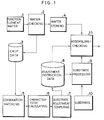
- a wafer checking unit 2 checks all the active elements on a function element wafer 1 and makes selection in them. The results are stored in a function element wafer storage unit 4. Also, the checked results (i.e., characteristic data of the checked active elements) are stored in a chip data unit 3.
- a chip combination matching unit 5 determines an optimum combination of a plurality of active elements according to the data in the chip data unit 3 such that a desired characteristic can be approached by a combination of a plurality of selected and identified active elements.
- a characteristic calculating unit 6 calculates an predicted characteristic, which is obtainable when the plurality of active elements in the combination determined by the chip combination matching unit 5 are assembled as a microwave circuit module.
- a substrate adjustment amount computing unit 7 calculates the amount of adjustment of the microwave circuit module substrate, if it is determined that the characteristic calculated in the characteristic calculating unit 6 is outside a desired standard range. More specifically, the unit 7 determines through simulation a process which is to be added to an adjustable portion prepared in a particular portion of the microwave circuit module substrate in order to obtain a module characteristic that is in the desired standard range. The result of simulation is stored as adjustment process instruction data in an adjustment process instruction data unit 8.
- a substrate adjustment processing unit 9 executes an adjustment processing, as analog circuit tuning with respect to the substrate 10, according to the data stored in the adjustment processing instruction data unit 8, and feeds the adjusted substrate to an assembling/checking unit 11.
- the assembling/checking unit 11 assembles a microwave circuit module by installing the plurality of active elements in the combination, which has been determined by the chip combination matching unit 5, on the substrate having been adjusted in the substrate adjustment processing unit 9. The unit 11 also checks the assembled microwave circuit module and carries out any adjustment that may be found necessary, thus completing the assembling of the microwave circuit module.
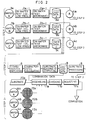
- Fig. 2 is a block diagram illustrating a microwave circuit module assembling operation in an embodiment of the invention. The microwave circuit module assembling operation in the embodiment of the invention will be described with reference to Figs. 1 and 2.
- Active elements A, B and C respectively on function element wafers 1a, 1b and 1c are all checked in on-wafer tests 2a-1, 2b-1, and 2c-1 which are conducted in the wafer checking unit 2.
- the on-wafer tests 2a-1 to 2c-1 are carried out under DC or low frequency range, and checks as to any wiring pattern defect and makes evaluation under low frequency for each of a large number of circuit chips which are provided on a single wafer.
- completely defective circuit chips are also discriminated according to the data obtained by the defect checks and the low frequency evaluation of the wiring patterns noted above.
- the active elements A to C on the function element wafers 1a to 1c are all checked in on-wafer tests 2a-2, 2b-2 and 2c-2 in the wafer checking unit 2.
- characteristic check i.e., function check, is done by using a high frequency probe at an actually used high frequency.
- the above function check data are stored together with the test results in the on-wafer tests 2a-1 to 2c-1 in corresponding chip data units 3a to 3c and, according to these function check data, the circuit chips with the characteristic thereof exceeding a permissible or tolerable fluctuation range are discriminated.
- the chip data units 3a, 3b and 3c store data of circuit chips other than those which are completely defective or the characteristic of which is beyond the permissible fluctuation range.
- the function element wafers 1a to 1c after the checks in on-wafer tests 2a-1 to 2c-1 and 2a-2 to 2c-2 are stored in the function element wafer storage unit 4.
- the function element wafers 4a to 4c are stored in the function element wafer storage unit 4 such that they can be discriminated later.
- the above operation is a processing operation to check all the active elements A to C in the on-wafer tests 2a-1 to 2c-1 and 2a-2 to 2c-2 in step 1 shown in Fig. 2.
- on-wafer test data of the active elements A to C on the function element wafers 1a to 1c, obtained in the step 1, are processed.
- the on-wafer test data are obtained for each of the active elements A to C and also for each of the circuit chips in each wafer, and there are fluctuations among the circuit chips and among the lots.
- the chip combination matching unit 5 finds and matches the optimum combination of such plurality of circuit chips.
- a strategy here is to attach the primary importance to the ability of using as many circuit chips as possible without discarding them. Specifically, a strategy is adopted such as to save as many circuit chips as possible even if there are fluctuations from a desired characteristic within the permissible range rather than selecting a few best combinations with the characteristics thereof centered on the desired characteristic.
- the chip combination matching unit 5 determines the optimum combination of a plurality of active elements according to the data in the chip data section 3 so that a desired characteristic or a characteristic closer thereto is obtained as a result of the combining of a plurality of selected and discriminated active elements.
- a characteristic calculating unit 6 calculates a predicted characteristic that is obtainable when a plurality of active elements A to C in the combination selected in the chip combination matching unit 5 are combined as a microwave circuit module, and checks if the result of calculation is in the desired standard range.
- a substrate adjustment amount computing unit 7 determines through simulation a processing to be applied to a predetermined adjustable portion in the microwave circuit module to obtain a characteristic in the desired standard range.
- the results calculated are stored in an adjustment processing instruction data unit 8 as an adjustment processing instruction data.
- the unit 7 calculates the above adjustment processing instruction data for every set of the plurality of active elements A to C in the combination selected in the chip combination matching unit 5.
- a substrate adjustment processing unit 9 adjusts the substrate according to the data for each set of the plurality of active elements A to C that are stored in the adjustment processing instruction data unit 8.
- the adjustment is done by a method based on wire bonding, a method of cutting or removing a strip line pattern portion through evaporation thereof caused by exposure to a laser beam, or a method of bonding a ferroelectric piece.
- step 3 shown in Fig. 2 the set of active elements A to C in the selected combination and corresponding substrate 10a after the adjustment processing, are assembled together, and the system thus obtained is checked. It is suitable to use a specially prepared robot for this step 3.
- a machine For obtaining a correct circuit chip combination, a machine can make a more accurate handling than a man can.
- the assembling equipment suited for picking up and assembling circuit chips in a combination selected from a plurality of stored function element wafers 4a to 4c, it is suitable to use a robot as dedicated equipment.
- step 3 divisions 12a to 12c of the respective function element wafers 4a to 4c into circuit chip units are made to permit the circuit chips to be picked up.
- step 11a executed in the assembling/checking unit 11, circuit chips of the active elements A to C to be assembled with the substrate 10a after the adjustment processing are picked up.
- the substrate 10a after the adjustment processing and the picked-up circuit chips are bonded together by die bonding, the wire bonding is added, and then a cover is mounted to seal a circuit chip accommodation section.
- a checking step 11b is executed, in which a check is done as to whether the characteristic of the assembled microwave circuit module is in the standard range.
- Modules with standard characteristic are good products but, for those in which the characteristic thereof is not in the standard range, a next adjustment step 11c may be provided. To carry out such adjustment on a large scale, however, may lead to possible demerits and, therefore, the adjustment in the adjusting step 11c is limited to a small scale.
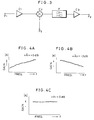
- Fig. 3 and Figs. 4A to 4C are diagrams for explaining the determination of the combination in the chip combination matching unit 1 shown in Fig. 1. The determination of combination in the chip combination matching unit 5 will now be described with reference to Fig. 3 and Figs. 4A to 4C.
- the algorithm underlying the matching in the chip combination matching unit 5 varies with the functions of the intended microwave circuit module.
- a frequency converter/amplifier module as shown in Fig. 3 is taken up for explanation.
- designated at C1 is an RF amplifier chip, at C2 a mixer chip, at C3 an IF amplifier chip, at F a filter, at P1 an RF terminal, at P2 an LO terminal, and at P3 an IF terminal.
- the transfer function from the RF terminal P1 to the LO terminal P2 is basically the product of multiplication of the characteristics of the RF amplifier chip C1, the mixer chip C2, the filter F and the IF amplifier chip C3.
- the RF and IF amplifier chips C1 and C3 in this circuit fluctuate in two respects, i.e., the gain-frequency characteristic and average gain, a method used is not to take only the best characteristic matching from the combinations of a large number of circuit chips, but to take as many circuit chips as possible as usable ones by saying those which may otherwise be discarded. The method for doing so will now be described.
- the overall gain-frequency characteristic of the combination approaches a flat characteristic (see Fig. 4C).
- the average gain can be brought close to a desired total gain.
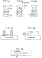
- Figs. 5A to 5C are diagrams showing an example of the result of calculation in the substrate adjustment amount computing unit 7 shown in Fig. 1.
- Fig. 5A shows the state before the adjustment
- Fig. 5B shows the state in which the resistance is increased by the cutting of a resistor pattern 50 between electrode patterns 52 and 53 with a laser beam 55
- Fig, 5C shows the state in which the resistance is reduced by wire bonding 57.
- adjustment in a predetermined range is possible if an amplitude equalizer is assembled in the substrate.
- the adjustment may be made by changing one or more internal resistance values.
- the resistance value or values are varied by a method shown in Fig. 5B or 5C.
- Figs. 6A to 6C are diagrams showing the substrate adjustment processing executed in the substrate adjustment processing unit 9 shown in Fig. 1.
- Fig. 6A shows a method of adjustment by wire bonding 62
- Fig. 6B shows a method of adjustment by cutting or removing a microstrip line portion by evaporation caused by exposure to a laser beam 64
- Fig. 6C shows a method of adjustment by bonding a ferroelectric piece 66.
- Fig. 7 shows the operation of assembling a microwave circuit module in a different embodiment of the invention.
- the embodiment shown therein has the same structure as that of the preceding embodiment of the invention except that a substrate characteristic checking step 13 is provided in the step 2 shown in Fig. 2.
- a substrate characteristic checking step 13 is provided in the step 2 shown in Fig. 2.
- Like elements are thus designated by like reference numerals and symbols. Like elements operate in the same way as in the preceding embodiment of the invention.
- the characteristic of the substrate, on which the circuit chips in the combination determined by the chip combination matching unit 5 are to be mounted is measured in the substrate characteristic checking step 13, and measurement data thus obtained is supplied to the characteristic calculating unit 6.
- the characteristic calculating unit 6 calculates the predicted characteristic, which is expected from combining, as microwave circuit module, these circuit chips and the substrate. The unit 6 then checks whether the result of calculation is in a desired standard range.
- the substrate adjustment amount computing unit 7 determines, through simulation, a processing to be applied to a predetermined adjustable in the microwave circuit module substrate for obtaining a characteristic in a desired standard range.
- the result of the simulation is stored as adjustment processing instruction data in the adjustment processing instruction data unit 8.
- the substrate adjustment amount computing unit 7 calculates the adjustment processing instruction data for each set of a plurality of active elements A to C in the combination selected in the chip combination matching circuit 5 and a substrate corresponding thereto.
- the substrate adjustment processing unit 9 adjusts the substrate, the characteristic of which has been measured in the substrate characteristic checking step 13, according to the data of the set of the plurality of active elements A to C stored in the adjustment processing instruction data unit 8 and the corresponding substrate data. In this way, adjustment of the substrate can be done in correspondence to the substrate fluctuations in manufacture.
- Fig. 8 is a block diagram showing a different embodiment of the structure according to the invention.
- This embodiment has the same structure as that of the previous embodiment of the invention shown in Fig. 1 except that in this embodiment a deviation analysis statistical processing unit 14 is provided, which statistically processes the result of checking in the assembling/checking unit 11 and feeds back the result of the processing to the chip combination matching unit 5.
- a deviation analysis statistical processing unit 14 is provided, which statistically processes the result of checking in the assembling/checking unit 11 and feeds back the result of the processing to the chip combination matching unit 5.
- Like elements are designated by like reference numerals and symbols. Also, like elements operate in the same way as in the previous embodiment of the invention.
- the deviation analysis statistical processing unit 14 statistically processes the characteristic of the microwave circuit module as obtained in the assembling/checking unit 11 for analyzing a deviation with respect to the predicted value.
- the unit 14 Feeds back the result of processing to the processing in the chip combination matching unit 5 and following units.
- the processing in the chip combination matching unit 5 and following units may be carried out in such a manner as to compensate for the above deviation. For example, if the calculated compensation amount is excessive, the amount of processing on the substrate may be reduced.
Landscapes
- Microwave Amplifiers (AREA)
- Semiconductor Integrated Circuits (AREA)
- Testing Or Measuring Of Semiconductors Or The Like (AREA)
Applications Claiming Priority (3)
| Application Number | Priority Date | Filing Date | Title |
|---|---|---|---|
| JP105014/93 | 1993-04-07 | ||
| JP5105014A JPH0821807B2 (ja) | 1993-04-07 | 1993-04-07 | マイクロ波回路モジュールの製造装置 |
| JP10501493 | 1993-04-07 |
Publications (3)
| Publication Number | Publication Date |
|---|---|
| EP0622840A2 true EP0622840A2 (de) | 1994-11-02 |
| EP0622840A3 EP0622840A3 (de) | 1995-03-22 |
| EP0622840B1 EP0622840B1 (de) | 2000-09-06 |
Family
ID=14396218
Family Applications (1)
| Application Number | Title | Priority Date | Filing Date |
|---|---|---|---|
| EP94105397A Expired - Lifetime EP0622840B1 (de) | 1993-04-07 | 1994-04-07 | Methode für die Montage und das Prüfen von monolitisch integrierten Mikrowellenschaltungsmodulen (MMIC) |
Country Status (7)
| Country | Link |
|---|---|
| US (1) | US5396433A (de) |
| EP (1) | EP0622840B1 (de) |
| JP (1) | JPH0821807B2 (de) |
| AU (1) | AU667769B2 (de) |
| CA (1) | CA2120804C (de) |
| DE (1) | DE69425775T2 (de) |
| TW (1) | TW252220B (de) |
Cited By (3)
| Publication number | Priority date | Publication date | Assignee | Title |
|---|---|---|---|---|
| EP0739034A3 (de) * | 1995-04-20 | 1999-07-14 | Mitsubishi Denki Kabushiki Kaisha | Integriertes Halbleiterschaltkreisbauelement und Herstellungsverfahren |
| WO2003105186A3 (en) * | 2002-06-06 | 2004-05-21 | Marconi Comm Gmbh | Integrated circuit and method for manufacturing same |
| WO2010149405A1 (de) * | 2009-06-05 | 2010-12-29 | Robert Bosch Gmbh | Radarsensor mit störsignalkompensation |
Families Citing this family (17)
| Publication number | Priority date | Publication date | Assignee | Title |
|---|---|---|---|---|
| JP2898493B2 (ja) * | 1992-11-26 | 1999-06-02 | 三菱電機株式会社 | ミリ波またはマイクロ波icのレイアウト設計方法及びレイアウト設計装置 |
| US5793650A (en) * | 1995-10-19 | 1998-08-11 | Analog Devices, Inc. | System and method of identifying the number of chip failures on a wafer attributed to cluster failures |
| CH691798A5 (fr) * | 1996-06-19 | 2001-10-31 | Hct Shaping Systems Sa | Centre de découpage destiné à produire des tranches à partir de pièces à trancher. |
| US5659467A (en) * | 1996-06-26 | 1997-08-19 | Texas Instruments Incorporated | Multiple model supervisor control system and method of operation |
| KR100216066B1 (ko) * | 1997-05-20 | 1999-08-16 | 윤종용 | 반도체 집적회로 소자 검사공정 제어 시스템 및 제어방법 |
| US6289292B1 (en) * | 1997-10-28 | 2001-09-11 | Micron Technology, Inc. | System for identifying a component with physical characterization |
| US6161052A (en) * | 1997-10-28 | 2000-12-12 | Micron Electronics, Inc. | Method for identifying a component with physical characterization |
| JPH11260931A (ja) * | 1998-03-15 | 1999-09-24 | Toshiba Microelectronics Corp | 半導体集積回路装置の市場故障率推定方法、半導体集積回路装置の製造方法及びテスト用半導体集積回路装置 |
| TWI238594B (en) * | 2001-06-18 | 2005-08-21 | Delta Electronics Inc | Method of adjusting oscillator frequency |
| US6810296B2 (en) * | 2002-09-25 | 2004-10-26 | Advanced Micro Devices, Inc. | Correlating an inline parameter to a device operation parameter |
| DE102004013614A1 (de) * | 2004-03-19 | 2005-10-13 | Siemens Ag | Verfahren zur Ermittlung und Darstellung für einen Betrieb eines Geräts notwendiger Justageschritte |
| WO2010096267A1 (en) * | 2009-02-20 | 2010-08-26 | Sunpower Corporation | Automated solar collector installation design including exceptional condition management and display |
| EP2399212A1 (de) | 2009-02-20 | 2011-12-28 | SunPower Corporation | Entwurf einer automatisierten sonnenkollektorinstallation mit versionsverwaltung |
| JP5532351B2 (ja) * | 2009-02-20 | 2014-06-25 | サンパワー コーポレイション | ソーラーコレクタ設置レイアウトを設計する方法、コンピュータ読み取り可能な記憶媒体及びシステム |
| JP5581504B2 (ja) * | 2009-02-20 | 2014-09-03 | サンパワー コーポレイション | ソーラーコレクタ設置の設計を自動化する装置 |
| JP2010199362A (ja) * | 2009-02-26 | 2010-09-09 | Denso Corp | 半導体チップの組付け方法 |
| US20120105404A1 (en) * | 2009-06-24 | 2012-05-03 | Sharp Kabushiki Kaisha | Display device with light sensors |
Family Cites Families (7)
| Publication number | Priority date | Publication date | Assignee | Title |
|---|---|---|---|---|
| GB1054514A (de) * | 1963-04-05 | 1900-01-01 | ||
| JPH0616475B2 (ja) * | 1987-04-03 | 1994-03-02 | 三菱電機株式会社 | 物品の製造システム及び物品の製造方法 |
| JPS63306253A (ja) * | 1987-06-04 | 1988-12-14 | Akebono Brake Res & Dev Center Ltd | 車輪加速スリップ制御装置 |
| US5031111C1 (en) * | 1988-08-08 | 2001-03-27 | Trw Inc | Automated circuit design method |
| US4954453A (en) * | 1989-02-24 | 1990-09-04 | At&T Bell Laboratories | Method of producing an article comprising a multichip assembly |
| GB8918482D0 (en) * | 1989-08-14 | 1989-09-20 | Inmos Ltd | Packaging semiconductor chips |
| US5047947A (en) * | 1990-07-25 | 1991-09-10 | Grumman Aerospace Corporation | Method of modeling the assembly of products to increase production yield |
-
1993
- 1993-04-07 JP JP5105014A patent/JPH0821807B2/ja not_active Expired - Lifetime
-
1994
- 1994-04-07 US US08/224,660 patent/US5396433A/en not_active Expired - Fee Related
- 1994-04-07 CA CA002120804A patent/CA2120804C/en not_active Expired - Fee Related
- 1994-04-07 DE DE69425775T patent/DE69425775T2/de not_active Expired - Fee Related
- 1994-04-07 AU AU59338/94A patent/AU667769B2/en not_active Ceased
- 1994-04-07 EP EP94105397A patent/EP0622840B1/de not_active Expired - Lifetime
- 1994-10-03 TW TW083109131A patent/TW252220B/zh active
Cited By (6)
| Publication number | Priority date | Publication date | Assignee | Title |
|---|---|---|---|---|
| EP0739034A3 (de) * | 1995-04-20 | 1999-07-14 | Mitsubishi Denki Kabushiki Kaisha | Integriertes Halbleiterschaltkreisbauelement und Herstellungsverfahren |
| WO2003105186A3 (en) * | 2002-06-06 | 2004-05-21 | Marconi Comm Gmbh | Integrated circuit and method for manufacturing same |
| WO2010149405A1 (de) * | 2009-06-05 | 2010-12-29 | Robert Bosch Gmbh | Radarsensor mit störsignalkompensation |
| CN102460206A (zh) * | 2009-06-05 | 2012-05-16 | 罗伯特·博世有限公司 | 具有干扰信号补偿的雷达传感器 |
| US8860606B2 (en) | 2009-06-05 | 2014-10-14 | Robert Bosch Gmbh | Radar sensor having interference signal compensation |
| CN102460206B (zh) * | 2009-06-05 | 2015-05-20 | 罗伯特·博世有限公司 | 具有干扰信号补偿的雷达传感器 |
Also Published As
| Publication number | Publication date |
|---|---|
| US5396433A (en) | 1995-03-07 |
| JPH06296106A (ja) | 1994-10-21 |
| EP0622840A3 (de) | 1995-03-22 |
| CA2120804A1 (en) | 1994-10-08 |
| EP0622840B1 (de) | 2000-09-06 |
| DE69425775D1 (de) | 2000-10-12 |
| TW252220B (de) | 1995-07-21 |
| DE69425775T2 (de) | 2001-02-01 |
| AU667769B2 (en) | 1996-04-04 |
| CA2120804C (en) | 1997-12-09 |
| JPH0821807B2 (ja) | 1996-03-04 |
| AU5933894A (en) | 1994-10-13 |
Similar Documents
| Publication | Publication Date | Title |
|---|---|---|
| US5396433A (en) | Apparatus and method for assembling and checking microwave monolithic integrated circuit (MMIC) module | |
| US11343919B2 (en) | Packaged electronic devices with top terminations | |
| CN1223097C (zh) | 厚膜毫米波收发机模块 | |
| US6740983B2 (en) | Method for ball grind array chip packages having improved testing and stacking characteristics | |
| US6716677B2 (en) | Microwave monolithic integrated circuit package | |
| US6118357A (en) | Wireless MMIC chip packaging for microwave and millimeterwave frequencies | |
| US6158116A (en) | Radio frequency module and method for fabricating the radio frequency module | |
| US20020055349A1 (en) | Self-tuned millimeter wave RF Transceiver module | |
| Midford et al. | The evolution of packages for monolithic microwave and millimeter-wave circuits | |
| CN115551239A (zh) | 一种厚薄膜电路基板接地方法及厚薄膜电路 | |
| GB2283855A (en) | Microwave component having tailored operating characteristics and method of tailoring | |
| Böck et al. | Low-cost eWLB packaging for automotive radar MMICs in the 76–81 GHz range | |
| Karnfelt et al. | Investigation of parylene-C on the performance of millimeter-wave circuits | |
| US20060103470A1 (en) | Power amplifier module | |
| US8061621B2 (en) | Integrated circuit device including tunable substrate capacitors | |
| EP4557359A1 (de) | Aktivierung von mm-wellen-aesas mit hochentwickeltem gehäuse | |
| McNulty et al. | Microwave multichip modules using low cost microwave chip on flex packaging technology | |
| GB2284094A (en) | Microwave component having tailored operating characteristics and method of tailoring | |
| Pavio et al. | Computer‐aided manufacturing of advanced microwave modules | |
| Freitag et al. | High yield X-band GaAs power MMIC insertion into the 160-W MODAR wind shear detection/weather system | |
| Jones | Advances in military hybrids | |
| Pavio | Deliver 100,000 Modules a Month? of Course, We use Cam! | |
| Bellardo et al. | High performance HMIC packaging for telecom applications | |
| JPH0540148A (ja) | 半導体装置の特性検査装置 |
Legal Events
| Date | Code | Title | Description |
|---|---|---|---|
| PUAI | Public reference made under article 153(3) epc to a published international application that has entered the european phase |
Free format text: ORIGINAL CODE: 0009012 |
|
| AK | Designated contracting states |
Kind code of ref document: A2 Designated state(s): DE FR GB IT NL |
|
| PUAL | Search report despatched |
Free format text: ORIGINAL CODE: 0009013 |
|
| AK | Designated contracting states |
Kind code of ref document: A3 Designated state(s): DE FR GB IT NL |
|
| 17P | Request for examination filed |
Effective date: 19950208 |
|
| 17Q | First examination report despatched |
Effective date: 19960530 |
|
| RTI1 | Title (correction) |
Free format text: METHOD FOR ASSEMBLING AND CHECKING MICROWAVE MONOLITHIC INTEGRATED CIRCUIT (MMIC) MODULE |
|
| GRAG | Despatch of communication of intention to grant |
Free format text: ORIGINAL CODE: EPIDOS AGRA |
|
| GRAG | Despatch of communication of intention to grant |
Free format text: ORIGINAL CODE: EPIDOS AGRA |
|
| GRAG | Despatch of communication of intention to grant |
Free format text: ORIGINAL CODE: EPIDOS AGRA |
|
| GRAH | Despatch of communication of intention to grant a patent |
Free format text: ORIGINAL CODE: EPIDOS IGRA |
|
| GRAH | Despatch of communication of intention to grant a patent |
Free format text: ORIGINAL CODE: EPIDOS IGRA |
|
| GRAA | (expected) grant |
Free format text: ORIGINAL CODE: 0009210 |
|
| AK | Designated contracting states |
Kind code of ref document: B1 Designated state(s): DE FR GB IT NL |
|
| REF | Corresponds to: |
Ref document number: 69425775 Country of ref document: DE Date of ref document: 20001012 |
|
| ITF | It: translation for a ep patent filed | ||
| ET | Fr: translation filed | ||
| PLBE | No opposition filed within time limit |
Free format text: ORIGINAL CODE: 0009261 |
|
| STAA | Information on the status of an ep patent application or granted ep patent |
Free format text: STATUS: NO OPPOSITION FILED WITHIN TIME LIMIT |
|
| 26N | No opposition filed | ||
| REG | Reference to a national code |
Ref country code: GB Ref legal event code: IF02 |
|
| PGFP | Annual fee paid to national office [announced via postgrant information from national office to epo] |
Ref country code: GB Payment date: 20020404 Year of fee payment: 9 |
|
| PGFP | Annual fee paid to national office [announced via postgrant information from national office to epo] |
Ref country code: FR Payment date: 20020410 Year of fee payment: 9 Ref country code: DE Payment date: 20020410 Year of fee payment: 9 |
|
| PGFP | Annual fee paid to national office [announced via postgrant information from national office to epo] |
Ref country code: NL Payment date: 20020426 Year of fee payment: 9 |
|
| PG25 | Lapsed in a contracting state [announced via postgrant information from national office to epo] |
Ref country code: GB Free format text: LAPSE BECAUSE OF NON-PAYMENT OF DUE FEES Effective date: 20030407 |
|
| PG25 | Lapsed in a contracting state [announced via postgrant information from national office to epo] |
Ref country code: NL Free format text: LAPSE BECAUSE OF NON-PAYMENT OF DUE FEES Effective date: 20031101 Ref country code: DE Free format text: LAPSE BECAUSE OF NON-PAYMENT OF DUE FEES Effective date: 20031101 |
|
| GBPC | Gb: european patent ceased through non-payment of renewal fee |
Effective date: 20030407 |
|
| NLV4 | Nl: lapsed or anulled due to non-payment of the annual fee |
Effective date: 20031101 |
|
| PG25 | Lapsed in a contracting state [announced via postgrant information from national office to epo] |
Ref country code: FR Free format text: LAPSE BECAUSE OF NON-PAYMENT OF DUE FEES Effective date: 20031231 |
|
| REG | Reference to a national code |
Ref country code: FR Ref legal event code: ST |
|
| PG25 | Lapsed in a contracting state [announced via postgrant information from national office to epo] |
Ref country code: IT Free format text: LAPSE BECAUSE OF NON-PAYMENT OF DUE FEES;WARNING: LAPSES OF ITALIAN PATENTS WITH EFFECTIVE DATE BEFORE 2007 MAY HAVE OCCURRED AT ANY TIME BEFORE 2007. THE CORRECT EFFECTIVE DATE MAY BE DIFFERENT FROM THE ONE RECORDED. Effective date: 20050407 |