EP0622893A1 - Procédé et appareil pour normaliser les composants d'un signal complexe - Google Patents
Procédé et appareil pour normaliser les composants d'un signal complexe Download PDFInfo
- Publication number
- EP0622893A1 EP0622893A1 EP94302576A EP94302576A EP0622893A1 EP 0622893 A1 EP0622893 A1 EP 0622893A1 EP 94302576 A EP94302576 A EP 94302576A EP 94302576 A EP94302576 A EP 94302576A EP 0622893 A1 EP0622893 A1 EP 0622893A1
- Authority
- EP
- European Patent Office
- Prior art keywords
- value
- components
- equal
- bit
- register
- Prior art date
- Legal status (The legal status is an assumption and is not a legal conclusion. Google has not performed a legal analysis and makes no representation as to the accuracy of the status listed.)
- Granted
Links
- 238000000034 method Methods 0.000 title claims description 20
- 238000010606 normalization Methods 0.000 claims abstract description 10
- 238000012545 processing Methods 0.000 claims abstract description 10
- 102100040856 Dual specificity protein kinase CLK3 Human genes 0.000 description 7
- 101000749304 Homo sapiens Dual specificity protein kinase CLK3 Proteins 0.000 description 7
- 238000010586 diagram Methods 0.000 description 6
- 238000013519 translation Methods 0.000 description 5
- 230000000295 complement effect Effects 0.000 description 4
- 238000001914 filtration Methods 0.000 description 4
- 238000012804 iterative process Methods 0.000 description 4
- 102100040862 Dual specificity protein kinase CLK1 Human genes 0.000 description 2
- 101000749294 Homo sapiens Dual specificity protein kinase CLK1 Proteins 0.000 description 2
- 230000000694 effects Effects 0.000 description 2
- 235000011960 Brassica ruvo Nutrition 0.000 description 1
- 102100040844 Dual specificity protein kinase CLK2 Human genes 0.000 description 1
- 101000749291 Homo sapiens Dual specificity protein kinase CLK2 Proteins 0.000 description 1
- 238000005588 Kraus reaction Methods 0.000 description 1
- 238000013459 approach Methods 0.000 description 1
- 238000004364 calculation method Methods 0.000 description 1
- 238000004891 communication Methods 0.000 description 1
- 239000002131 composite material Substances 0.000 description 1
- 230000001419 dependent effect Effects 0.000 description 1
- 239000007787 solid Substances 0.000 description 1
Images


Classifications
-
- H—ELECTRICITY
- H03—ELECTRONIC CIRCUITRY
- H03D—DEMODULATION OR TRANSFERENCE OF MODULATION FROM ONE CARRIER TO ANOTHER
- H03D3/00—Demodulation of angle-, frequency- or phase- modulated oscillations
- H03D3/007—Demodulation of angle-, frequency- or phase- modulated oscillations by converting the oscillations into two quadrature related signals
- H03D3/009—Compensating quadrature phase or amplitude imbalances
-
- H—ELECTRICITY
- H03—ELECTRONIC CIRCUITRY
- H03D—DEMODULATION OR TRANSFERENCE OF MODULATION FROM ONE CARRIER TO ANOTHER
- H03D3/00—Demodulation of angle-, frequency- or phase- modulated oscillations
- H03D3/006—Demodulation of angle-, frequency- or phase- modulated oscillations by sampling the oscillations and further processing the samples, e.g. by computing techniques
Definitions
- This invention relates to digital signal processing and more particularly to a method and apparatus for normalising a complex signal.
- the invention has particular application in receivers that process frequency modulated signals.
- DSP digital signal processing
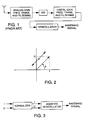
- FIG. 1 is a block diagram of a prior art FM receiver, with signal demodulation and other functions performed by DSP.
- Analog front end circuitry processes the signal received at the antenna and inputs the processed analog signal to an analog-to-digital converter (A/D), which digitises the signal.
- the analog processing may include gain, frequency translation, and filtering.
- the digital output of the A/D converter is processed by DSP circuitry that may perform gain, frequency translation and filtering functions in the digital domain to isolate the signal in the desired receiver channel.
- the desired signal is then input to the FM demodulator, which outputs the baseband signal, which is the FM composite signal for standard FM broadcast.
- FM can be described mathematically as phase modulation of a carrier by the integral of the modulating (or baseband) signal, as discussed in Solid State Radio Engineering , by Krauss, Bostian, and Raab, published by John Wiley and Sons, 1980.
- the demodulation process for FM can be described as the derivative of the phase of the modulated carrier.
- a single carrier in complex form can be represented diagrammatically as a single phasor in the real-imaginary signal plane, with the real and imaginary coordinates of the phasor's tip equal to I and Q respectively, as shown in Figure 2.
- the magnitude M of the carrier is the length of the phasor, and the phase of the carrier is the angle P from the real axis, as shown.
- one prior art FM demodulation scheme is to calculate the phase equal to the arctangent of Q divided by I, then take the derivative of the phase to obtain the baseband signal.
- the denominator of (1) is the square of the magnitude of the carrier phasor.
- Equation (2) can be viewed as the modified demodulator.
- the magnitude of the phasor formed by I l (t) and Q l (t) is exactly l due to the value of K.
- multiplying I(t) and Q(t) by K to obtain I l (t) and Q l (t) in effect "normalizes" the phasor to magnitude l. This removes any amplitude variation of the carrier phasor, and thus performs the same function as a limiter in an analog FM demodulator.
- the demodulation process thus consists of normalising the complex signal, then using the modified demodulator to demodulate the normalised signal, as shown in Figure 3. Normalisation is performed by calculating K as defined above, and then multiplying I and Q by K.
- the derivatives in (2) (as well as in (l)), can be calculated using known methods, such as FIR or IIR filter structures.
- K can be calculated from a polynomial function of I2 + Q2.
- the square root of (I2 + Q2) can be calculated using a square-root algorithm, such as a polynomial algorithm or Booth's algorithm.
- K can be calculated using a 1/x function, such as binary long division.
- Still another method is to use Newton-Raphson iteration. In terms of hardware or software implementations, all of these approaches require an excessive amount of processing power to obtain K.
- a method and apparatus which arrives at a value of K in a iterative manner, which in relation to the prior art requires a smaller amount of processing power, thus reducing the cost of implementing the function.
- the normaliser comprises a first stage generally designated 10 that performs a coarse normalisation on the inputs I1 and Q1 to produce I2 and Q2 so that the absolute value of at least one of the outputs is equal to or greater than 0.25 and the absolute value of each output is less than 0.5.
- the digital multi-bit words I1 and Q1 are parallel loaded into shift registers 12 and 14 respectively under the control of load signal LD1 at a rate of f1, where f1 is the sample rate of the system.
- the shift control logic 15 shifts the bits in the registers 12 and 14 under control of clock signals CLK2 and also performs the logic necessary to detect the intermediate shifted values of I1 and Q1 and stop shifting when the absolute value of the I1 and Q1 meet the condition set out above.
- the results of this shifting operation are loaded into registers 16 and 18 at rate f1, by a clock signal CLK1.
- I1 and Q1 are shifted left or right a bit at a time until: L 2 ⁇
- the limits in (3) to (6) are integer powers of 2. This allows the range checking associated with the coarse normalisation to be performed by directly checking the three most significant bits (MSBs) of I2 and Q2. Arbitrary limits could be used, but absolute-value functions and full comparators would be needed in that case.
- the maximum limit of each of I2 and Q2 is less than L (up to but not including L), then at least one of these two signals will be ⁇ L/2, due to the fact that the coarse normalisation is performed by bit shifting.
- Registers 16 and 18 are provided to store I2 and I3 respectively, to insure that I2 and Q2 are available to subsequent processing for the full length of the sample period 1/f1. If I1 and Q1 each have N1 bits resolution, no more than N1 - 1 shifts will be needed.
- a second stage In a second stage generally designated 20, the outputs of the first stage I2 and Q2 are respectively squared by multipliers 22 and 24 and summed in adder 26.
- the range in (8) is a mathematical result of the range on I2 and Q2, and the number system used.
- the upper limit of each of I2 and Q2 is L- ⁇
- the upper limit of A occurs when both I2 and Q2 are at their upper limit
- the upper limit of A is 2(L- ⁇ )2.
- the lower limit of A occurs when one of I2 or Q2 is at its lower limit L/2, and the other signal is 0, so the lower limit of A is (L/2)2.
- L 1.0
- A can exceed 1.0, which is outside the limits of the number system.
- L 0.5 as stated above, A will not exceed 1.0.
- the digital multi-bit word A is input to a third stage generally designated 28 shown in Figure 4b.
- the K register has NK bits, numbered from NK-1 (MSB) to 0 (LSB).
- K 0 ⁇ K ⁇ 1.
- A 0.0625
- K the largest fractional value available. Since K is known to be positive, no sign-bit need be present in K. The details of the iterative process will be described hereinafter in detail.
- the final value of K is clocked into register 32, so that it is available for one complete sample period.
- a fourth stage ( Figure 4a) generally designated 33, the final outputs I3 and Q3 are calculated, as follows, and with the indicated order of operations to limit all numbers to within the number system.
- Registers 34, 36, 38, and 40 are for time alignment of I2 and Q2 with the K output from Register 32.
- Registers 42 and 44 provide storage for the results of multipliers 46 and 48 respectively.
- the multiply by 4 operation, in (17) and (18) is performed by taking the proper bits from the intermediate values KI2 and KQ2 as provided at the outputs of multipliers 46 and 48.
- circuitry is included at the input of register 42 to compare the output of the multiplier 46 with the value 0.25 and if equal thereto, to load the value 1.0 - ⁇ into the register 42, as required for the number system.
- An identical process is used with multiplier 48 and register 44.
- the iteration process determines the correct value of K one bit at a time, beginning with the most significant bit.
- the initial value of K in the register 30 is 0.
- (K2)A is calculated in an indirect manner that does not require multiplication.
- the value of K that is used assumes that the bit being determined in the iteration is equal to logic 1.
- (K2)A is ⁇ 0.0625, the bit in question in register 30 is actually set, otherwise, the bit is left clear.
- J as the current iteration, with J running from 0 to NK-1.
- shr M indicates a shift right operation by M bits, which in effect multiplies the affected value by 0.5 M .
- the logic 28 implements equations (17) and (18).
- the multi-bit word A is loaded into registers 50 and 52 when the load input LD is enabled by the timing signal LD2. After loading register 50 with A, it's content is shifted one bit to the right by CLK3.
- the clock signal CLK3 is preferable K times the frequency of CLK1 so that one iteration occurs each CLK3 pulse.
- a J counter 58 clocked from CLK3, counts the number of iteration performed, counting from 0 to NK-1.
- the content of the register 50 after being shifted right by one bit position for each iteration, provides one of the multi-bit inputs to an adder 54 which outputs X temp .
- the other input to the adder 54 is the output of an X register 56 which stores a previous output of the adder 54 as will be explained hereinafter.
- the output of the register 52 after being shifted right by two bit positions for each iteration by CLK3, provides one of the multi-bit inputs to an adder 60.
- the connections from the inputs of the adder 60 to the register 52 are offset by two bit positions to achieve a further multiplication of value A prior to addition to output of a barrel shifter 62, which provides the other input to the adder 60.
- the barrel shifter 62 receives and shifts the contents of X register 56 to the right by a number of bit positions equal to the value of the J counter 58.
- the output of the adder 60 provides one input to an adder 66 which outputs Y temp .
- the other input to the adder 66 is the output of a Y register 68.
- the Y register 68 is loaded with the output of the adder 66 and the X register 56 is loaded with the output of the adder 54 by a timing signal CLKxy.
- CLKxy is derived from CLK3 through an AND gate 70 which is enabled whenever the output of the adder 66 is ⁇ 0.0625 as determined by the comparator 72.
- the X register 56 and the Y register 68 are updated with X temp and Y temp respectively from the adders 54 and 66, and the bit NK-J-1 is set in the K register 30 through bit set control logic 74. If the output of adder 66 is greater than 0.0625 no update of the registers 56 and 68 occurs and the bit in bit position NK-J-1 is not set. When the iterative process begins the X register 56 and Y register 68 are cleared, the J counter 58 is set to 0 and the K register 30 is set to 0.
- the K register 30 is a 16 bit register then during the first iteration the value calculated by the adder 66 is checked and the most significant bit of the K register 30, i.e. the 15th bit position, is set if the output of the adder 66 is ⁇ 0.0625. On the second iteration the J counter 58 is incremented and the 14th bit position is either set or cleared depending on the value of the adder 66.
- stage 28 The steps performed in stage 28 may be summarised as follows:
- FIG. 5a and 5b a second embodiment of the invention is shown. Corresponding components from Figures 4a and 4b are designated with prime numbers in Figure 5a and 5b.
- the method of Figure 5 adds an extra stage of computation to shift A up one bit at a time to obtain A2, where 0.5 ⁇ A2 ⁇ 1.0. This allow the elements in the iteration stage 28' to have less bits.
- the shifting of A means that I2 and Q2 must be adjusted accordingly.
- the logic for coarse normalisation of A to produce A2 is generally designated 76 and includes a range detect block 78 which select the proper number of bit position shifts in a multiplexer 80 needed to bring A into the desired A2 range.
- the two bit code is stored in register 82 and is used to select the proper input for the multiplexer 84 to apply as a multiplier input to the multipliers 86 and 88 to adjust I2 and Q2. These inputs are 0.5 for Case 2, 0.5 sqrt(2) for Case 3 and 1 for Case 4.
- Registers 34' and 36' provide time alignment with the two bit value in the register 82.
- Registers 38' and 40' store the results of multipliers 86 and 88 for use by multipliers 46' and 48' and also provide time alignment with the K output from register 32.
- the multiply by 4 operations in (20) and (21) are performed by taking the proper bits from the intermediate values K(CI2) and K(CQ2).
Landscapes
- Engineering & Computer Science (AREA)
- Power Engineering (AREA)
- Complex Calculations (AREA)
- Circuits Of Receivers In General (AREA)
Applications Claiming Priority (2)
| Application Number | Priority Date | Filing Date | Title |
|---|---|---|---|
| US51919 | 1993-04-26 | ||
| US08/051,919 US5414735A (en) | 1993-04-26 | 1993-04-26 | Method and apparatus for normalizing components of a complex signal |
Publications (2)
| Publication Number | Publication Date |
|---|---|
| EP0622893A1 true EP0622893A1 (fr) | 1994-11-02 |
| EP0622893B1 EP0622893B1 (fr) | 1998-12-16 |
Family
ID=21974196
Family Applications (1)
| Application Number | Title | Priority Date | Filing Date |
|---|---|---|---|
| EP94302576A Expired - Lifetime EP0622893B1 (fr) | 1993-04-26 | 1994-04-12 | Procédé et appareil pour normaliser les composants d'un signal complexe |
Country Status (4)
| Country | Link |
|---|---|
| US (1) | US5414735A (fr) |
| EP (1) | EP0622893B1 (fr) |
| JP (1) | JPH076159A (fr) |
| DE (1) | DE69415207T2 (fr) |
Cited By (1)
| Publication number | Priority date | Publication date | Assignee | Title |
|---|---|---|---|---|
| EP1315324A1 (fr) * | 2001-11-21 | 2003-05-28 | Siemens Aktiengesellschaft | Procédé et dispositif permettant de determiner et commander de la puissance d'un signal digital complex d'abonné |
Families Citing this family (3)
| Publication number | Priority date | Publication date | Assignee | Title |
|---|---|---|---|---|
| JP3153869B2 (ja) * | 1993-05-11 | 2001-04-09 | 株式会社日立国際電気 | フェージング歪補償方式及びその回路 |
| JP2001069184A (ja) | 1999-08-31 | 2001-03-16 | Matsushita Electric Ind Co Ltd | リミッタ方法およびリミッタ装置 |
| EP3759883A4 (fr) * | 2018-03-01 | 2021-10-20 | Telefonaktiebolaget Lm Ericsson (Publ) | Procédés et appareil de démodulation de signal |
Citations (4)
| Publication number | Priority date | Publication date | Assignee | Title |
|---|---|---|---|---|
| US4592074A (en) * | 1984-06-01 | 1986-05-27 | Rockwell International Corporation | Simplified hardware implementation of a digital IF translator |
| US4675882A (en) * | 1985-09-10 | 1987-06-23 | Motorola, Inc. | FM demodulator |
| EP0343273A1 (fr) * | 1988-05-27 | 1989-11-29 | Deutsche ITT Industries GmbH | Circuit de correction pour une paire de signaux numériques en quadrature |
| EP0429948A2 (fr) * | 1989-11-15 | 1991-06-05 | Hitachi, Ltd. | Démodulateur pour un signal modulé en phase et récepteur de radio avec un tel démodulateur |
Family Cites Families (1)
| Publication number | Priority date | Publication date | Assignee | Title |
|---|---|---|---|---|
| US5230099A (en) * | 1991-01-24 | 1993-07-20 | Rockwell International Corporation | System for controlling phase and gain errors in an i/q direct conversion receiver |
-
1993
- 1993-04-26 US US08/051,919 patent/US5414735A/en not_active Expired - Fee Related
-
1994
- 1994-04-12 EP EP94302576A patent/EP0622893B1/fr not_active Expired - Lifetime
- 1994-04-12 DE DE69415207T patent/DE69415207T2/de not_active Expired - Fee Related
- 1994-04-25 JP JP6086501A patent/JPH076159A/ja active Pending
Patent Citations (4)
| Publication number | Priority date | Publication date | Assignee | Title |
|---|---|---|---|---|
| US4592074A (en) * | 1984-06-01 | 1986-05-27 | Rockwell International Corporation | Simplified hardware implementation of a digital IF translator |
| US4675882A (en) * | 1985-09-10 | 1987-06-23 | Motorola, Inc. | FM demodulator |
| EP0343273A1 (fr) * | 1988-05-27 | 1989-11-29 | Deutsche ITT Industries GmbH | Circuit de correction pour une paire de signaux numériques en quadrature |
| EP0429948A2 (fr) * | 1989-11-15 | 1991-06-05 | Hitachi, Ltd. | Démodulateur pour un signal modulé en phase et récepteur de radio avec un tel démodulateur |
Cited By (1)
| Publication number | Priority date | Publication date | Assignee | Title |
|---|---|---|---|---|
| EP1315324A1 (fr) * | 2001-11-21 | 2003-05-28 | Siemens Aktiengesellschaft | Procédé et dispositif permettant de determiner et commander de la puissance d'un signal digital complex d'abonné |
Also Published As
| Publication number | Publication date |
|---|---|
| DE69415207D1 (de) | 1999-01-28 |
| JPH076159A (ja) | 1995-01-10 |
| US5414735A (en) | 1995-05-09 |
| DE69415207T2 (de) | 1999-05-20 |
| EP0622893B1 (fr) | 1998-12-16 |
Similar Documents
| Publication | Publication Date | Title |
|---|---|---|
| US7103108B1 (en) | Digital signal processor transceiver | |
| EP0474615B1 (fr) | Procédé de l'élimination de la tension continue de décalage pour un radio-récepteur | |
| JP3283504B2 (ja) | Cordic複素数乗算器 | |
| US4061977A (en) | Phase tracking network | |
| EP0534384B1 (fr) | Annuleur d'interférence de polarisation croisée | |
| EP0111587B1 (fr) | Procédé et dispositif pour des opérations de division | |
| US5521559A (en) | Signal oscillator, FM modulation circuit using the same, and FM modulation method | |
| US5164962A (en) | Adaptive equalizer with midburst correction capability | |
| EP0736206B1 (fr) | Procede et appareil d'interpolation quadratique | |
| US5524026A (en) | Method and apparatus for judging timing phase of modem which is used in data communication | |
| EP0622893A1 (fr) | Procédé et appareil pour normaliser les composants d'un signal complexe | |
| US5382913A (en) | Method and apparatus for generating two phase-coherent signals with arbitrary frequency ratio | |
| US5917737A (en) | Fourier transform mechanization using one bit kernel function | |
| US20030161489A1 (en) | Digital attenuator | |
| JPH04290004A (ja) | 濾波装置 | |
| US4679210A (en) | Soft-limited digital pulse compressor | |
| US6920188B1 (en) | Method and apparatus for processing a multiple-component wide dynamic range signal | |
| US5305243A (en) | Method and device for comparing two variable analogue signals | |
| JPH0310425A (ja) | トランスバーサルフィルタ制御回路 | |
| US6983012B1 (en) | Implementation of digital filter with reduced hardware | |
| US20050027771A1 (en) | System and method for approximating division | |
| US7139330B1 (en) | System for signal mixing and method thereof | |
| KR100192798B1 (ko) | 직각 위상 편이 복조기의 정합 필터 | |
| US10250416B2 (en) | Recursive difference filter realization of digital filters | |
| EP0650646A1 (fr) | Recepteur rake a double transmission pour liaison radio digitale entre un appareil radio fixe et un appareil radio mobile |
Legal Events
| Date | Code | Title | Description |
|---|---|---|---|
| PUAI | Public reference made under article 153(3) epc to a published international application that has entered the european phase |
Free format text: ORIGINAL CODE: 0009012 |
|
| AK | Designated contracting states |
Kind code of ref document: A1 Designated state(s): DE FR GB |
|
| 17P | Request for examination filed |
Effective date: 19950410 |
|
| 17Q | First examination report despatched |
Effective date: 19970506 |
|
| GRAG | Despatch of communication of intention to grant |
Free format text: ORIGINAL CODE: EPIDOS AGRA |
|
| GRAG | Despatch of communication of intention to grant |
Free format text: ORIGINAL CODE: EPIDOS AGRA |
|
| GRAH | Despatch of communication of intention to grant a patent |
Free format text: ORIGINAL CODE: EPIDOS IGRA |
|
| GRAH | Despatch of communication of intention to grant a patent |
Free format text: ORIGINAL CODE: EPIDOS IGRA |
|
| GRAA | (expected) grant |
Free format text: ORIGINAL CODE: 0009210 |
|
| AK | Designated contracting states |
Kind code of ref document: B1 Designated state(s): DE FR GB |
|
| REF | Corresponds to: |
Ref document number: 69415207 Country of ref document: DE Date of ref document: 19990128 |
|
| ET | Fr: translation filed | ||
| REG | Reference to a national code |
Ref country code: FR Ref legal event code: D6 |
|
| PLBE | No opposition filed within time limit |
Free format text: ORIGINAL CODE: 0009261 |
|
| STAA | Information on the status of an ep patent application or granted ep patent |
Free format text: STATUS: NO OPPOSITION FILED WITHIN TIME LIMIT |
|
| 26N | No opposition filed | ||
| REG | Reference to a national code |
Ref country code: GB Ref legal event code: IF02 |
|
| PGFP | Annual fee paid to national office [announced via postgrant information from national office to epo] |
Ref country code: DE Payment date: 20070423 Year of fee payment: 14 |
|
| PGFP | Annual fee paid to national office [announced via postgrant information from national office to epo] |
Ref country code: GB Payment date: 20070426 Year of fee payment: 14 |
|
| PGFP | Annual fee paid to national office [announced via postgrant information from national office to epo] |
Ref country code: FR Payment date: 20070416 Year of fee payment: 14 |
|
| GBPC | Gb: european patent ceased through non-payment of renewal fee |
Effective date: 20080412 |
|
| PG25 | Lapsed in a contracting state [announced via postgrant information from national office to epo] |
Ref country code: DE Free format text: LAPSE BECAUSE OF NON-PAYMENT OF DUE FEES Effective date: 20081101 |
|
| REG | Reference to a national code |
Ref country code: FR Ref legal event code: ST Effective date: 20081231 |
|
| PG25 | Lapsed in a contracting state [announced via postgrant information from national office to epo] |
Ref country code: FR Free format text: LAPSE BECAUSE OF NON-PAYMENT OF DUE FEES Effective date: 20080430 |
|
| PG25 | Lapsed in a contracting state [announced via postgrant information from national office to epo] |
Ref country code: GB Free format text: LAPSE BECAUSE OF NON-PAYMENT OF DUE FEES Effective date: 20080412 |