EP0624801A1 - Inspektionsapparat und -Verfahren, sowie Halbleiter - Google Patents
Inspektionsapparat und -Verfahren, sowie Halbleiter Download PDFInfo
- Publication number
- EP0624801A1 EP0624801A1 EP94105335A EP94105335A EP0624801A1 EP 0624801 A1 EP0624801 A1 EP 0624801A1 EP 94105335 A EP94105335 A EP 94105335A EP 94105335 A EP94105335 A EP 94105335A EP 0624801 A1 EP0624801 A1 EP 0624801A1
- Authority
- EP
- European Patent Office
- Prior art keywords
- transmission passage
- inspection apparatus
- electrode
- insulator
- semiconductor device
- Prior art date
- Legal status (The legal status is an assumption and is not a legal conclusion. Google has not performed a legal analysis and makes no representation as to the accuracy of the status listed.)
- Withdrawn
Links
Images








Classifications
-
- G—PHYSICS
- G01—MEASURING; TESTING
- G01R—MEASURING ELECTRIC VARIABLES; MEASURING MAGNETIC VARIABLES
- G01R1/00—Details of instruments or arrangements of the types included in groups G01R5/00 - G01R13/00 and G01R31/00
- G01R1/02—General constructional details
- G01R1/06—Measuring leads; Measuring probes
- G01R1/067—Measuring probes
- G01R1/06772—High frequency probes
Definitions
- the present invention relates to an inspection apparatus for inspecting the high frequency characteristics of a high frequency semiconductor device, an inspection method of inspecting a high frequency semiconductor device with the use of the inspection apparatus above-mentioned, and a high frequency semiconductor device to be inspected with the inspection apparatus above-mentioned.
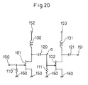
- Fig. 20 shows the high frequency amplifying circuit above-mentioned, which has field-effect transistors (hereinafter referred to as FETs) 101, 102, and resistors 110, 111.
- FETs field-effect transistors
- resistors 110, 111 the gate-source bias voltages of the FETs 101, 102 are set to 0 V.
- Capacitors 120, 121 are disposed for interrupting a low frequency component and a direct current component of a signal, thereby to transmit only a high frequency component thereof.
- Inductors 130, 131 are disposed for giving a direct current to the FETs 101, 102 and for preventing a high frequency signal (RF signal) from escaping to the power source side.
- RF signal high frequency signal
- the high frequency amplifying circuit is roughly divided by a point a into two portions, i.e., a front-stage block which is located in the left hand with respect to the point a and a rear-stage block which is located in the right hand with respect to the point a .
- a power voltage As a power voltage, 5.0 V is given to the power source terminals 152, 153 so that an electric current is supplied to the FETs 101, 102.
- the gate-source bias voltages are fixed to 0 V by the resistors 110, 111.
- the following description will discuss a high frequency semiconductor device having, on a semiconductor substrate, the high frequency amplifying circuit having the arrangement above-mentioned.
- Fig. 21 shows a high frequency semiconductor device 200 of the type above-mentioned. Shown in Fig. 21 are a FET 201 corresponding to the FET 101 shown in Fig. 20, a FET 202 corresponding to the FET 102, a resistor 210 corresponding to the resistor 110, a resistor 211 corresponding to the resistor 111, a capacitor 220 corresponding to the capacitor 120, an inductor 230 corresponding to the inductor 130, and an inductor 231 corresponding to the inductor 131. There are also disposed an input pad 250 corresponding to the RF signal input terminal 150 shown in Fig.
- the capacitor 220 is an MIM (Metal Insulator Metal) capacitor formed by a first wiring metallic layer formed on the semiconductor substrate, an insulator layer formed on the first wiring metallic layer and a second wiring metallic layer formed on the insulator layer.
- the second wiring metallic layer serves as an upper electrode.
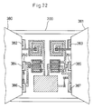
- Fig. 22 shows a conventional RF inspection method of inspecting the high frequency semiconductor device 200.
- probes 380, 381 are high frequency measuring probes manufactured by Cascade Microtech (hereinafter referred to simply as high frequency probes).
- the high frequency probe 380 has a power source contact electrode 382, an input contact electrode 384 and a grounding contact electrode 386.
- the high frequency probe 381 has a power source contact electrode 383, an output contact electrode 385 and a grounding contact electrode 387.
- the high frequency probes 380, 381 are designed such that a characteristic impedance of 50 ⁇ is held up to the tips thereof.
- the input/output characteristics of the entire high frequency amplifying circuit of the high frequency semiconductor device 200 can be accurately evaluated in the following manner.
- the respective electrodes of the high frequency probes 380, 381 are contacted with the corresponding pads of the high frequency semiconductor device 200, a signal is entered from the input contact electrode 384 of the high frequency probe 380 into the input pad 250 of the high frequency semiconductor device 200, a signal supplied from the output pad 251 of the high frequency semiconductor device 200 is received by the output contact electrode 385 of the high frequency probe 381, and the signal from the output pad 251 is measured.
- a pad is connected to that portion of the high frequency semiconductor device 200 which corresponds to the point a in Fig. 20, and the electrode of a high frequency probe is contacted with the pad, thereby to evaluate the characteristics of each block.
- the present invention is proposed with the object of providing an inspection apparatus for and an inspection method of accurately inspecting the characteristics of respective parts of the circuit of a semiconductor device, and also providing a semiconductor device to be suitably inspected with the inspection apparatus above-mentioned or by the inspection method above-mentioned.
- a first inspection apparatus comprises: an insulator substrate made of a material having a high dielectric constant; a signal transmission passage made of an electrically conductive material and formed on the top surface of the insulator substrate; a grounding electrode made of an electrically conductive material and formed at least on the top surfaces of those portions of the insulator substrate which are opposite to each other with another portion of the insulator substrate where the signal transmission passage is disposed held therebetween; a microstrip line formed by the signal transmission passage and those portions of the grounding electrode which are opposite to each other with the signal transmission passage held therebetween; and a detecting electrode made of an electrically conductive material and formed at the underside of the insulator substrate, the detecting electrode being electrically connected to the signal transmission passage through a through-hole formed in the insulator substrate.
- the detecting electrode when the detecting electrode is contacted with an insulator protective layer on an MIM capacitor of a semiconductor device, the detecting electrode, the insulator protective layer and an upper metallic layer of the MIM capacitor serve as a capacitor, so that the detecting electrode can receive a high frequency signal from the MIM capacitor. Also, the detecting electrode can supply a high frequency signal to the MIM capacitor of the semiconductor device. It is therefore possible to inspect the characteristics of each of the blocks and FETs of the circuit of the semiconductor device. Further, by matching the characteristic impedance of the microstrip line with the characteristic impedance of a measuring system, high frequency signals at connection parts of the circuit of the semiconductor device can accurately be measured. Accordingly, the semiconductor device inspection precision can be enhanced.
- the signal transmission passage may be divided into first, second and third partial transmission passages
- the microstrip line may have (i) a capacitor having one electrode electrically connected to the first partial transmission passage and the other electrode electrically connected to the second partial transmission passage, and (ii) a transistor of which each electrode is electrically connected, by wire bonding, to the grounding electrode, the second partial transmission passage or the third partial transmission passage, the transistor being adapted to amplify a high frequency signal.
- the capacitor is connected in series to the inside of the signal transmission passage, and the high frequency amplifying transistor is connected, by wire bonding, to the grounding electrode and the signal transmission passage.
- the signal transmission passage may be divided into first, second and third partial transmission passages
- the microstrip line may have (i) a capacitor having one electrode electrically connected to the first partial transmission passage and the other electrode electrically connected to the second partial transmission passage, and (ii) a transistor of which each electrode is electrically connected, by flip chip bonding, to the grounding electrode, the second partial transmission passage or the third partial transmission passage, the transistor being adapted to amplify a high frequency signal.
- the capacitor is connected in series to the inside of the signal transmission passage, and the high frequency amplifying transistor is connected, by flip chip bonding, to the grounding electrode and the signal transmission passage.
- each of the one and the other electrodes of the capacitor may comprise a metallic layer
- the capacitor may be an MIM capacitor comprising the metallic layers and an insulator layer made of a material having a high dielectric constant and interposed between the metallic layers. According to the arrangement above-mentioned, there can be achieved an inspection apparatus excellent in frequency characteristics.
- a second inspection apparatus comprises: an insulator substrate made of a material having a high dielectric constant; a signal transmission passage made of an electrically conductive material and formed inside of the insulator substrate; a detecting electrode made of an electrically conductive material and formed at the underside of the insulator substrate, the detecting electrode being electrically connected to the signal transmission passage through an introduction hole which is formed in the insulator substrate and which extends from the underside to the inside thereof; a first grounding electrode made of an electrically conductive material and formed on the entire top surface of the insulator substrate; and a second grounding electrode made of an electrically conductive material and formed at the entire underside of the insulator substrate except for its portion where the detecting electrode is disposed and for its portion adjacent to the first-mentioned portion.
- the detecting electrode when the detecting electrode is contacted with an insulator protective layer on an MIM capacitor of a semiconductor device, the detecting electrode, the insulator protective layer and an upper metallic layer of the MIM capacitor serve as a capacitor, so that the detecting electrode can receive a high frequency signal from the MIM capacitor. Also, the detecting electrode can supply a high frequency signal to the MIM capacitor of the semiconductor device. It is therefore possible to inspect the characteristics of each of the blocks and FETs of the circuit of the semiconductor device. Further, the first and second grounding electrodes at the top and underside of the insulator substrate prevent a noise signal from entering into the signal transmission passage from the outside of the second inspection apparatus. This increases the purity of a signal entered in or supplied from the detecting electrode, thus enhancing the semiconductor device inspection precision.
- the signal transmission passage may be divided into first, second and third partial transmission passages, and the inspection apparatus may comprise: a capacitor having one electrode electrically connected to the first partial transmission passage and the other electrode electrically connected to the second partial transmission passage; and a transistor of which each electrode is electrically connected, by wire bonding, to the first grounding electrode, the second grounding electrode, the second partial transmission passage or the third partial transmission passage, the transistor being adapted to amplify a high frequency signal.
- the capacitor is connected in series to the inside of the signal transmission passage, and the high frequency amplifying transistor is connected, by wire bonding, to the first and second grounding electrodes and the signal transmission passage.
- the signal transmission passage may be divided into first, second and third partial transmission passages, and the inspection apparatus may further comprise: a capacitor having one electrode electrically connected to the first partial transmission passage and the other electrode electrically connected to the second partial transmission passage; and a transistor of which each electrode is electrically connected, by flip chip bonding, to the first grounding electrode, the second grounding electrode, the second partial transmission passage or the third partial transmission passage, the transistor being adapted to amplify a high frequency signal.
- the capacitor is connected in series to the inside of the signal transmission passage, and the high frequency amplifying transistor is connected, by flip chip bonding, to the first and second grounding electrodes and the signal transmission passage.
- the present invention provides a first semiconductor device comprising: an MIM capacitor having a first metallic layer formed on a semiconductor substrate, an insulator layer formed on the first metallic layer and a second metallic layer formed on the insulator layer; an insulator protective layer formed on the MIM capacitor; and an electrical conductor layer made of an electrically conductive material and formed on the insulator protective layer.
- the second metallic layer of the MIM capacitor, the insulator protective layer on the second metallic layer and the electrical conductor layer on the insulator protective layer form a capacitor. Accordingly, when inspecting the characteristics of the first semiconductor device, a stable signal value can be obtained to improve the inspection in accuracy.
- a second semiconductor device comprises: a wiring layer formed on a semiconductor substrate; an insulator protective layer formed on the wiring layer; and an electrical conductor layer made of an electrically conductive material and formed on the insulator protective layer.
- the wiring layer, the insulator protective layer on the wiring layer and the electrical conductor layer on the insulator protective layer form a capacitor. Accordingly, when inspecting the characteristics of the second semiconductor device, a stable signal value can be obtained to improve the inspection in accuracy.
- the present invention provides a first inspection method of inspecting a semiconductor device with the use of the first or second inspection apparatus according to the present invention, in which the semiconductor device comprises (i) an MIM capacitor having a first metallic layer formed on a semiconductor substrate, an insulator layer formed on the first metallic layer and a second metallic layer formed on the insulator layer, and (ii) an insulator protective layer formed on the MIM capacitor, and in which, with the detecting electrode of the inspection apparatus brought close to or contacted with the insulator protective layer of the semiconductor device, the detecting electrode of the inspection apparatus is adapted to supply or receive a high frequency signal to or from the MIM capacitor of the semiconductor device, so that the high frequency characteristics of the semiconductor device are inspected.
- the detecting electrode of the inspection apparatus when the detecting electrode of the inspection apparatus is brought close to or contacted with the insulator protective layer on the MIM capacitor of the semiconductor device, the detecting electrode, the insulator protective layer and the second metallic layer of the MIM capacitor form a capacitor.
- This enables a high frequency signal to be transmitted between the circuit of the semiconductor device and the detecting electrode of the inspection apparatus.
- the detecting electrode of the inspection apparatus can supply or receive a high frequency signal to or from the MIM capacitor of the semiconductor device, so that the high frequency characteristics of the respective portions of the circuit of the semiconductor device can be inspected.
- the present invention also provides a second inspection method of inspecting a semiconductor device with the use of the first or second inspection apparatus according to the present invention, in which the semiconductor device comprises a wiring layer formed on a semiconductor substrate and an insulator protective layer formed on the wiring layer, and in which, with the detecting electrode of the inspection apparatus brought close to or contacted with the insulator protective layer of the semiconductor device, the detecting electrode of the inspection apparatus is adapted to supply or receive a high frequency signal to or from the wiring layer of the semiconductor device, so that the high frequency characteristics of the semiconductor device are inspected.
- the detecting electrode of the inspection apparatus when the detecting electrode of the inspection apparatus is brought close to or contacted with the insulator protective layer on the wiring layer of the semiconductor device, the detecting electrode, the insulator protective layer and the wiring layer form a capacitor. This enables a high frequency signal to be transmitted between the circuit of the semiconductor device and the detecting electrode of the inspection apparatus. In such a state, the detecting electrode of the inspection apparatus can supply or receive a high frequency signal to or from the wiring layer of the semiconductor device, so that the high frequency characteristics of the respective portions of the circuit of the semiconductor device can be inspected.
- the present invention also provides a third inspection method of inspecting the first semiconductor device according to the present invention with the use of the first or second inspection apparatus according to the present invention, in which, with the detecting electrode of the inspection apparatus brought close to or contacted with the electrical conductor layer of the first semiconductor device, the detecting electrode of the inspection apparatus is adapted to supply or receive a high frequency signal to or from the MIM capacitor of the first semiconductor device, so that the high frequency characteristics of the first semiconductor device are inspected.
- the present invention also provides a fourth inspection method of inspecting the second semiconductor device according to the present invention with the use of the first or second inspection apparatus according to the present invention, in which, with the detecting electrode of the inspection apparatus brought close to or contacted with the electrical conductor layer of the second semiconductor device, the detecting electrode of the inspection apparatus is adapted to supply or receive a high frequency signal to or from the wiring layer of the second semiconductor device, so that the high frequency characteristics of the second semiconductor device are inspected.
- the detecting electrode of the inspection apparatus can be reduced in wear as compared with a method in which the detecting electrode is contacted directly with the insulator protective layer of the semiconductor device.
- a semiconductor device to be inspected is similar to the high frequency semiconductor device 200 shown in Fig. 21.
- Fig. 1 (a) and Fig. 1 (b) show an inspection apparatus 10 according to the first embodiment.
- Fig. 1 (a) is a plan view
- Fig. 1 (b) is a section view taken along the line A-A in Fig. 1 (a).
- a grounding electrode 11 there are disposed a grounding electrode 11, a signal transmission passage 12, a through-hole 13, a detecting electrode 14 and a ceramic supporting substrate 15.
- the signal transmission passage 12 transversely extends over the top surface of the ceramic supporting substrate 15.
- the grounding electrode 11 is disposed on the entire top surface of the ceramic supporting substrate 15 except for its portion where the signal transmission passage 12 is disposed and for its portion adjacent to the first-mentioned portion.
- the detecting electrode 14 is disposed at the underside of the left-end portion of the ceramic supporting substrate 15, and a microstrip line is formed by the signal transmission passage 12 and those portions of the grounding electrode 11 which are opposite to each other with the signal transmission passage 12 held therebetween.
- Each of the grounding electrode 11, the signal transmission passage 12 and the detecting electrode 14 is made of an alloy containing 90 % or more of gold, and the detecting electrode 14 is improved in wear resistance in that the surface thereof is coated with a tungsten alloy of 20 ⁇ m in thickness.
- the signal transmission passage 12 and the detecting electrode 14 are connected to each other by an alloy of the type above-mentioned through the through-hole 13 formed in the left-end portion of the ceramic supporting substrate 15.
- FIG. 2 which shows the inspection method above-mentioned, there is shown an inspection apparatus 10 according to the first embodiment, having a detecting electrode 14.
- a high frequency semiconductor device 200 is similar to the device shown in Fig. 21 and has an MIM capacitor 220, an input pad 250 and an output pad 251.
- the high frequency probe 380 has a power source contact electrode 382, an input contact electrode 384 and a grounding contact electrode 386.
- the high frequency probe 381 has a power source contact electrode 383, an output contact electrode 385 and a grounding contact electrode 387.
- the input contact electrode 384 of the high frequency probe 380 is contacted with the input pad 250 of the high frequency semiconductor device 200
- the output contact electrode 385 of the high frequency probe 381 is contacted with the output pad 251 of the high frequency semiconductor device 200
- the detecting electrode 14 of the inspection apparatus 10 is contacted with an insulator protective layer on a second wiring metallic layer serving as an upper electrode of the capacitor 220 of the high frequency semiconductor device 200.
- Fig. 3 is a section view taken along the line B-B in Fig. 2.
- the inspection apparatus 10 according to the first embodiment, which has a grounding electrode 11, a signal transmission passage 12, a through-hole 13, the detecting electrode 14 and a ceramic supporting substrate 15.
- a high frequency semiconductor device 200 is similar to the device shown in Fig.
- insulator 21 has a semiconductor substrate 221, a first wiring metallic layer 222 formed on the semiconductor substrate 221, an insulator layer 224 formed as extending from the first wiring metallic layer 222 onto the semiconductor substrate 221, a second wiring metallic layer 223 formed on the insulator layer 224, and an MIM capacitor 220 formed by (i) the first wiring metallic layer 222, (ii) the second wiring metallic layer 223 and (iii) that portion of the insulator layer 224 which is interposed between the first and second wiring metallic layers.
- An insulator protective layer 225 is formed as extending from the MIM capacitor 220 onto the insulator layer 224.
- the detecting electrode 14 of the inspection apparatus 10 is disposed on the insulator protective layer 225 on the second wiring metallic layer 223 of the high frequency semiconductor device 200. Accordingly, the second wiring metallic layer 223, the detecting electrode 14 and that portion of the insulator protective layer 225 interposed between the second wiring metallic layer 223 and the detecting electrode 14, serve as an MIM capacitor, and a portion of an RF signal electric power at that portion of the high frequency semiconductor device 200 which is opposite to the point a shown in Fig. 20, is supplied to the detecting electrode 14 of the inspection apparatus 10.
- the characteristics of the front-stage block of the high frequency amplifying circuit in the high frequency semiconductor device 200 there can be obtained the characteristics of the front-stage block of the high frequency amplifying circuit in the high frequency semiconductor device 200.
- the characteristics of the rear-stage block of the high frequency amplifying circuit when an RF signal is entered from the detecting electrode 14 of the inspection apparatus 10 into the MIM capacitor 220 of the high frequency semiconductor device 200 and the RF signal electric power at the output pad 251 of the high frequency semiconductor device 200 is measured with the operation of the front-stage block of the high frequency amplifying circuit stopped.
- the detecting electrode 14 is contacted with the insulator protective layer 225 on the MIM capacitor 220 in the high frequency semiconductor device 200, so that the detecting electrode 14, the insulator protective layer 225 and the second wiring metallic layer 223 of the MIM capacitor 220, serve as a capacitor, and the detecting electrode 14 can therefore receive the RF signal from the MIM capacitor 220.
- an RF signal can be supplied from the detecting electrode 14 to the MIM capacitor 220 of the high frequency semiconductor device 200. It is therefore possible to inspect the characteristics of each of the blocks forming the high frequency amplifying circuit of the high frequency semiconductor device 200.
- the characteristic impedance of the microstrip line is matched with the characteristic impedance of the measuring system, there can be accurately measured the RF signal at each connection part in the high frequency amplifying circuit of the high frequency semiconductor device 200. This improves the precision at which the high frequency semiconductor device 200 is inspected.
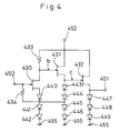
- Fig. 4 shows a high frequency amplifying circuit of the high frequency semiconductor device above-mentioned. Shown in Fig. 4 are FETs 430, 431, 432, resistors 433, 434, diodes 440 to 449, an RF signal input terminal 450, an RF signal output terminal 451, a power source terminal 452, and grounding terminals 455.
- 5.0 V is given, as a power voltage, to the power source terminal 452, so that an electric current is supplied to the FETs 430 to 432.
- the respective FETs are designed such that the gate bias voltages are set to the optimum values by the resistor 433 and the diodes 440 to 449.
- the FET 431 has a source follower arrangement and serves as an output buffer.
- the FET 431 transmits the RF signal to the next-stage FET 432 and returns a portion of the RF signal back to the first-stage FET 430 through the resistor 434.
- the last-stage FET 432 serves as a buffer circuit of a source follower arrangement for restraining an influence of a circuit at the subsequent stage.
- Fig. 5 shows a high frequency semiconductor device 500 of the type above-mentioned. Shown in Fig. 5 are a FET 530 corresponding to the FET 430 shown in Fig. 4, a FET 531 corresponding to the FET 431, a FET 532 corresponding to the FET 432, a resistor 533 corresponding to the resistor 433, a resistor 534 corresponding to the resistor 434, and diodes 540 to 549 corresponding to the diodes 440 to 449. There are also disposed an input pad 550 corresponding to the RF signal input terminal 450 shown in Fig.
- Each of portions b and c in Fig. 5 is formed by a second wiring metallic layer and has a width equal to 30 ⁇ m which is three times or more as wide as the normal width.
- FIG. 6 which shows the inspection method above-mentioned, there are shown inspection apparatus 10A, 10B each of which is similar to the inspection apparatus 10 according to the first embodiment shown in Fig. 1 (a) and Fig. 1 (b), detecting electrodes 14A, 14B of the respective inspection apparatus 10A, 10B, and a high frequency semiconductor device 500 which has been shown in Fig. 5.
- the high frequency probe 380 has a power source contact electrode 382, an input contact electrode 384 and a grounding contact electrode 386.
- the high frequency probe 381 has a power source contact electrode 383, an output contact electrode 385 and a grounding contact electrode 387.
- the input contact electrode 384 of the high frequency probe 380 is contacted with the input pad 550 of the high frequency semiconductor device 500
- the output contact electrode 385 of the high frequency probe 381 is contacted with the output pad 551 of the high frequency semiconductor device 500
- the detecting electrode 14A of the inspection apparatus 10A is contacted with an insulator protective layer on the portion b of the second wiring metallic layer of the high frequency semiconductor device 500
- the detecting electrode 14B of the inspection apparatus 10B is contacted with the insulator protective layer on the portion c of the second wiring metallic layer of the high frequency semiconductor device 500.
- the detecting electrode 14A of the inspection apparatus 10A is disposed on the insulator protective layer on the portion b of the second wiring metallic layer of the high frequency semiconductor device 500
- the detecting electrode 14B of the inspection apparatus 10B is disposed on the insulator protective layer on the portion c of the second wiring metallic layer of the high frequency semiconductor device 500. Accordingly, (i) the portion b of the second wiring metallic layer of the high frequency semiconductor device 500, (ii) the detecting electrode 14A of the inspection apparatus 10A, and (iii) that portion of the insulator protective layer of the high frequency semiconductor device 500 which is interposed between the point b of the second wiring metallic layer and the detecting electrode 14A of the inspection apparatus 10A, serve as an MIM capacitor.
- the portion c of the second wiring metallic layer of the high frequency semiconductor device 500, (ii) the detecting electrode 14B of the inspection apparatus 10B and (iii) that portion of the insulator protective layer of the high frequency semiconductor device 500 which is interposed between the point c of the second wiring metallic layer and the detecting electrode 14B of the inspection apparatus 10B serve as an MIM capacitor.
- a signal is entered into the input pad 550 of the high frequency semiconductor device 500 from the input contact electrode 384 of the high frequency probe 380, a portion of an RF signal electric power at the portion b of the high frequency semiconductor device 500, is supplied to the detecting electrode 14A of the inspection apparatus 10A.
- the RF signal electric power there can be obtained the characteristics of the front-stage block of the high frequency amplifying circuit of the high frequency semiconductor device 500.
- an RF signal is entered from the detecting electrode 14A of the inspection apparatus 10A into the portion b of the high frequency semiconductor device 500, a portion of the RF signal electric power at the portion c of the high frequency semiconductor device 500 is received by the detecting electrode 14B of the inspection apparatus 10B, and the RF signal electric power is measured, there can be obtained the characteristics of the intermediate-stage block of the high frequency amplifying circuit of the high frequency semiconductor device 500.
- the detecting electrodes 14A, 14B of the inspection apparatus 10A, 10B are disposed on the insulator protective layer on the second wiring metallic layer of the high frequency semiconductor device 500. Accordingly, the detecting electrodes, the insulator protective layer and the second wiring metallic layer form the respective capacitors. This enables a high frequency signal to be transmitted between the high frequency amplifying circuit of the high frequency semiconductor device 500 and each of the inspection apparatus 10A, 10B.
- a semiconductor device to be inspected is similar to the high frequency semiconductor device 200 shown in Fig. 21.
- Fig. 7 (a) and Fig. 7 (b) show an inspection apparatus 20 of the third embodiment.
- Fig. 7 (a) is a plan view
- Fig. 7 (b) is a section view taken along the line C-C in Fig. 7 (a).
- a detecting electrode 21, grounding electrodes 22, 23, a signal transmission passage 24 and a multi-layer ceramic supporting substrate 25 there are disposed a detecting electrode 21, grounding electrodes 22, 23, a signal transmission passage 24 and a multi-layer ceramic supporting substrate 25.
- the signal transmission passage 24 transversely extends inside of the multi-layer ceramic supporting substrate 25.
- the detecting electrode 21 is disposed at the underside of the left-end portion of the multi-layer ceramic supporting substrate 25.
- the grounding electrode 22 is formed on the entire top surface of the multi-layer ceramic supporting substrate 25, and the grounding electrode 23 is formed at the entire underside of the multi-layer ceramic supporting substrate 25 except for its left-end portion.
- Each of the detecting electrode 21, the grounding electrodes 22, 23 and the signal transmission passage 24 is made of an alloy containing 90 % or more of gold, and the detecting electrode 21 is improved in wear resistance in that the surface thereof is coated with a tungsten alloy of 20 ⁇ m in thickness.
- the signal transmission passage 24 and the detecting electrode 21 are connected to each other by an alloy of the type above-mentioned through an introduction hole which is formed in the multi-layer ceramic supporting substrate 25 and which extends to the inside from the underside of the left-end portion of the multi-layer ceramic supporting substrate 25.
- Fig. 8 shows the inspection method according to the third embodiment, using an inspection apparatus 20 having the arrangement above-mentioned.
- the inspection apparatus 20 according to the third embodiment, a detecting electrode 21, a high frequency semiconductor device 200 similar to the device shown in Fig. 21, an MIM capacitor 220, an input pad 250 and an output pad 251.
- the high frequency probe 380 has a power source contact electrode 382, an input contact electrode 384 and a grounding contact electrode 386.
- the high frequency probe 381 has a power source contact electrode 383, an output contact electrode 385 and a grounding contact electrode 387.
- the input contact electrode 384 of the high frequency probe 380 is contacted with the input pad 250 of the high frequency semiconductor device 200
- the output contact electrode 385 of the high frequency probe 381 is contacted with the output pad 251 of the high frequency semiconductor device 200
- the detecting electrode 21 of the inspection apparatus 20 is contacted with an insulator protective layer on a second wiring metallic layer serving as an upper electrode of the capacitor 220 of the high frequency semiconductor device 200.
- the measuring principle in the third embodiment is similar to that in the first embodiment.
- the detecting electrode 21 of the inspection apparatus 20 is contacted with the insulator protective layer on the MIM capacitor 220 in the high frequency semiconductor device 200. Accordingly, the detecting electrode 21 of the inspection apparatus 20, the insulator protective layer of the high frequency semiconductor device 200 and the second wiring metallic layer of the MIM capacitor 220, serve as a capacitor. Therefore, the detecting electrode 21 of the inspection apparatus 20 can receive an RF signal from the MIM capacitor 220 of the high frequency semiconductor device 200. On the other hand, the detecting electrode 21 of the inspection apparatus 20 can supply an RF signal to the MIM capacitor 220 of the high frequency semiconductor device 200.
- the grounding electrodes 22, 23 at the top and underside of the multilayer ceramic supporting substrate 25, prevent a noise signal from entering into the signal transmission passage 24 from the outside of the inspection apparatus 20. This increases the purity of signals entered to and supplied from the detecting electrode 21 of the inspection apparatus 20, thus improving the precision at which the high frequency semiconductor device 200 is inspected.
- Fig. 9 (a) and Fig. 9 (b) show an inspection apparatus 30 of the fourth embodiment.
- Fig. 9 (a) is a plan view
- Fig. 9 (b) is a section view taken along the line D-D in Fig. 9 (a).
- grounding electrodes 31, 32 there are disposed grounding electrodes 31, 32, a signal transmission passage 33, a through-hole 34, a detecting electrode 35, a ceramic supporting substrate 36, a chip condenser 37, a semiconductor chip 40, bonding wires 38 and a light-shielding resin 39.
- the signal transmission passage 33 transversely extends on the top surface of the ceramic supporting substrate 36 and is divided into three partial transmission passages 33a, 33b, 33c.
- the grounding electrode 31 is disposed on the entire top surface of the ceramic supporting substrate 36 except for its portion where the signal transmission passage 33 is disposed, and for its portion adjacent to the first-mentioned portion.
- the detecting electrode 35 is disposed at the underside of the left-end portion of the ceramic supporting substrate 36, and the grounding electrode 32 is disposed at the entire underside of the ceramic supporting substrate 36 except for its left-end portion.
- Each of the grounding electrodes 31, 32, the signal transmission passage 33 and the detecting electrode 35 is made of an alloy containing 90 % or more of gold, and the detecting electrode 35 is improved in wear resistance in that the surface thereof is coated with a tungsten alloy of 20 ⁇ m in thickness.
- the partial transmission passage 33a and the detecting electrode 35 are connected to each other by an alloy of the type above-mentioned through the through-hole 34 formed in the left-end portion of the ceramic supporting substrate 36.
- the chip condenser 37 has one electrode electrically connected to the partial transmission passage 33a, and the other electrode electrically connected to the partial transmission passage 33b.
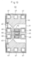
- Fig. 10 showing the semiconductor chip 40, there are shown a GaAs substrate 41, an FET 42, bias resistors 43, wiring metal 44 connected to the source electrode, wiring metal 45 connected to the drain electrode, wiring metal 46 connected to the gate electrode, source electrode pads 47, drain electrode pads 48, and gate electrode pads 49.
- the gate width is equal to 100 ⁇ m
- the chip sizes are 300 ⁇ m x 150 ⁇ m
- the substrate thickness is 50 ⁇ m.
- the semiconductor chip 40 is bonded to the ceramic supporting substrate 36 shown in Fig. 9 (a) and Fig. 9 (b).
- the gate electrode pads 49 are connected to the partial transmission passage 33b by wire bonding, the drain electrode pads 48 are connected, by wire bonding, to the partial transmission passage 33c adapted to be connected to an instrument, and the source electrode pads 47 are connected to the grounding electrode 31 by wire bonding.
- a signal detected by the detecting electrode 35 can be sent, as amplified by the semiconductor chip 40, to the instrument.
- the FET 42 is covered with the light-shielding resin 39 such that no influence is exerted to the FET 42 by external light.
- Fig. 11 shows a high frequency semiconductor device 600, which has the high frequency amplifying circuit shown in Fig. 4 formed in a usual wiring width on the semiconductor substrate thereof.
- Shown in Fig. 11 are FETs 630 to 632 corresponding to the FETs 430 to 432 shown in Fig. 4, resistors 633, 634 corresponding to the resistors 433; 434, diodes 640 to 649 corresponding to the diodes 440 to 449, an input pad 650 corresponding to the RF signal input terminal 450, an output pad 651 corresponding to the RF signal output terminal 451, power source pads 652, 653 corresponding to the power source terminal 452, and grounding pads 655 to 656 corresponding to the grounding terminals 455.
- each of portions d and e is formed by a second wiring metallic layer and has a usual wiring width of 10 ⁇ m.
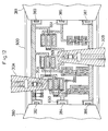
- Fig. 12 shows the inspection method according to the fourth embodiment of inspecting the high frequency semiconductor device 600 having the arrangement above-mentioned.
- inspection apparatus 30A, 30B each of which is similar to the inspection apparatus 30 according to the fourth embodiment shown in Fig. 9 (a) and Fig. 9 (b), detecting electrodes 35A, 35B of the respective inspection apparatus 30A, 30B, and the high frequency semiconductor device 600 which has been shown in Fig. 11.
- the high frequency probe 380 has a power source contact electrode 382, an input contact electrode 384 and a grounding contact electrode 386.
- the high frequency probe 381 has a power source contact electrode 383, an output contact electrode 385 and a grounding contact electrode 387.
- the input contact electrode 384 of the high frequency probe 380 is contacted with the input pad 650 of the high frequency semiconductor device 600
- the output contact electrode 385 of the high frequency probe 381 is contacted with the output pad 651 of the high frequency semiconductor device 600
- the detecting electrode 35A of the inspection apparatus 30A is contacted with an insulator protective layer on the portion d of the second wiring metallic layer of the high frequency semiconductor device 600
- the detecting electrode 35B of the inspection apparatus 30B is contacted with the insulator protective layer on the portion e of the second wiring metallic layer of the high frequency semiconductor device 600.
- the measuring principle is similar to that in the second embodiment.
- the chip condenser 37 is connected in series to the inside of the signal transmission passage 33, and the semiconductor chip 40 is connected to the grounding electrode 31 and the signal transmission passage 33 by wire bonding. This enables a weak voltage signal to be amplified, thus producing a signal of which signal/noise ratio (S/N ratio) is high. It is therefore possible to detect a signal on a signal line having a usual wiring width in the high frequency semiconductor device 600.
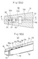
- Fig. 13 (a) and Fig. 13 (b) show an inspection apparatus 50 according to the fifth embodiment.
- Fig. 13 (a) is a plan view
- Fig. 13 (b) is a section view taken along the line E-E in Fig. 13 (a).
- the signal transmission passage 53 transversely extends on the top surface of the ceramic supporting substrate 56 and is divided into three partial transmission passages 53a, 53b, 53c.
- the grounding electrode 51 is disposed on the entire top surface of the ceramic supporting substrate 56 except for its portion where the signal transmission passage 53 is disposed, and for its portion adjacent to the first-mentioned portion.
- the detecting electrode 55 is disposed at the underside of the left-end portion of the ceramic supporting substrate 56, and the grounding electrode 52 is disposed at the entire underside of the ceramic supporting substrate 56 except for its left-end portion.
- Each of the grounding electrodes 51, 52, the signal transmission passage 53 and the Au bumps 58 is made of an alloy containing 90 % or more of gold, and the detecting electrode 55 is improved in wear resistance in that the surface thereof is coated with a tungsten alloy of 20 ⁇ m in thickness.
- the partial transmission passage 53a and the detecting electrode 55 are connected to each other by an alloy of the type above-mentioned through the through-hole 54 formed in the left-end portion of the ceramic supporting substrate 56.
- the chip condenser 57 has one electrode electrically connected to the partial transmission passage 53a, and the other electrode electrically connected to the partial transmission passage 53b.
- a GaAs substrate 61 there are disposed a GaAs substrate 61, an FET 62, bias resistors 63, wiring metal 64 connected to the source electrode, wiring metal 65 connected to the drain electrode, wiring metal 66 connected to the gate electrode, source electrode pads 67, drain electrode pads 68, gate electrode pads 69 and Au bumps 58 formed on the respective electrode pads.
- the gate width is equal to 100 ⁇ m
- the chip sizes are 300 ⁇ m x 150 ⁇ m
- the substrate thickness is 50 ⁇ m.
- the semiconductor chip 60 is bonded, under pressure, to the ceramic supporting substrate 56 while making sure of the position of the semiconductor chip 60 such that the gate electrode pads 69 are connected to the partial transmission passage 53b by Au bumps 58, that the drain electrode pads 68 are connected, by Au bumps 58, to the partial transmission passage 53c adapted to be connected to an instrument, and that the source electrode pads 67 are connected to the grounding electrode 51 by Au bumps 58.
- the semiconductor chip 60 is covered with the light-shielding resin 59 such that no influence is exerted to the chip 60 by external light.
- the chip condenser 57 is connected in series to the inside of the signal transmission passage 53, and the semiconductor chip 60 is connected to the grounding electrode 51 and the signal transmission passage 53 by flip chip bonding.
- FIG. 15 (a) and Fig. 15 (b) show an inspection apparatus 70 according to the sixth embodiment.
- Fig. 15 (a) is a plan view
- Fig. 15 (b) is a section view taken along the line F-F in Fig. 15 (a).
- Fig. 15 (a) and Fig. 15 (b) show an inspection apparatus 70 according to the sixth embodiment.
- Fig. 15 (a) is a plan view
- Fig. 15 (b) is a section view taken along the line F-F in Fig. 15 (a).
- grounding electrodes 71, 72 there are disposed grounding electrodes 71, 72, a signal transmission passage 73, a through-hole 74, a detecting electrode 75, a ceramic supporting substrate 76, an MIM capacitor 77, a semiconductor chip 60 similar to the semiconductor chip used in the inspection apparatus according to the fifth embodiment shown in Fig. 14, Au bumps 78 and a light-shielding resin 79.
- the signal transmission passage 73 transversely extends on the top surface of the ceramic supporting substrate 76 and is divided into three partial transmission passages 73a, 73b, 73c.
- the grounding electrode 71 is disposed on the entire top surface of the ceramic supporting substrate 76 except for its portion where the signal transmission passage 73 is disposed and for its portion adjacent to the first-mentioned portion.
- the detecting electrode 75 is disposed at the underside of the left-end portion of the ceramic supporting substrate 76, and the grounding electrode 72 is formed at the entire underside of the ceramic supporting substrate 76 except for its left-end portion.
- the MIM capacitor 77 has an insulator layer made of strontium titanate held by and between the right-end portion of the partial transmission passage 73a and the left-end portion of the partial transmission passage 73b, each of the partial transmission passages 73a, 73b serving as a metallic layer.
- Each of the grounding electrodes 71, 72, the signal transmission passage 73 and the detecting electrode 75 is made of an alloy containing 90 % or more of gold, and the detecting electrode 75 is improved in wear resistance in that the surface thereof is coated with a tungsten alloy of 20 ⁇ m in thickness.
- the partial transmission passage 73a and the detecting electrode 75 are connected to each other by an alloy of the type above-mentioned through the through-hole 74 formed in the left-end portion of the ceramic supporting substrate 76.
- the chip condenser 57 in the inspection apparatus 50 according to the fifth embodiment shown in Fig. 13 (a) and Fig. 13 (b), is replaced with the MIM capacitor 77.
- the inspection apparatus 70 according to the sixth embodiment there can be provided an inspection apparatus excellent in high frequency characteristics as compared with the arrangement using a chip condenser.
- FIG. 16 As an inspection apparatus, there is used apparatus similar to the inspection apparatus 10 according to the first embodiment shown in Fig. 1 (a) and Fig. 1 (b).
- Fig. 16 shows a semiconductor device 700 according to the seventh embodiment. Shown in Fig. 16 are FETs 701, 702, resistors 710, 711, and a capacitor 720 which is an MIM capacitor comprising a first wiring metallic layer formed on a semiconductor substrate, an insulator layer formed on the first wiring metallic layer and a second wiring metallic layer formed on the insulator layer, the second wiring metallic layer serving as an upper electrode. There are also disposed inductors 730, 731, an input pad 750, an output pad 751, power source pads 752, 753, grounding pads 760 and a metallic layer 770 formed on an insulator protective layer formed on the MIM capacitor 720.
- Fig. 17 shows an equivalent circuit of the semiconductor device 700 having the arrangement above-mentioned. Shown in Fig. 17 are FETs 801, 802 corresponding to the FETs 701, 702 shown in Fig. 16, and resistors 810, 811 corresponding to the resistors 710, 711. By these resistors 810, 811, the gate-source bias voltages in the FETs 801, 802 are set to 0 V. Capacitors 820, 821 are disposed for interrupting a low frequency component and a direct current component of a signal, causing only a high frequency component thereof to be transmitted. The capacitor 820 is corresponding to the MIM capacitor 720 shown in Fig. 16.
- Inductors 830, 831 correspond to the inductors 730, 731 shown in Fig. 16, and are disposed for giving a direct current to the FETs 801, 802 and for preventing a RF signal from escaping to the power source side. There are also disposed an RF signal input terminal 850 corresponding to the input pad 750 shown in Fig. 16, an RF signal output terminal 851 corresponding to the output pad 751, power source terminals 852, 853 corresponding to the power source pads 752, 753, grounding terminals 860 corresponding to the grounding pads 760 and an external terminal 854 corresponding to the metallic layer 770.
- a capacitor 822 comprises the second wiring metallic layer serving as the upper electrode of the MIM capacitor 720 shown in Fig. 16, the insulator protective layer on the second wiring metallic layer and the metallic layer 770 on the insulator protective layer.
- Fig. 18 which shows the inspection method above-mentioned, there are shown an inspection apparatus 10 similar to the inspection apparatus according to the first embodiment shown in Fig. 1 (a) and Fig. 1 (b), a detecting electrode 14, and the semiconductor device 700 according to the seventh embodiment. There are also shown the MIM capacitor 720, the metallic layer 770, the input pad 750, the output pad 751, and high frequency probes 380, 381.
- the high frequency probe 380 has a power source contact electrode 382, an input contact electrode 384 and a grounding contact electrode 386.
- the high frequency probe 381 has a power source contact electrode 383, an output contact electrode 385 and a grounding contact electrode 387.
- the input contact electrode 384 of the high frequency probe 380 is contacted with the input pad 750 of the high frequency semiconductor device 700
- the output contact electrode 385 of the high frequency probe 381 is contacted with the output pad 751 of the high frequency semiconductor device 700
- the detecting electrode 14 of the inspection apparatus 10 is contacted with the metallic layer 770 of the high frequency semiconductor device 700.
- the arrangement in Fig. 18 is equivalent to Fig. 17 when the detecting electrode 14 of the inspection apparatus 10 is connected to the external terminal 854 in Fig. 17.
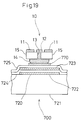
- Fig. 19 is a section view taken along the line G-G in Fig. 18.
- an inspection apparatus 10 similar to the inspection apparatus according to the first embodiment shown in Fig. 1 (a) and Fig. 1 (b), a grounding electrode 11, a signal transmission passage 12, a through-hole 13, a detecting electrode 14, a ceramic supporting substrate 15, and the high frequency semiconductor device 700 according to the seventh embodiment shown in Fig. 16.
- the high frequency semiconductor device 700 has a semiconductor substrate 721, a first wiring metallic layer 722 formed on the semiconductor substrate 721, an insulator layer 724 formed as extending from the first wiring metallic layer onto the semiconductor substrate 721, and a second wiring metallic layer 723 formed on the insulator layer 724.
- the MIM capacitor 720 is formed by (i) the first wiring metallic layer 722, (ii) the second wiring metallic layer 723 and (iii) that portion of the insulator layer 724 which is interposed between the first and second wiring metallic layers.
- An insulator protective layer 725 is formed as extending from the MIM capacitor 720 onto the insulator layer 724.
- the metallic layer 770 is formed on the insulator protective layer 725.
- the second wiring metallic layer 723 of the MIM capacitor 720 of the semiconductor device 700 serve as a capacitor. Accordingly, there can be obtained a more stabilized signal value as compared with the first embodiment, thus improving the inspection in accuracy.
- the inspection method of the seventh embodiment by contacting the detecting electrode 14 of the inspection apparatus 10 with the metallic layer 770 of the semiconductor device 700, there can be reduced a measurement error resulting from positional shift of the detecting electrode 14 of the inspection apparatus 10. Further, the inspection method of the seventh embodiment can reduce the detecting electrode 14 in wear as compared with a method in which the detecting electrode 14 of the inspection apparatus 10 comes in direct contact with the insulator protective layer 725 of the semiconductor device 700.
Landscapes
- Physics & Mathematics (AREA)
- General Physics & Mathematics (AREA)
- Testing Or Measuring Of Semiconductors Or The Like (AREA)
- Testing Of Individual Semiconductor Devices (AREA)
Applications Claiming Priority (2)
| Application Number | Priority Date | Filing Date | Title |
|---|---|---|---|
| JP5083566A JPH06295949A (ja) | 1993-04-09 | 1993-04-09 | 検査装置、検査方法及び半導体装置 |
| JP83566/93 | 1993-04-09 |
Publications (1)
| Publication Number | Publication Date |
|---|---|
| EP0624801A1 true EP0624801A1 (de) | 1994-11-17 |
Family
ID=13806070
Family Applications (1)
| Application Number | Title | Priority Date | Filing Date |
|---|---|---|---|
| EP94105335A Withdrawn EP0624801A1 (de) | 1993-04-09 | 1994-04-06 | Inspektionsapparat und -Verfahren, sowie Halbleiter |
Country Status (2)
| Country | Link |
|---|---|
| EP (1) | EP0624801A1 (de) |
| JP (1) | JPH06295949A (de) |
Cited By (7)
| Publication number | Priority date | Publication date | Assignee | Title |
|---|---|---|---|---|
| DE19603802A1 (de) * | 1995-02-03 | 1996-08-14 | Hewlett Packard Co | Spannungssonde mit Vielfachanschlußleitungen |
| EP0731360A3 (de) * | 1995-02-28 | 1997-07-16 | Plessey Semiconductors Ltd | Konstruktion zum Testen unbestückter integrierter Schaltungen |
| DE19718478A1 (de) * | 1997-04-30 | 1998-11-05 | Allice Mestechnik Gmbh | Prüfspitze für Hochimpedanzsonden mit extrem kleiner Eingangskapazität |
| EP0902293A1 (de) * | 1997-09-10 | 1999-03-17 | Soshotech Co., Ltd. | Kontaktsonde |
| EP1509776A4 (de) * | 2002-05-23 | 2010-08-18 | Cascade Microtech Inc | Sonde zum testen einer zu testenden einrichtung |
| EP1627235A4 (de) * | 2003-05-23 | 2010-08-18 | Cascade Microtech Inc | Sonde zum testen eines zu prüfenden bausteins |
| WO2011110255A3 (de) * | 2010-03-11 | 2012-01-05 | Rohde & Schwarz Gmbh & Co. Kg | Messspitze mit integriertem messwandler |
Families Citing this family (12)
| Publication number | Priority date | Publication date | Assignee | Title |
|---|---|---|---|---|
| US6232789B1 (en) | 1997-05-28 | 2001-05-15 | Cascade Microtech, Inc. | Probe holder for low current measurements |
| DE10143173A1 (de) | 2000-12-04 | 2002-06-06 | Cascade Microtech Inc | Wafersonde |
| US6724205B1 (en) | 2002-11-13 | 2004-04-20 | Cascade Microtech, Inc. | Probe for combined signals |
| JP4621414B2 (ja) * | 2003-03-13 | 2011-01-26 | 双信電機株式会社 | アンテナ測定装置及びアンテナ測定方法 |
| DE202004021093U1 (de) | 2003-12-24 | 2006-09-28 | Cascade Microtech, Inc., Beaverton | Aktiver Halbleiterscheibenmessfühler |
| KR20070058522A (ko) | 2004-09-13 | 2007-06-08 | 캐스케이드 마이크로테크 인코포레이티드 | 양측 프루빙 구조 |
| US7449899B2 (en) | 2005-06-08 | 2008-11-11 | Cascade Microtech, Inc. | Probe for high frequency signals |
| JP5080459B2 (ja) | 2005-06-13 | 2012-11-21 | カスケード マイクロテック インコーポレイテッド | 広帯域能動/受動差動信号プローブ |
| DE202007018733U1 (de) | 2006-06-09 | 2009-03-26 | Cascade Microtech, Inc., Beaverton | Messfühler für differentielle Signale mit integrierter Symmetrieschaltung |
| US7403028B2 (en) | 2006-06-12 | 2008-07-22 | Cascade Microtech, Inc. | Test structure and probe for differential signals |
| US7443186B2 (en) | 2006-06-12 | 2008-10-28 | Cascade Microtech, Inc. | On-wafer test structures for differential signals |
| WO2023228487A1 (ja) * | 2022-05-24 | 2023-11-30 | 株式会社村田製作所 | 測定ユニットおよび測定装置 |
Citations (3)
| Publication number | Priority date | Publication date | Assignee | Title |
|---|---|---|---|---|
| GB2197081A (en) * | 1986-11-07 | 1988-05-11 | Plessey Co Plc | Coplanar waveguide probe |
| US4894612A (en) * | 1987-08-13 | 1990-01-16 | Hypres, Incorporated | Soft probe for providing high speed on-wafer connections to a circuit |
| US4983910A (en) * | 1988-05-20 | 1991-01-08 | Stanford University | Millimeter-wave active probe |
-
1993
- 1993-04-09 JP JP5083566A patent/JPH06295949A/ja not_active Withdrawn
-
1994
- 1994-04-06 EP EP94105335A patent/EP0624801A1/de not_active Withdrawn
Patent Citations (3)
| Publication number | Priority date | Publication date | Assignee | Title |
|---|---|---|---|---|
| GB2197081A (en) * | 1986-11-07 | 1988-05-11 | Plessey Co Plc | Coplanar waveguide probe |
| US4894612A (en) * | 1987-08-13 | 1990-01-16 | Hypres, Incorporated | Soft probe for providing high speed on-wafer connections to a circuit |
| US4983910A (en) * | 1988-05-20 | 1991-01-08 | Stanford University | Millimeter-wave active probe |
Cited By (12)
| Publication number | Priority date | Publication date | Assignee | Title |
|---|---|---|---|---|
| DE19603802A1 (de) * | 1995-02-03 | 1996-08-14 | Hewlett Packard Co | Spannungssonde mit Vielfachanschlußleitungen |
| EP0731360A3 (de) * | 1995-02-28 | 1997-07-16 | Plessey Semiconductors Ltd | Konstruktion zum Testen unbestückter integrierter Schaltungen |
| US5764070A (en) * | 1995-02-28 | 1998-06-09 | Plessey Semiconductors Limited | Structure for testing bare integrated circuit devices |
| DE19718478A1 (de) * | 1997-04-30 | 1998-11-05 | Allice Mestechnik Gmbh | Prüfspitze für Hochimpedanzsonden mit extrem kleiner Eingangskapazität |
| DE19718478C2 (de) * | 1997-04-30 | 2003-05-28 | Allice Mestechnik Gmbh | Hochimpedanzsonde mit extrem kleiner Eingangskapazität |
| EP0902293A1 (de) * | 1997-09-10 | 1999-03-17 | Soshotech Co., Ltd. | Kontaktsonde |
| US6181150B1 (en) * | 1997-09-10 | 2001-01-30 | Soshotech Co., Ltd. | Contact probe |
| EP1509776A4 (de) * | 2002-05-23 | 2010-08-18 | Cascade Microtech Inc | Sonde zum testen einer zu testenden einrichtung |
| EP1627235A4 (de) * | 2003-05-23 | 2010-08-18 | Cascade Microtech Inc | Sonde zum testen eines zu prüfenden bausteins |
| US7898273B2 (en) | 2003-05-23 | 2011-03-01 | Cascade Microtech, Inc. | Probe for testing a device under test |
| WO2011110255A3 (de) * | 2010-03-11 | 2012-01-05 | Rohde & Schwarz Gmbh & Co. Kg | Messspitze mit integriertem messwandler |
| US9081035B2 (en) | 2010-03-11 | 2015-07-14 | Rohde & Schwarz Gmbh & Co. Kg | Test probe with integrated test transformer |
Also Published As
| Publication number | Publication date |
|---|---|
| JPH06295949A (ja) | 1994-10-21 |
Similar Documents
| Publication | Publication Date | Title |
|---|---|---|
| EP0624801A1 (de) | Inspektionsapparat und -Verfahren, sowie Halbleiter | |
| US4764723A (en) | Wafer probe | |
| US4853627A (en) | Wafer probes | |
| US7688088B2 (en) | Inspection method and inspection apparatus for inspecting electrical characteristics of inspection object | |
| TWI264074B (en) | Measuring method, inspection method, inspection device, semiconductor device, method of manufacturing a semiconductor device, and method of manufacturing an element substrate | |
| CA1252221A (en) | Wafer probe with mounted amplifier | |
| US7129719B2 (en) | Apparatus for detecting defect in circuit pattern and defect detecting system having the same | |
| US6316949B1 (en) | Apparatus and method for testing electric conductivity of circuit path ways on circuit board | |
| US5994716A (en) | Integrated circuit and fabricating method and evaluating method of integrated circuit | |
| EP0590221B1 (de) | Strommessanordnung zum Testen von integrierten Schaltungen | |
| US6426467B1 (en) | Film carrier with adjacent electrical sorting pads | |
| JPH0227746A (ja) | マイクロ波集積回路およびその製造方法 | |
| US6181147B1 (en) | Device evaluation circuit | |
| JPS63152141A (ja) | プロ−ブカ−ド | |
| KR100396344B1 (ko) | 모니터용 저항 소자 및 저항 소자의 상대적 정밀도의 측정방법 | |
| JP2568495B2 (ja) | 半導体装置 | |
| JPH0427874A (ja) | 高周波素子測定用プローブヘッド | |
| JPH07122602A (ja) | 高周波プローブ及びプローブカード | |
| JPH06308154A (ja) | 検査装置及びそれを用いた検査方法 | |
| JP2634286B2 (ja) | 半導体装置の電気特性検査用ハンドラ装置 | |
| KR960005096B1 (ko) | 고주파 프로우브 카드용 에폭시링 | |
| JP2884780B2 (ja) | Tab型半導体装置 | |
| JPS62115783A (ja) | 半導体装置 | |
| JPH09102521A (ja) | プローブカード | |
| JP3852589B2 (ja) | マイクロ波集積回路、誘電体基板 |
Legal Events
| Date | Code | Title | Description |
|---|---|---|---|
| PUAI | Public reference made under article 153(3) epc to a published international application that has entered the european phase |
Free format text: ORIGINAL CODE: 0009012 |
|
| AK | Designated contracting states |
Kind code of ref document: A1 Designated state(s): DE GB |
|
| 17P | Request for examination filed |
Effective date: 19950112 |
|
| 17Q | First examination report despatched |
Effective date: 19981028 |
|
| STAA | Information on the status of an ep patent application or granted ep patent |
Free format text: STATUS: THE APPLICATION IS DEEMED TO BE WITHDRAWN |
|
| 18D | Application deemed to be withdrawn |
Effective date: 19990309 |