EP0624880A1 - Procédé et circuit pour décompter une carte de débit - Google Patents
Procédé et circuit pour décompter une carte de débit Download PDFInfo
- Publication number
- EP0624880A1 EP0624880A1 EP94106764A EP94106764A EP0624880A1 EP 0624880 A1 EP0624880 A1 EP 0624880A1 EP 94106764 A EP94106764 A EP 94106764A EP 94106764 A EP94106764 A EP 94106764A EP 0624880 A1 EP0624880 A1 EP 0624880A1
- Authority
- EP
- European Patent Office
- Prior art keywords
- memory
- control
- bit
- written
- memory cell
- Prior art date
- Legal status (The legal status is an assumption and is not a legal conclusion. Google has not performed a legal analysis and makes no representation as to the accuracy of the status listed.)
- Granted
Links
Images
Classifications
-
- G—PHYSICS
- G07—CHECKING-DEVICES
- G07F—COIN-FREED OR LIKE APPARATUS
- G07F7/00—Mechanisms actuated by objects other than coins to free or to actuate vending, hiring, coin or paper currency dispensing or refunding apparatus
- G07F7/08—Mechanisms actuated by objects other than coins to free or to actuate vending, hiring, coin or paper currency dispensing or refunding apparatus by coded identity card or credit card or other personal identification means
- G07F7/10—Mechanisms actuated by objects other than coins to free or to actuate vending, hiring, coin or paper currency dispensing or refunding apparatus by coded identity card or credit card or other personal identification means together with a coded signal, e.g. in the form of personal identification information, like personal identification number [PIN] or biometric data
- G07F7/1008—Active credit-cards provided with means to personalise their use, e.g. with PIN-introduction/comparison system
-
- G—PHYSICS
- G06—COMPUTING OR CALCULATING; COUNTING
- G06K—GRAPHICAL DATA READING; PRESENTATION OF DATA; RECORD CARRIERS; HANDLING RECORD CARRIERS
- G06K19/00—Record carriers for use with machines and with at least a part designed to carry digital markings
- G06K19/06—Record carriers for use with machines and with at least a part designed to carry digital markings characterised by the kind of the digital marking, e.g. shape, nature, code
- G06K19/067—Record carriers with conductive marks, printed circuits or semiconductor circuit elements, e.g. credit or identity cards also with resonating or responding marks without active components
- G06K19/07—Record carriers with conductive marks, printed circuits or semiconductor circuit elements, e.g. credit or identity cards also with resonating or responding marks without active components with integrated circuit chips
- G06K19/073—Special arrangements for circuits, e.g. for protecting identification code in memory
-
- G—PHYSICS
- G06—COMPUTING OR CALCULATING; COUNTING
- G06K—GRAPHICAL DATA READING; PRESENTATION OF DATA; RECORD CARRIERS; HANDLING RECORD CARRIERS
- G06K19/00—Record carriers for use with machines and with at least a part designed to carry digital markings
- G06K19/06—Record carriers for use with machines and with at least a part designed to carry digital markings characterised by the kind of the digital marking, e.g. shape, nature, code
- G06K19/067—Record carriers with conductive marks, printed circuits or semiconductor circuit elements, e.g. credit or identity cards also with resonating or responding marks without active components
- G06K19/07—Record carriers with conductive marks, printed circuits or semiconductor circuit elements, e.g. credit or identity cards also with resonating or responding marks without active components with integrated circuit chips
- G06K19/073—Special arrangements for circuits, e.g. for protecting identification code in memory
- G06K19/07309—Means for preventing undesired reading or writing from or onto record carriers
- G06K19/07363—Means for preventing undesired reading or writing from or onto record carriers by preventing analysis of the circuit, e.g. dynamic or static power analysis or current analysis
-
- G—PHYSICS
- G06—COMPUTING OR CALCULATING; COUNTING
- G06K—GRAPHICAL DATA READING; PRESENTATION OF DATA; RECORD CARRIERS; HANDLING RECORD CARRIERS
- G06K19/00—Record carriers for use with machines and with at least a part designed to carry digital markings
- G06K19/06—Record carriers for use with machines and with at least a part designed to carry digital markings characterised by the kind of the digital marking, e.g. shape, nature, code
- G06K19/067—Record carriers with conductive marks, printed circuits or semiconductor circuit elements, e.g. credit or identity cards also with resonating or responding marks without active components
- G06K19/07—Record carriers with conductive marks, printed circuits or semiconductor circuit elements, e.g. credit or identity cards also with resonating or responding marks without active components with integrated circuit chips
- G06K19/073—Special arrangements for circuits, e.g. for protecting identification code in memory
- G06K19/07309—Means for preventing undesired reading or writing from or onto record carriers
- G06K19/07372—Means for preventing undesired reading or writing from or onto record carriers by detecting tampering with the circuit
-
- G—PHYSICS
- G06—COMPUTING OR CALCULATING; COUNTING
- G06Q—INFORMATION AND COMMUNICATION TECHNOLOGY [ICT] SPECIALLY ADAPTED FOR ADMINISTRATIVE, COMMERCIAL, FINANCIAL, MANAGERIAL OR SUPERVISORY PURPOSES; SYSTEMS OR METHODS SPECIALLY ADAPTED FOR ADMINISTRATIVE, COMMERCIAL, FINANCIAL, MANAGERIAL OR SUPERVISORY PURPOSES, NOT OTHERWISE PROVIDED FOR
- G06Q20/00—Payment architectures, schemes or protocols
- G06Q20/30—Payment architectures, schemes or protocols characterised by the use of specific devices or networks
- G06Q20/34—Payment architectures, schemes or protocols characterised by the use of specific devices or networks using cards, e.g. integrated circuit [IC] cards or magnetic cards
- G06Q20/341—Active cards, i.e. cards including their own processing means, e.g. including an IC or chip
-
- G—PHYSICS
- G07—CHECKING-DEVICES
- G07F—COIN-FREED OR LIKE APPARATUS
- G07F7/00—Mechanisms actuated by objects other than coins to free or to actuate vending, hiring, coin or paper currency dispensing or refunding apparatus
- G07F7/08—Mechanisms actuated by objects other than coins to free or to actuate vending, hiring, coin or paper currency dispensing or refunding apparatus by coded identity card or credit card or other personal identification means
- G07F7/0806—Details of the card
- G07F7/0813—Specific details related to card security
- G07F7/082—Features insuring the integrity of the data on or in the card
-
- G—PHYSICS
- G07—CHECKING-DEVICES
- G07F—COIN-FREED OR LIKE APPARATUS
- G07F7/00—Mechanisms actuated by objects other than coins to free or to actuate vending, hiring, coin or paper currency dispensing or refunding apparatus
- G07F7/08—Mechanisms actuated by objects other than coins to free or to actuate vending, hiring, coin or paper currency dispensing or refunding apparatus by coded identity card or credit card or other personal identification means
- G07F7/0866—Mechanisms actuated by objects other than coins to free or to actuate vending, hiring, coin or paper currency dispensing or refunding apparatus by coded identity card or credit card or other personal identification means by active credit-cards adapted therefor
-
- G—PHYSICS
- G11—INFORMATION STORAGE
- G11C—STATIC STORES
- G11C16/00—Erasable programmable read-only memories
- G11C16/02—Erasable programmable read-only memories electrically programmable
- G11C16/06—Auxiliary circuits, e.g. for writing into memory
- G11C16/10—Programming or data input circuits
- G11C16/102—External programming circuits, e.g. EPROM programmers; In-circuit programming or reprogramming; EPROM emulators
-
- G—PHYSICS
- G11—INFORMATION STORAGE
- G11C—STATIC STORES
- G11C16/00—Erasable programmable read-only memories
- G11C16/02—Erasable programmable read-only memories electrically programmable
- G11C16/06—Auxiliary circuits, e.g. for writing into memory
- G11C16/10—Programming or data input circuits
- G11C16/102—External programming circuits, e.g. EPROM programmers; In-circuit programming or reprogramming; EPROM emulators
- G11C16/105—Circuits or methods for updating contents of nonvolatile memory, especially with 'security' features to ensure reliable replacement, i.e. preventing that old data is lost before new data is reliably written
-
- G—PHYSICS
- G11—INFORMATION STORAGE
- G11C—STATIC STORES
- G11C16/00—Erasable programmable read-only memories
- G11C16/02—Erasable programmable read-only memories electrically programmable
- G11C16/06—Auxiliary circuits, e.g. for writing into memory
- G11C16/22—Safety or protection circuits preventing unauthorised or accidental access to memory cells
Definitions
- the invention relates to a method for validating an integrable electronic circuit of a debit card, which contains a non-volatile, electrically erasable and writable memory which is operated as a multi-stage counter, and a non-volatile, electrically erasable and writable control memory which contains control memory areas assigned to the counter stages having.
- the invention also relates to a circuit arrangement for carrying out the method with a non-volatile, electrically erasable and writable memory, which is divided into sub-areas of different values and in which it is controlled by circuit means that each sub-area is only deleted when a carry bit into a previously blank Memory cell of the sub-area of the night higher value is written, and with a non-volatile, electrically erasable and writable control memory, in which a bit is assigned to a sub-area, and in which it is controlled by circuit means that a memory cell of the control memory is written when a memory cell of the assigned Partial area of the memory is written, and is deleted when the next lower-order partial area of the memory is deleted,
- Debit cards are prepaid disk arrangements that require payment for goods or fees Enable services such as telephone calls.
- the essential element of these chip cards is a non-volatile electronic data memory in which data, for example a monetary credit, are stored.
- the data memory is usually used as a non-volatile, electronically writable and erasable memory of the EEPROM type.
- the memory is divided into sub-areas to which a different value is assigned.
- the memory cells corresponding to the units used are first described in the least significant subarea. If all the memory cells of a partial area have been written, a transfer to the next higher partial area takes place, by writing to a memory cell that has not yet been written to and then deleting the used partial area, so that in turn all deleted memory cells contained in it are canceled, i.e. can be described.
- the memory is therefore used as a multi-level counter. If the process is interrupted for a carry during the processing flow, e.g. due to device failure or violent removal of the chip card from the operating device, the card can assume a state in which the transfer has already been written to the higher-order part of the memory, but the lower-order area has not yet been deleted.
- the object of the present invention is to provide a method and a circuit arrangement for carrying out the method for validating a debit card which can be implemented with less circuitry complexity, in which the user is protected against loss of value in the event of an interruption, but also reliable protection against tampering.
- This object is achieved for the method in that the content of at least one memory cell of the memories is read with at least two different evaluation thresholds and the counting process is controlled as a function of the reading results.
- a counting area it is possible for a counting area to be assigned a control memory area with only a single bit.
- the addressing of the control memory is simultaneous with the addressing of the assigned Counter range executed, so that no significant additional circuitry for addressing the control memory is necessary.
- a possible improper manipulation of the count data could consist in the fact that short write pulses are applied to the counter memory and control bit, it also being possible to address different memory cells in the counter memory. The cumulative effect could then be that the control bit is written, but the counting memory is not. It would thus be possible for the corresponding lower-order counter area of the counter memory to be deleted afterwards without a carry-over being written into the next higher counter area.
- Such a possible manipulation is, however, excluded by the inventive evaluation of the content of at least one memory cell, preferably a carry bit and the associated control bit, with at least two different evaluation thresholds. By this measure it can namely be determined whether there is a short-term, abusive write pulse, which is due to the cumulative effect in the control bit for writing, but is not sufficient for writing in the counter memory area.
- the write process for the carry bit and the control bit and the subsequent erase process for the control bit and the lower-order counter area can then be controlled by appropriate control such that the debit card is blocked or canceled.
- n-channel transistors are used for the EEPROM cells of the counter memory and the control memory.
- a first n-channel transistor has a floating gate through which the threshold voltage of the transistor is programmable.
- a connection of the drain-source path of the first transistor is connected to a reference potential, a further connection is connected to a read line via the drain-source path of a second n-channel transistor, without a floating gate.
- the gate electrode of the second transistor is controlled by a selection signal.
- a memory cell is written by means of the first transistor if the control gate is at a low potential and the drain connection is switched to programming potential, for example 20 volts, as a result of the selection transistor being controlled.
- the memory cell is erased by switching the control gate to erase potential, for example 20 volts.
- a conductive first transistor When a read voltage is applied to the control gate, a conductive first transistor indicates the written state, a blocked transistor the erased state. If the threshold voltage is relatively high, the transistor is strongly erased, which suggests that the memory state was brought about by a correct erase pulse. If the threshold voltage is relatively low, but still above a medium value, it can be concluded that the memory cell was only erased slightly, which can be attributed to manipulation, for example. Likewise, a very low threshold voltage indicates a properly written state, a less low threshold voltage indicates a condition that may have been created by manipulation. Different evaluation thresholds for reading are generated by different control gate voltage. A medium control gate voltage can only differentiate between a medium deleted and the written state.
- a control gate voltage lying above the average control gate voltage can also be used to differentiate between a strongly and a weakly extinguished state, in a corresponding manner can be written between a weak and a heavily written state by a control gate voltage which is below the mean control gate voltage.
- an evaluation with a first read voltage is carried out before a write phase for a carry, i.e. if a carry bit is to be written into a higher-order counter area and a control bit is to be written, which is preferably higher in the case of the specified n-channel EEPROM cells lies as the mean reading voltage.
- the evaluation is carried out with a second control gate voltage which is preferably below the average read voltage in the case of n-channel EEPROM cells. It can then be decided whether the memory cells are heavily erased or written, i.e. proper write and erase operations have been performed, or if the memory cells are poorly erased or written, suggesting fraudulent manipulation.
- the contents of a memory cell are expediently output to an operator only with respect to the average evaluation threshold. This prevents fraudulent traders from working internally with different evaluation thresholds in the integrated circuit of the debit card.
- the average reading voltage is expediently the reading voltage which is usually also used for debit cards according to the prior art, that is to say without switchable reading voltages.
- the first reading voltage for evaluation before a writing phase and the reading voltage for another reading process For example, for output to the operator, be the same and be at the usual reading voltage.
- the second reading voltage for evaluation before the erase phase is then lower than this.
- a fraudulent manipulation can now be detected, inter alia, in that the memory state is determined for the carry bit and the control bit by reading before the write phase and reading before the erase phase.
- reading is carried out with a higher reading voltage, preferably above the average reading voltage, for the former reading process, with a lower reading voltage, preferably below the average reading voltage, for the latter.
- both bits are written. If it is determined during the subsequent read process before the write phase that both bits are written, the normal case is present; the control bit and the lower-order counter section can then be deleted.
- circuit logic can be carried out in such a way that, if the carry bit is deleted and the control bit is written, only the control bit is deleted or only the carry bit is written. This invalidates the card so that the advantage that can possibly be achieved through manipulation is forfeited.
- sequence control measures and the control memory can be switched off. These are initially inactive and will be only activated by a command from the control unit communicating with the card. This can be achieved, for example, by a write command to a specified address on the card, by means of which the sequence control measures and the control memory are switched on.
- the object is achieved in that a control means is provided by which at least two different control gate voltages are generated for the memory cells, that a decoder device is provided which is connected to data signal lines of the memory cells and by the memory states of an addressed memory cell of the memory and of the control memory are evaluated, and that a sequence control device is provided, by which control means are controlled, with which the control gate of a memory cell of the control memory and the control gate of the next lower-order partial area of the memory can be separated.
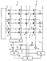
- a circuit arrangement according to the invention is shown in the figure. It contains a counting memory 1, which is divided into memory sections with different values, a memory section corresponding to a memory cell row shown. Each memory cell contains an n-channel transistor with floating gate 3 and an n-channel selection transistor 4, which are connected as indicated above. A memory cell is addressed line-wise via an address decoder 5 and column-wise via a column decoder 6. A memory cell of a control memory 2 is assigned to each row. The selection transistor of a memory cell of the control memory is driven by the same selection line 17 as the assigned row of the memory 1. Each memory cell of the control memory 2 contains an n-channel transistor 7 with a floating gate and a selection transistor 8, which are connected as indicated above.
- control gate connections of the transistors 3 of one row of the memory 1 are each connected via a transfer transistor 9 of the depletion type to the gate connection of the memory cell of the next higher value of the control memory 2.
- this control gate connection is connected to a line 11 via a further transfer transistor 10 of the depletion type.
- the gate connection of the transistor 10 is connected to the selection line 12 of this higher-order memory line.
- the circuit arrangement contains the following further logic circuits for control: a decoding device 12, with which the output read signals of a read line of the memory 1 and the read line of the memory 2, which are amplified via the sense amplifiers 13, 14, are processed; a setting device 15, by means of which the corresponding read and programming voltages for the control gates of the memory cells are provided on line 11 in the correct time; a write / erase sequence controller 16, by which the programming voltages are provided via programming amplifiers 18, 19 for the data lines of the memories 1, 2 and the setting device 15 and the transfer transistors 9 are controlled.
- the device 15 is supplied by corresponding control signals from the decoder device 12 and the sequence controller 16.
- the erase voltage provided on line 11 via device 15 is fed via transfer transistors 10, 9 to the corresponding control gate connections, the transistor 10 can be controlled accordingly by the address line 25 and the transistor 9 by the device 16. If only the control bit is deleted, the transistor 10 is activated, the transistor 9 is blocked. Writing operations are suppressed by the decoder device 12 when an incompletely written memory cell is recognized by switching off the programming amplifiers 18 and 19.
- the following voltages are set on the line 11 by the device 15: during the reading process before a writing phase, a higher reading voltage than when reading before the erasing process, in the first reading process preferably a reading voltage above the mean reading voltage, in the latter reading process an underlying reading voltage.
- a reading voltage below the high reading voltage preferably the mean reading voltage, is used.
- the erasing voltage of 20 volts is generated on line 11, for writing the voltage is 0 volts.
- the table below shows the operating cases to be decided by the decoder device 12, from which corresponding control signals are to be generated on the output lines 20, 21 of the device 12, so that the corresponding operating modes given in the table result.
- the carry bit of a counter stage of memory 1, which is available on line 22, and the assigned control bit, which is available on line 23, are evaluated as input variables.
Landscapes
- Engineering & Computer Science (AREA)
- General Physics & Mathematics (AREA)
- Computer Security & Cryptography (AREA)
- Physics & Mathematics (AREA)
- Computer Hardware Design (AREA)
- Theoretical Computer Science (AREA)
- Microelectronics & Electronic Packaging (AREA)
- General Engineering & Computer Science (AREA)
- Business, Economics & Management (AREA)
- Strategic Management (AREA)
- General Business, Economics & Management (AREA)
- Accounting & Taxation (AREA)
- Computer Networks & Wireless Communication (AREA)
- Read Only Memory (AREA)
- Credit Cards Or The Like (AREA)
- Control Of Vending Devices And Auxiliary Devices For Vending Devices (AREA)
- Meter Arrangements (AREA)
- Storage Device Security (AREA)
Applications Claiming Priority (2)
| Application Number | Priority Date | Filing Date | Title |
|---|---|---|---|
| DE4315542 | 1993-05-10 | ||
| DE4315542 | 1993-05-10 |
Publications (2)
| Publication Number | Publication Date |
|---|---|
| EP0624880A1 true EP0624880A1 (fr) | 1994-11-17 |
| EP0624880B1 EP0624880B1 (fr) | 1998-09-30 |
Family
ID=6487705
Family Applications (1)
| Application Number | Title | Priority Date | Filing Date |
|---|---|---|---|
| EP94106764A Expired - Lifetime EP0624880B1 (fr) | 1993-05-10 | 1994-04-29 | Procédé et circuit pour décompter une carte de débit |
Country Status (6)
| Country | Link |
|---|---|
| US (1) | US5511023A (fr) |
| EP (1) | EP0624880B1 (fr) |
| AT (1) | ATE171798T1 (fr) |
| DE (1) | DE59406992D1 (fr) |
| DK (1) | DK0624880T3 (fr) |
| ES (1) | ES2122075T3 (fr) |
Families Citing this family (7)
| Publication number | Priority date | Publication date | Assignee | Title |
|---|---|---|---|---|
| DE19536548A1 (de) * | 1995-09-29 | 1997-04-03 | Ibm | Vorrichtung und Verfahren zur vereinfachten Erzeugung von Werkzeugen zur Initialisierung und Personalisierung von und zur Kommunikation mit einer Chipkarte |
| US5768208A (en) * | 1996-06-18 | 1998-06-16 | Microchip Technology Incorporated | Fail safe non-volatile memory programming system and method therefor |
| GB9925227D0 (en) | 1999-10-25 | 1999-12-22 | Internet Limited | Data storage retrieval and access system |
| WO2002001521A1 (fr) * | 2000-06-28 | 2002-01-03 | G. Holdings Ltd. | Système de transaction avec dispositif personnel portatif d'identification et de contrôle de transaction |
| EP1371036A2 (fr) * | 2001-03-16 | 2003-12-17 | G. Holdings Ltd | Systeme et methode de renouvellement de donnees d'identification sur un dispositif de transaction portatif |
| US8626642B2 (en) | 2003-08-22 | 2014-01-07 | Compucredit Intellectual Property Holdings Corp. Iii | System and method for dynamically managing a financial account |
| US7204412B2 (en) * | 2003-10-14 | 2007-04-17 | Compucredit Intellectual Property Holdings Corp. Iii | Family stored value card program |
Citations (6)
| Publication number | Priority date | Publication date | Assignee | Title |
|---|---|---|---|---|
| US4301535A (en) * | 1979-07-02 | 1981-11-17 | Mostek Corporation | Programmable read only memory integrated circuit with bit-check and deprogramming modes and methods for programming and testing said circuit |
| JPS5936393A (ja) * | 1982-08-20 | 1984-02-28 | Mitsubishi Electric Corp | 不揮発性半導体メモリ装置 |
| WO1986006205A1 (fr) * | 1985-04-12 | 1986-10-23 | Eurotechnique | Memoire morte programmable electriquement |
| EP0321727A1 (fr) * | 1987-12-17 | 1989-06-28 | Siemens Aktiengesellschaft | Méthode et circuit de protection contre la manipulation de dévalorisation de mémoires EEPROM |
| GB2214379A (en) * | 1988-01-12 | 1989-08-31 | Intel Corp | Voltage margining circuit for flash eprom |
| EP0519847A1 (fr) * | 1991-06-20 | 1992-12-23 | France Telecom | Carte à mémoire de comptage de données et appareil de lecture |
Family Cites Families (3)
| Publication number | Priority date | Publication date | Assignee | Title |
|---|---|---|---|---|
| DK174975B1 (da) * | 1988-05-06 | 2004-04-05 | Toppan Printing Co Ltd | Integreret kredsløbskort |
| FR2686998B1 (fr) * | 1992-01-30 | 1994-03-25 | Gemplus Card International | Carte a puce a plusieurs protocoles de communication. |
| JPH05233901A (ja) * | 1992-02-18 | 1993-09-10 | Mitsubishi Electric Corp | Icカード、icカード搭載用メモリic及びicカードのメモリ容量の確認方法 |
-
1994
- 1994-04-29 ES ES94106764T patent/ES2122075T3/es not_active Expired - Lifetime
- 1994-04-29 EP EP94106764A patent/EP0624880B1/fr not_active Expired - Lifetime
- 1994-04-29 DE DE59406992T patent/DE59406992D1/de not_active Expired - Lifetime
- 1994-04-29 DK DK94106764T patent/DK0624880T3/da active
- 1994-04-29 AT AT94106764T patent/ATE171798T1/de active
- 1994-05-10 US US08/240,928 patent/US5511023A/en not_active Expired - Lifetime
Patent Citations (6)
| Publication number | Priority date | Publication date | Assignee | Title |
|---|---|---|---|---|
| US4301535A (en) * | 1979-07-02 | 1981-11-17 | Mostek Corporation | Programmable read only memory integrated circuit with bit-check and deprogramming modes and methods for programming and testing said circuit |
| JPS5936393A (ja) * | 1982-08-20 | 1984-02-28 | Mitsubishi Electric Corp | 不揮発性半導体メモリ装置 |
| WO1986006205A1 (fr) * | 1985-04-12 | 1986-10-23 | Eurotechnique | Memoire morte programmable electriquement |
| EP0321727A1 (fr) * | 1987-12-17 | 1989-06-28 | Siemens Aktiengesellschaft | Méthode et circuit de protection contre la manipulation de dévalorisation de mémoires EEPROM |
| GB2214379A (en) * | 1988-01-12 | 1989-08-31 | Intel Corp | Voltage margining circuit for flash eprom |
| EP0519847A1 (fr) * | 1991-06-20 | 1992-12-23 | France Telecom | Carte à mémoire de comptage de données et appareil de lecture |
Non-Patent Citations (1)
| Title |
|---|
| PATENT ABSTRACTS OF JAPAN vol. 8, no. 137 (P - 282) 26 June 1984 (1984-06-26) * |
Also Published As
| Publication number | Publication date |
|---|---|
| DE59406992D1 (de) | 1998-11-05 |
| DK0624880T3 (da) | 1999-06-21 |
| ATE171798T1 (de) | 1998-10-15 |
| US5511023A (en) | 1996-04-23 |
| EP0624880B1 (fr) | 1998-09-30 |
| ES2122075T3 (es) | 1998-12-16 |
Similar Documents
| Publication | Publication Date | Title |
|---|---|---|
| DE69620504T2 (de) | Apparat und verfahren zur verwendung von identifikationsmarken für radiofrequenzen | |
| DE4207934C2 (de) | Nichtflüchtige Halbleiterspeichervorrichtung und Programmierverfahren für eine nichtflüchtige Halbleiterspeichervorrichtung | |
| DE2621271C2 (de) | Tragbarer Datenträger | |
| DE2837201C2 (fr) | ||
| EP0195885B1 (fr) | Procédé et dispositif pour l'emmagasinage non volatil de l'état du compte d'un circuit de comptage électronique | |
| DE69615736T2 (de) | Speicherkarte und Vorrichtung zum Betrieb einer solchen Karte | |
| EP0129054A1 (fr) | Circuit comprenant une mémoire de données et une mémoire de commande pour la lecture, l'écriture et l'effacement de la mémoire de données | |
| DE69401291T2 (de) | Integrierte Schaltung für Speicherkarte und Verfahren zum Abzählen der Einheiten in einer Speicherkarte | |
| DE3243935C2 (fr) | ||
| EP0321727A1 (fr) | Méthode et circuit de protection contre la manipulation de dévalorisation de mémoires EEPROM | |
| WO2005104134A1 (fr) | Procede et dispositif de programmation de cellules de memoire cbram | |
| EP0624880B1 (fr) | Procédé et circuit pour décompter une carte de débit | |
| DE69602984T2 (de) | Verfahren zum Schützen nichtflüchtiger Speicherbereiche | |
| DE69218053T2 (de) | Speicherkarte zur Zählung von Daten und Lesevorrichtung | |
| DE69700379T2 (de) | Elektrisch modifizierbarer nichtflüchtiger Mehrpegelspeicher mit internen Auffrischungsmitteln | |
| EP0123177B1 (fr) | Méthode et appareil pour commander une mémoire non volatile écriture/lecture d'utilisation | |
| DE69508207T2 (de) | Speicherwörterzugangsschutzvorrichtung | |
| DE69101099T2 (de) | Verfahren zum Bestätigen geheimer Kodes in Speicherkarten. | |
| DE3784664T2 (de) | Schutzvorrichtung fuer einen loesch- und neuprogrammierbaren festwertspeicher. | |
| EP0086360B1 (fr) | Mémoire non-volatile programmable électriquement par mot et utilisation d'une telle mémoire | |
| EP0070461B1 (fr) | Compteur à mémoire non volatile | |
| EP1040487B1 (fr) | Procede pour la modification securisee d'une valeur memorisee dans une memoire remanente et circuit a cet effet | |
| EP0663667B1 (fr) | Circuit intégré de mémoire à semi-conducteurs, et méthode d'opération | |
| DE102006040571B4 (de) | Vorrichtung und Verfahren zum Auslesen einer Speicherinformation | |
| EP1163679B1 (fr) | Procede permettant de faire fonctionner une memoire integree a cellules inscriptibles et memoire integree associee |
Legal Events
| Date | Code | Title | Description |
|---|---|---|---|
| PUAI | Public reference made under article 153(3) epc to a published international application that has entered the european phase |
Free format text: ORIGINAL CODE: 0009012 |
|
| AK | Designated contracting states |
Kind code of ref document: A1 Designated state(s): AT BE CH DE DK ES FR GB GR IE IT LI NL PT SE |
|
| 17P | Request for examination filed |
Effective date: 19941205 |
|
| GRAG | Despatch of communication of intention to grant |
Free format text: ORIGINAL CODE: EPIDOS AGRA |
|
| 17Q | First examination report despatched |
Effective date: 19970919 |
|
| GRAG | Despatch of communication of intention to grant |
Free format text: ORIGINAL CODE: EPIDOS AGRA |
|
| GRAG | Despatch of communication of intention to grant |
Free format text: ORIGINAL CODE: EPIDOS AGRA |
|
| GRAH | Despatch of communication of intention to grant a patent |
Free format text: ORIGINAL CODE: EPIDOS IGRA |
|
| GRAH | Despatch of communication of intention to grant a patent |
Free format text: ORIGINAL CODE: EPIDOS IGRA |
|
| GRAA | (expected) grant |
Free format text: ORIGINAL CODE: 0009210 |
|
| AK | Designated contracting states |
Kind code of ref document: B1 Designated state(s): AT BE CH DE DK ES FR GB GR IE IT LI NL PT SE |
|
| REF | Corresponds to: |
Ref document number: 171798 Country of ref document: AT Date of ref document: 19981015 Kind code of ref document: T |
|
| REG | Reference to a national code |
Ref country code: CH Ref legal event code: NV Representative=s name: SIEMENS SCHWEIZ AG Ref country code: CH Ref legal event code: EP |
|
| REF | Corresponds to: |
Ref document number: 59406992 Country of ref document: DE Date of ref document: 19981105 |
|
| REG | Reference to a national code |
Ref country code: IE Ref legal event code: FG4D Free format text: GERMAN Ref country code: ES Ref legal event code: FG2A Ref document number: 2122075 Country of ref document: ES Kind code of ref document: T3 |
|
| ET | Fr: translation filed | ||
| GBT | Gb: translation of ep patent filed (gb section 77(6)(a)/1977) |
Effective date: 19981201 |
|
| REG | Reference to a national code |
Ref country code: PT Ref legal event code: SC4A Free format text: AVAILABILITY OF NATIONAL TRANSLATION Effective date: 19981211 |
|
| REG | Reference to a national code |
Ref country code: DK Ref legal event code: T3 |
|
| PLBE | No opposition filed within time limit |
Free format text: ORIGINAL CODE: 0009261 |
|
| STAA | Information on the status of an ep patent application or granted ep patent |
Free format text: STATUS: NO OPPOSITION FILED WITHIN TIME LIMIT |
|
| 26N | No opposition filed | ||
| REG | Reference to a national code |
Ref country code: GB Ref legal event code: IF02 |
|
| PGFP | Annual fee paid to national office [announced via postgrant information from national office to epo] |
Ref country code: PT Payment date: 20040318 Year of fee payment: 11 |
|
| PGFP | Annual fee paid to national office [announced via postgrant information from national office to epo] |
Ref country code: IE Payment date: 20040324 Year of fee payment: 11 |
|
| PGFP | Annual fee paid to national office [announced via postgrant information from national office to epo] |
Ref country code: GR Payment date: 20040326 Year of fee payment: 11 |
|
| PGFP | Annual fee paid to national office [announced via postgrant information from national office to epo] |
Ref country code: NL Payment date: 20040331 Year of fee payment: 11 |
|
| PGFP | Annual fee paid to national office [announced via postgrant information from national office to epo] |
Ref country code: SE Payment date: 20040402 Year of fee payment: 11 |
|
| PGFP | Annual fee paid to national office [announced via postgrant information from national office to epo] |
Ref country code: DK Payment date: 20040405 Year of fee payment: 11 |
|
| PGFP | Annual fee paid to national office [announced via postgrant information from national office to epo] |
Ref country code: BE Payment date: 20040527 Year of fee payment: 11 |
|
| PG25 | Lapsed in a contracting state [announced via postgrant information from national office to epo] |
Ref country code: IE Free format text: LAPSE BECAUSE OF NON-PAYMENT OF DUE FEES Effective date: 20050429 |
|
| PG25 | Lapsed in a contracting state [announced via postgrant information from national office to epo] |
Ref country code: SE Free format text: LAPSE BECAUSE OF NON-PAYMENT OF DUE FEES Effective date: 20050430 Ref country code: BE Free format text: LAPSE BECAUSE OF NON-PAYMENT OF DUE FEES Effective date: 20050430 |
|
| PG25 | Lapsed in a contracting state [announced via postgrant information from national office to epo] |
Ref country code: DK Free format text: LAPSE BECAUSE OF NON-PAYMENT OF DUE FEES Effective date: 20050502 |
|
| BERE | Be: lapsed |
Owner name: *SIEMENS A.G. Effective date: 20050430 |
|
| PG25 | Lapsed in a contracting state [announced via postgrant information from national office to epo] |
Ref country code: PT Free format text: LAPSE BECAUSE OF NON-PAYMENT OF DUE FEES Effective date: 20051031 |
|
| PG25 | Lapsed in a contracting state [announced via postgrant information from national office to epo] |
Ref country code: NL Free format text: LAPSE BECAUSE OF NON-PAYMENT OF DUE FEES Effective date: 20051101 |
|
| PG25 | Lapsed in a contracting state [announced via postgrant information from national office to epo] |
Ref country code: GR Free format text: LAPSE BECAUSE OF NON-PAYMENT OF DUE FEES Effective date: 20051103 |
|
| REG | Reference to a national code |
Ref country code: DK Ref legal event code: EBP |
|
| EUG | Se: european patent has lapsed | ||
| NLV4 | Nl: lapsed or anulled due to non-payment of the annual fee |
Effective date: 20051101 |
|
| BERE | Be: lapsed |
Owner name: *SIEMENS A.G. Effective date: 20050430 |
|
| REG | Reference to a national code |
Ref country code: CH Ref legal event code: PCAR Free format text: SIEMENS SCHWEIZ AG;INTELLECTUAL PROPERTY FREILAGERSTRASSE 40;8047 ZUERICH (CH) |
|
| REG | Reference to a national code |
Ref country code: CH Ref legal event code: PUE Owner name: INFINEON TECHNOLOGIES AG Free format text: SIEMENS AKTIENGESELLSCHAFT#WITTELSBACHERPLATZ 2#80333 MUENCHEN (DE) -TRANSFER TO- INFINEON TECHNOLOGIES AG#AM CAMPEON 1-12#85579 NEUBIBERG (DE) |
|
| REG | Reference to a national code |
Ref country code: GB Ref legal event code: 732E Free format text: REGISTERED BETWEEN 20110707 AND 20110713 |
|
| REG | Reference to a national code |
Ref country code: FR Ref legal event code: TP Owner name: INFINEON TECHNOLOGIES AG, DE Effective date: 20110922 |
|
| REG | Reference to a national code |
Ref country code: ES Ref legal event code: PC2A Owner name: INFINEON TECHNOLOGIES AG Effective date: 20111103 |
|
| REG | Reference to a national code |
Ref country code: DE Ref legal event code: R081 Ref document number: 59406992 Country of ref document: DE Owner name: INFINEON TECHNOLOGIES AG, DE Free format text: FORMER OWNER: SIEMENS AKTIENGESELLSCHAFT, 80333 MUENCHEN, DE Effective date: 20111107 |
|
| REG | Reference to a national code |
Ref country code: AT Ref legal event code: PC Ref document number: 171798 Country of ref document: AT Kind code of ref document: T Owner name: INFINEON TECHNOLOGIES AG, DE Effective date: 20120419 |
|
| PGFP | Annual fee paid to national office [announced via postgrant information from national office to epo] |
Ref country code: ES Payment date: 20120425 Year of fee payment: 19 |
|
| PGFP | Annual fee paid to national office [announced via postgrant information from national office to epo] |
Ref country code: AT Payment date: 20120411 Year of fee payment: 19 |
|
| PGFP | Annual fee paid to national office [announced via postgrant information from national office to epo] |
Ref country code: DE Payment date: 20130613 Year of fee payment: 20 Ref country code: CH Payment date: 20130422 Year of fee payment: 20 Ref country code: GB Payment date: 20130418 Year of fee payment: 20 |
|
| PGFP | Annual fee paid to national office [announced via postgrant information from national office to epo] |
Ref country code: IT Payment date: 20130424 Year of fee payment: 20 Ref country code: FR Payment date: 20130515 Year of fee payment: 20 |
|
| REG | Reference to a national code |
Ref country code: DE Ref legal event code: R071 Ref document number: 59406992 Country of ref document: DE |
|
| REG | Reference to a national code |
Ref country code: CH Ref legal event code: PL |
|
| REG | Reference to a national code |
Ref country code: GB Ref legal event code: PE20 Expiry date: 20140428 |
|
| REG | Reference to a national code |
Ref country code: AT Ref legal event code: MK07 Ref document number: 171798 Country of ref document: AT Kind code of ref document: T Effective date: 20140429 |
|
| PG25 | Lapsed in a contracting state [announced via postgrant information from national office to epo] |
Ref country code: GB Free format text: LAPSE BECAUSE OF EXPIRATION OF PROTECTION Effective date: 20140428 |
|
| PG25 | Lapsed in a contracting state [announced via postgrant information from national office to epo] |
Ref country code: DE Free format text: LAPSE BECAUSE OF EXPIRATION OF PROTECTION Effective date: 20140430 |
|
| REG | Reference to a national code |
Ref country code: ES Ref legal event code: FD2A Effective date: 20140926 |
|
| PG25 | Lapsed in a contracting state [announced via postgrant information from national office to epo] |
Ref country code: ES Free format text: LAPSE BECAUSE OF EXPIRATION OF PROTECTION Effective date: 20140430 |