EP0663667B1 - Circuit intégré de mémoire à semi-conducteurs, et méthode d'opération - Google Patents
Circuit intégré de mémoire à semi-conducteurs, et méthode d'opération Download PDFInfo
- Publication number
- EP0663667B1 EP0663667B1 EP94120451A EP94120451A EP0663667B1 EP 0663667 B1 EP0663667 B1 EP 0663667B1 EP 94120451 A EP94120451 A EP 94120451A EP 94120451 A EP94120451 A EP 94120451A EP 0663667 B1 EP0663667 B1 EP 0663667B1
- Authority
- EP
- European Patent Office
- Prior art keywords
- potential
- blh
- bit line
- semiconductor memory
- bit lines
- Prior art date
- Legal status (The legal status is an assumption and is not a legal conclusion. Google has not performed a legal analysis and makes no representation as to the accuracy of the status listed.)
- Expired - Lifetime
Links
- 239000004065 semiconductor Substances 0.000 title claims abstract description 20
- 239000003990 capacitor Substances 0.000 claims abstract description 21
- 238000000034 method Methods 0.000 claims description 4
- 239000011159 matrix material Substances 0.000 claims 1
- 238000011161 development Methods 0.000 description 2
- 230000018109 developmental process Effects 0.000 description 2
- 238000011156 evaluation Methods 0.000 description 2
- 230000007423 decrease Effects 0.000 description 1
- 230000006870 function Effects 0.000 description 1
- 238000011017 operating method Methods 0.000 description 1
- 230000002787 reinforcement Effects 0.000 description 1
Images
Classifications
-
- G—PHYSICS
- G11—INFORMATION STORAGE
- G11C—STATIC STORES
- G11C11/00—Digital stores characterised by the use of particular electric or magnetic storage elements; Storage elements therefor
- G11C11/21—Digital stores characterised by the use of particular electric or magnetic storage elements; Storage elements therefor using electric elements
- G11C11/34—Digital stores characterised by the use of particular electric or magnetic storage elements; Storage elements therefor using electric elements using semiconductor devices
- G11C11/40—Digital stores characterised by the use of particular electric or magnetic storage elements; Storage elements therefor using electric elements using semiconductor devices using transistors
- G11C11/401—Digital stores characterised by the use of particular electric or magnetic storage elements; Storage elements therefor using electric elements using semiconductor devices using transistors forming cells needing refreshing or charge regeneration, i.e. dynamic cells
- G11C11/4063—Auxiliary circuits, e.g. for addressing, decoding, driving, writing, sensing or timing
- G11C11/407—Auxiliary circuits, e.g. for addressing, decoding, driving, writing, sensing or timing for memory cells of the field-effect type
-
- G—PHYSICS
- G11—INFORMATION STORAGE
- G11C—STATIC STORES
- G11C11/00—Digital stores characterised by the use of particular electric or magnetic storage elements; Storage elements therefor
- G11C11/21—Digital stores characterised by the use of particular electric or magnetic storage elements; Storage elements therefor using electric elements
- G11C11/34—Digital stores characterised by the use of particular electric or magnetic storage elements; Storage elements therefor using electric elements using semiconductor devices
- G11C11/40—Digital stores characterised by the use of particular electric or magnetic storage elements; Storage elements therefor using electric elements using semiconductor devices using transistors
- G11C11/401—Digital stores characterised by the use of particular electric or magnetic storage elements; Storage elements therefor using electric elements using semiconductor devices using transistors forming cells needing refreshing or charge regeneration, i.e. dynamic cells
- G11C11/4063—Auxiliary circuits, e.g. for addressing, decoding, driving, writing, sensing or timing
- G11C11/407—Auxiliary circuits, e.g. for addressing, decoding, driving, writing, sensing or timing for memory cells of the field-effect type
- G11C11/409—Read-write [R-W] circuits
- G11C11/4099—Dummy cell treatment; Reference voltage generators
Definitions
- the invention relates to an integrated semiconductor memory circuit with the features of the preamble according to claim 1 and a method for operating the same.
- a semiconductor memory circuit is known for example from EP-A-0 398 245.
- bit lines BL precharged to a bit line potential VBL (generally as a pre-charge process or with pre-charge potential designated).
- VBL bit line potential
- SA the sense amplifiers SA (which yes in the general flip-flop circuits that are differential work) after reading for evaluation and reinforcement of the Read signals effectively feed these only because of the bitline potential VBL at both inputs of the sense amplifier SA with the same value and therefore different from the working sense amplifiers SA is not taken into account.
- Dummy cells are also commonly used these are charged to the bit line potential VBL.
- Integrated semiconductor memory circuits are known in particular of the transistor memory cell type (so-called 1T DRAMs or embedded 1T-DRAM's), sensitive to so-called Soft errors, i.e. against alpha rays, the most derive from the block housing used.
- 1T DRAMs or embedded 1T-DRAM's transistor memory cell type
- Soft errors i.e. against alpha rays
- the object of the present invention is to generic integrated To optimize semiconductor memory circuits so that their sense amplifiers the data phys. 0 and phys. 1 with approximately can recognize the same security (so-called symmetrization of the Sense amplifier with respect to phys. 0 and phys. 1), without the Having to enlarge memory cells and without sacrificing anything to have to accept security against soft errors. It is also the task to develop an appropriate operating procedure for to specify such a semiconductor memory circuit.
- the present invention enables the soft error rate to be changed lower two orders of magnitude compared to the known, Generic semiconductor memory circuits.
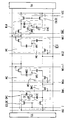
- a bit line BL is shown with its two bit line halves BLH, BLH , to which on one side a sense amplifier SA is connected and on the other side a precharging device EQL for precharging and (with regard to its electrical potential) equating the bit line halves BLH, BLH to a bit line potential VBL before reading data from memory cells MC.
- memory cells MC of the transistor type are shown (with selection transistors MCT and storage capacitors MCC), on the one hand with the respective bit line half BLH, BLH are connected and on the other hand (on the first electrodes of their storage capacitors MCC) all together with a so-called plate potential VPL.
- This has essentially half the value of the difference between the supply voltage potential VDD (or internal supply voltage potential VDDint) and the reference potential VSS. It is therefore essentially equal to the bit line potential VBL, which can be applied to the bit lines BL via the precharging device EQL.
- the plate potential VPL could also essentially have the value of the supply voltage potential VDD (or that of the internal supply voltage potential VDDint) or the reference potential VSS.
- the figure shows word lines WL (numbered from WL1 to WLn) for driving the selection transistors MCT of the memory cells MC.
- the memory cells MC are thus, as is generally customary, arranged at intersections between word lines WL and bit lines BL and, via their selection transistors MCT, for reading and storing information with the respective bit lines BL or bit line halves BLH; BLH connectable.
- Each bit line half BLH, BLH has (for example, arranged at its ends as shown) a so-called dummy cell DMC, which is also of the transistor cell type. As is generally known, this serves to uniformly and symmetrically load the differentially operating sense amplifiers SA during operation.
- the storage capacitors DC of the dummy cells DMC are also connected to the plate potential VPL at their first electrodes.
- marginal cells CMC which are generally referred to as "friendly cells” are called, but they will only be later as they are not described for the present invention are absolutely necessary.
- the previously described semiconductor memory circuit corresponds fully state of the art. According to the invention, this semiconductor memory circuit however, additional devices EQLDC, by means of which the second electrodes of the Storage capacitors DC of the dummy memory cells DMC in operation can be charged with a precharge potential VDC.
- the loading takes place according to the invention during (usual) precharging of the bit lines BL to the bit line potential VBL.
- the value of the precharge potential VDC is 5 to 35% greater than the value of half the difference from the supply voltage potential VDD (or VDDint when using an internal Supply voltage potential) and reference potential VSS.
- the devices EQLDC can, for example, as shown, Transistors contain the one with the precharge potential VDC are connected and on the other hand to the second electrodes of the storage capacitors DC of the dummy cells DMC.
- the transistors are gated by a precharge clock signal T, which at the time of precharging the transistors switch.
- the precharge clock signal T can be the same in time Have a course like a corresponding one (not shown) Clock signal, which is read out of data from the memory cells MC precharging the bit lines BL to their bit line potential VBL controls.
- marginal cells CMC which are generally referred to as "friendly cells” be designated. Their function is known to the expert. she can either consist only of edge cell capacitors CC, as shown here. But you can also go beyond still contain transistors, similar to the selection transistors MCT of memory cells MC or of dummy cells DMC.
- first electrodes of the edge cell capacitors CC with the plate potential VPL connected and the second electrodes of this Edge cell capacitors CC are by means of the equalizers EQLDC for the dummy cells DMC also with the precharge potential VDC of the DMC dummy cells can be applied. This then results in an even better symmetry of the working and Load ratios of the sense amplifier SA when reading out as well as evaluating and amplifying the data read out.
Landscapes
- Engineering & Computer Science (AREA)
- Microelectronics & Electronic Packaging (AREA)
- Computer Hardware Design (AREA)
- Dram (AREA)
- Credit Cards Or The Like (AREA)
Claims (4)
- Circuit intégré de mémoire à semi-conducteurscaractérisé en ce que le potentiel de précharge a une valeur qui est 5 à 35 % plus grande que la valeur de la moitié de la différence entre le potentiel de tension d'alimentation et le potentiel de référence.comportant un potentiel de tension d'alimentation et comportant un potentiel de référence,comportant des cellules (MC) de mémoire du type à un transistor, qui contiennent chacune un transistor de sélection et au moins un condensateur (MCC) d'accumulation et qui sont disposées de manière matricielle aux points d'intersection de lignes (WL ; WL1 ... Wln) de transmission de mots et de lignes (BL) de transmission de bits,chaque ligne (BL) de transmission de bits étant formée par deux moitiés (BLH,
BLH ) de lignes de transmission de bits, et étant chargée au cours du fonctionnement à la moitié de la différence entre le potentiel d'alimentation et le potentiel de référence, etchaque cellule (MC) de mémoire étant d'une part reliée à une moitié (BLH ;BLH ) de lignes de transmission de bits associées par l'intermédiaire de son transistor de sélection et, d'autre part, une première électrode de l'au moins un condensateur (MCC) d'accumulation étant reliée au cours du fonctionnement à un potentiel (VPL) de plaque d'une valeur prescrite,comportant au moins une cellule (DMC) de mémoire Dummy, contenant également au moins un condensateur (DC) d'accumulation, pour chaque moitié (BLH ;BLH ) de ligne de transmission de bits, également une première électrode de l'au moins un condensateur (DC) d'accumulation étant également reliée au cours du fonctionnement au potentiel (VPL) de plaque,comportant des dispositifs (EQLDC) au moyen desquels les deuxièmes électrodes des condensateurs (DC) d'accumulation des cellules (DMC) de mémoire Dummy peuvent être mises au cours du fonctionnement à un potentiel (VDC) de précharge, - Circuit intégré de mémoire à semi-conducteurs suivant la revendication 1, comportant au moins une cellule (CMC) de bord pour chaque moitié (BLH ;
BLH ) de lignes de transmission de bits, qui contient au moins un condensateur (CC) de cellule de bord dont la première électrode est reliée au potentiel (VPL) de plaque, caractérisé en ce que la deuxième électrode du condensateur (CC) de cellules de bord peut être mise au potentiel (VDC) de précharge. - Procédé pour faire fonctionner un circuit intégré de mémoire à semi-conducteurs comportant les caractéristiques des revendications 1 ou 2, dans lequel, avant de lire des données enregistrées dans des cellules (MC) de mémoire, on précharge les lignes (BL) de transmission de bits à un potentiel (VBL) de lignes de transmission de bits, le potentiel (VDC) de précharge étant, lors de la précharge des lignes (BL) de transmission de bits, appliqué aux deuxièmes électrodes des condensateurs (DC) d'accumulation des cellules (DMC) de mémoire Dummy.
- Procédé suivant la revendication 3, le potentiel (VDC) de précharge étant, lors de la précharge des lignes (BL) de transmission de bits, appliqué aussi aux deuxièmes électrodes des condensateurs (CC) de cellules de bord.
Applications Claiming Priority (2)
| Application Number | Priority Date | Filing Date | Title |
|---|---|---|---|
| DE4400699 | 1994-01-12 | ||
| DE4400699 | 1994-01-12 |
Publications (3)
| Publication Number | Publication Date |
|---|---|
| EP0663667A2 EP0663667A2 (fr) | 1995-07-19 |
| EP0663667A3 EP0663667A3 (fr) | 1995-10-25 |
| EP0663667B1 true EP0663667B1 (fr) | 1999-03-03 |
Family
ID=6507778
Family Applications (1)
| Application Number | Title | Priority Date | Filing Date |
|---|---|---|---|
| EP94120451A Expired - Lifetime EP0663667B1 (fr) | 1994-01-12 | 1994-12-22 | Circuit intégré de mémoire à semi-conducteurs, et méthode d'opération |
Country Status (6)
| Country | Link |
|---|---|
| US (1) | US5574694A (fr) |
| EP (1) | EP0663667B1 (fr) |
| JP (1) | JP3857330B2 (fr) |
| KR (1) | KR100383291B1 (fr) |
| AT (1) | ATE177246T1 (fr) |
| DE (1) | DE59407879D1 (fr) |
Families Citing this family (6)
| Publication number | Priority date | Publication date | Assignee | Title |
|---|---|---|---|---|
| DE19503782A1 (de) * | 1995-02-04 | 1996-08-08 | Philips Patentverwaltung | Verzögerungsschaltung |
| JP3824370B2 (ja) * | 1997-03-03 | 2006-09-20 | 富士通株式会社 | 半導体装置 |
| JP4084149B2 (ja) * | 2002-09-13 | 2008-04-30 | 富士通株式会社 | 半導体記憶装置 |
| KR100908699B1 (ko) * | 2002-09-13 | 2009-07-22 | 주식회사 포스코 | 폐수처리설비 오일분리조의 부유물 제거장치 |
| JP5700907B2 (ja) * | 2008-06-26 | 2015-04-15 | ピーエスフォー ルクスコ エスエイアールエルPS4 Luxco S.a.r.l. | 半導体記憶装置 |
| US20100269845A1 (en) * | 2009-04-23 | 2010-10-28 | Bernhard Peter Tamme | Hair styling device & methods of use thereof |
Family Cites Families (10)
| Publication number | Priority date | Publication date | Assignee | Title |
|---|---|---|---|---|
| GB1523752A (en) * | 1974-08-28 | 1978-09-06 | Siemens Ag | Dynamic semiconductor data stores |
| US4658382A (en) * | 1984-07-11 | 1987-04-14 | Texas Instruments Incorporated | Dynamic memory with improved dummy cell circuitry |
| US4598389A (en) * | 1984-10-01 | 1986-07-01 | Texas Instruments Incorporated | Single-ended CMOS sense amplifier |
| JPS6282597A (ja) * | 1985-10-08 | 1987-04-16 | Fujitsu Ltd | 半導体記憶装置 |
| US5255235A (en) * | 1987-05-15 | 1993-10-19 | Mitsubishi Denki Kabushiki Kaisha | Dynamic random access memory with dummy word lines connected to bit line potential adjusting capacitors |
| JPS63282993A (ja) * | 1987-05-15 | 1988-11-18 | Mitsubishi Electric Corp | 半導体ダイナミック・ランダム・アクセス・メモリ |
| JPH01119984A (ja) * | 1987-10-31 | 1989-05-12 | Toshiba Corp | ダイナミック型半導体メモリ |
| JPH0762955B2 (ja) * | 1989-05-15 | 1995-07-05 | 株式会社東芝 | ダイナミック型ランダムアクセスメモリ |
| US5301157A (en) * | 1992-06-01 | 1994-04-05 | Micron Technology, Inc. | Coupling circuit and method for discharging a non-selected bit line during accessing of a memory storage cell |
| US5291437A (en) * | 1992-06-25 | 1994-03-01 | Texas Instruments Incorporated | Shared dummy cell |
-
1994
- 1994-12-22 EP EP94120451A patent/EP0663667B1/fr not_active Expired - Lifetime
- 1994-12-22 AT AT94120451T patent/ATE177246T1/de not_active IP Right Cessation
- 1994-12-22 DE DE59407879T patent/DE59407879D1/de not_active Expired - Fee Related
-
1995
- 1995-01-05 KR KR1019950000072A patent/KR100383291B1/ko not_active Expired - Fee Related
- 1995-01-09 JP JP01749695A patent/JP3857330B2/ja not_active Expired - Fee Related
- 1995-01-12 US US08/371,827 patent/US5574694A/en not_active Expired - Fee Related
Also Published As
| Publication number | Publication date |
|---|---|
| EP0663667A2 (fr) | 1995-07-19 |
| DE59407879D1 (de) | 1999-04-08 |
| JP3857330B2 (ja) | 2006-12-13 |
| ATE177246T1 (de) | 1999-03-15 |
| EP0663667A3 (fr) | 1995-10-25 |
| JPH07235179A (ja) | 1995-09-05 |
| US5574694A (en) | 1996-11-12 |
| KR950033216A (ko) | 1995-12-22 |
| KR100383291B1 (ko) | 2003-06-25 |
| HK1004240A1 (en) | 1998-11-20 |
Similar Documents
| Publication | Publication Date | Title |
|---|---|---|
| DE69427184T2 (de) | Ein Referenzspannungsgenerator und eine dieselbe verwendende Halbleiterspeicheranordnung | |
| EP1118081B1 (fr) | Memoire integree dotee d'un amplificateur de lecture differentiel | |
| DE69620318T2 (de) | Ferroelektrische Speicheranordnungen und Verfahren zu ihrer Prüfung | |
| DE69022312T2 (de) | Halbleiterspeichergerät. | |
| DE69621293T2 (de) | Ferroelektrische Speichervorrichtung | |
| DE4003673A1 (de) | Erweiterte schnellschreibschaltung fuer den dram-test | |
| DE19756929B4 (de) | Zellenarray und Leseverstärkerstruktur mit verbesserten Rauscheigenschaften und verringerter Größe | |
| DE69127317T2 (de) | Halbleiterspeicherschaltung | |
| DE60107174T2 (de) | Halbleiterspeicheranordnung | |
| EP0991079B1 (fr) | Mémoire intégrée | |
| EP0663667B1 (fr) | Circuit intégré de mémoire à semi-conducteurs, et méthode d'opération | |
| DE10154613B4 (de) | Verfahren zum Vorladen von Speicherzellen eines dynamischen Halbleiterspeichers beim Power Up sowie Halbleiterspeicher | |
| DE69521721T2 (de) | Verbesserter halbleiterspeicher mit einem zeilenauswahlsignal ausgebendem zeilendekoders | |
| EP0663666B1 (fr) | Circuit intégré de mémoire à semi-conducteurs et méthode d'opération | |
| DE19952311B4 (de) | Integrierter Speicher mit Speicherzellen vom 2-Transistor/2-Kondensator-Typ | |
| EP1102168B1 (fr) | Mémoire intégrée avec des cellules de mémoire et des cellules de référence | |
| EP1163677B1 (fr) | Memoire integree a cellules de memoire et a cellules de reference et procede de fonctionnement de ladite memoire | |
| DE19647135A1 (de) | Halbleiterspeichervorrichtung | |
| EP1163675B1 (fr) | Memoire integree a cellules de memoire et a cellules de reference et procede de fonctionnement de ladite memoire | |
| EP0732703B1 (fr) | Procédé pour tester un circuit de mémoire à semi-conducteur | |
| DE19903198C1 (de) | Integrierter Speicher und entsprechendes Betriebsverfahren | |
| EP0967616B1 (fr) | Mémoire intégrée | |
| EP0897181B1 (fr) | Circuit de traitement de données de cellules de mémoire | |
| DE10315087B3 (de) | Verfahren zum Auffrischen von dynamischen Speicherzellen in einer Speicherschaltung und einer Speicherschaltung | |
| DE10392198T5 (de) | Erhöhen einer Auffrischperiode (Refresh Period) in einer Halbleiterspeichervorrichtung |
Legal Events
| Date | Code | Title | Description |
|---|---|---|---|
| PUAI | Public reference made under article 153(3) epc to a published international application that has entered the european phase |
Free format text: ORIGINAL CODE: 0009012 |
|
| AK | Designated contracting states |
Kind code of ref document: A2 Designated state(s): AT DE FR GB IE IT NL |
|
| PUAL | Search report despatched |
Free format text: ORIGINAL CODE: 0009013 |
|
| AK | Designated contracting states |
Kind code of ref document: A3 Designated state(s): AT DE FR GB IE IT NL |
|
| 17P | Request for examination filed |
Effective date: 19960419 |
|
| GRAG | Despatch of communication of intention to grant |
Free format text: ORIGINAL CODE: EPIDOS AGRA |
|
| GRAG | Despatch of communication of intention to grant |
Free format text: ORIGINAL CODE: EPIDOS AGRA |
|
| GRAH | Despatch of communication of intention to grant a patent |
Free format text: ORIGINAL CODE: EPIDOS IGRA |
|
| 17Q | First examination report despatched |
Effective date: 19980706 |
|
| GRAH | Despatch of communication of intention to grant a patent |
Free format text: ORIGINAL CODE: EPIDOS IGRA |
|
| GRAA | (expected) grant |
Free format text: ORIGINAL CODE: 0009210 |
|
| AK | Designated contracting states |
Kind code of ref document: B1 Designated state(s): AT DE FR GB IE IT NL |
|
| REF | Corresponds to: |
Ref document number: 177246 Country of ref document: AT Date of ref document: 19990315 Kind code of ref document: T |
|
| REG | Reference to a national code |
Ref country code: IE Ref legal event code: FG4D Free format text: GERMAN |
|
| REF | Corresponds to: |
Ref document number: 59407879 Country of ref document: DE Date of ref document: 19990408 |
|
| ET | Fr: translation filed | ||
| ITF | It: translation for a ep patent filed | ||
| GBT | Gb: translation of ep patent filed (gb section 77(6)(a)/1977) |
Effective date: 19990506 |
|
| PLBE | No opposition filed within time limit |
Free format text: ORIGINAL CODE: 0009261 |
|
| STAA | Information on the status of an ep patent application or granted ep patent |
Free format text: STATUS: NO OPPOSITION FILED WITHIN TIME LIMIT |
|
| 26N | No opposition filed | ||
| REG | Reference to a national code |
Ref country code: GB Ref legal event code: IF02 |
|
| PGFP | Annual fee paid to national office [announced via postgrant information from national office to epo] |
Ref country code: NL Payment date: 20051214 Year of fee payment: 12 |
|
| PGFP | Annual fee paid to national office [announced via postgrant information from national office to epo] |
Ref country code: AT Payment date: 20051220 Year of fee payment: 12 |
|
| PGFP | Annual fee paid to national office [announced via postgrant information from national office to epo] |
Ref country code: GB Payment date: 20061221 Year of fee payment: 13 |
|
| PG25 | Lapsed in a contracting state [announced via postgrant information from national office to epo] |
Ref country code: NL Free format text: LAPSE BECAUSE OF NON-PAYMENT OF DUE FEES Effective date: 20070701 |
|
| NLV4 | Nl: lapsed or anulled due to non-payment of the annual fee |
Effective date: 20070701 |
|
| PG25 | Lapsed in a contracting state [announced via postgrant information from national office to epo] |
Ref country code: AT Free format text: LAPSE BECAUSE OF NON-PAYMENT OF DUE FEES Effective date: 20061222 |
|
| PGFP | Annual fee paid to national office [announced via postgrant information from national office to epo] |
Ref country code: IT Payment date: 20071222 Year of fee payment: 14 |
|
| PGFP | Annual fee paid to national office [announced via postgrant information from national office to epo] |
Ref country code: DE Payment date: 20080213 Year of fee payment: 14 |
|
| PGFP | Annual fee paid to national office [announced via postgrant information from national office to epo] |
Ref country code: FR Payment date: 20071217 Year of fee payment: 14 |
|
| GBPC | Gb: european patent ceased through non-payment of renewal fee |
Effective date: 20071222 |
|
| PG25 | Lapsed in a contracting state [announced via postgrant information from national office to epo] |
Ref country code: GB Free format text: LAPSE BECAUSE OF NON-PAYMENT OF DUE FEES Effective date: 20071222 |
|
| PGFP | Annual fee paid to national office [announced via postgrant information from national office to epo] |
Ref country code: IE Payment date: 20071220 Year of fee payment: 14 |
|
| REG | Reference to a national code |
Ref country code: IE Ref legal event code: MM4A |
|
| REG | Reference to a national code |
Ref country code: FR Ref legal event code: ST Effective date: 20090831 |
|
| PG25 | Lapsed in a contracting state [announced via postgrant information from national office to epo] |
Ref country code: IE Free format text: LAPSE BECAUSE OF NON-PAYMENT OF DUE FEES Effective date: 20081222 Ref country code: DE Free format text: LAPSE BECAUSE OF NON-PAYMENT OF DUE FEES Effective date: 20090701 |
|
| PG25 | Lapsed in a contracting state [announced via postgrant information from national office to epo] |
Ref country code: FR Free format text: LAPSE BECAUSE OF NON-PAYMENT OF DUE FEES Effective date: 20081231 |
|
| PG25 | Lapsed in a contracting state [announced via postgrant information from national office to epo] |
Ref country code: IT Free format text: LAPSE BECAUSE OF NON-PAYMENT OF DUE FEES Effective date: 20081222 |