EP0624902B1 - Pâte conductrice thixotropique - Google Patents
Pâte conductrice thixotropique Download PDFInfo
- Publication number
- EP0624902B1 EP0624902B1 EP94107288A EP94107288A EP0624902B1 EP 0624902 B1 EP0624902 B1 EP 0624902B1 EP 94107288 A EP94107288 A EP 94107288A EP 94107288 A EP94107288 A EP 94107288A EP 0624902 B1 EP0624902 B1 EP 0624902B1
- Authority
- EP
- European Patent Office
- Prior art keywords
- conductive paste
- organic
- orthosilicate
- weight
- resin
- Prior art date
- Legal status (The legal status is an assumption and is not a legal conclusion. Google has not performed a legal analysis and makes no representation as to the accuracy of the status listed.)
- Expired - Lifetime
Links
Images

Classifications
-
- H—ELECTRICITY
- H10—SEMICONDUCTOR DEVICES; ELECTRIC SOLID-STATE DEVICES NOT OTHERWISE PROVIDED FOR
- H10W—GENERIC PACKAGES, INTERCONNECTIONS, CONNECTORS OR OTHER CONSTRUCTIONAL DETAILS OF DEVICES COVERED BY CLASS H10
- H10W70/00—Package substrates; Interposers; Redistribution layers [RDL]
- H10W70/60—Insulating or insulated package substrates; Interposers; Redistribution layers
- H10W70/62—Insulating or insulated package substrates; Interposers; Redistribution layers characterised by their interconnections
- H10W70/66—Conductive materials thereof
- H10W70/666—Organic materials or pastes
-
- H—ELECTRICITY
- H10—SEMICONDUCTOR DEVICES; ELECTRIC SOLID-STATE DEVICES NOT OTHERWISE PROVIDED FOR
- H10W—GENERIC PACKAGES, INTERCONNECTIONS, CONNECTORS OR OTHER CONSTRUCTIONAL DETAILS OF DEVICES COVERED BY CLASS H10
- H10W70/00—Package substrates; Interposers; Redistribution layers [RDL]
- H10W70/01—Manufacture or treatment
- H10W70/05—Manufacture or treatment of insulating or insulated package substrates, or of interposers, or of redistribution layers
- H10W70/095—Manufacture or treatment of insulating or insulated package substrates, or of interposers, or of redistribution layers of vias therein
-
- H—ELECTRICITY
- H05—ELECTRIC TECHNIQUES NOT OTHERWISE PROVIDED FOR
- H05K—PRINTED CIRCUITS; CASINGS OR CONSTRUCTIONAL DETAILS OF ELECTRIC APPARATUS; MANUFACTURE OF ASSEMBLAGES OF ELECTRICAL COMPONENTS
- H05K1/00—Printed circuits
- H05K1/02—Details
- H05K1/09—Use of materials for the conductive, e.g. metallic pattern
- H05K1/092—Dispersed materials, e.g. conductive pastes or inks
Definitions
- the present invention relates to a conductive paste, and more particularly to a conductive paste used for interconnecting wiring layers of a ceramic multilayer wiring substrate on which chip components such as an LSI and an IC are mounted.
- a green sheet stacking method and a thick film printing method have widely been used for producing a ceramic multilayer substrate. These methods respectively have advantages: According to the green sheet stacking method, wiring layers can be formed with high density to provide high density wiring patterns; According to the thick film printing method, its application covers a wide range because of its simplified production process and good production yield.
- the interconnection of the respective wiring layers is one of the critical techniques.
- a via hole is formed in an insulating layer and the via hole is filled with a conductive material.
- These steps are referred to as a via-fill process.
- the via hole can be filled with a conductive material simultaneously with the formation of a wiring pattern.
- the via-fill process is needed before forming the wiring pattern.
- a conductive paste containing, as its main components, a conductive material, inorganic component powders, an organic binder, and a solvent thereof is used for filling the via hole in the via-fill process.
- EP-A-0 410 406 discloses a conductive paste including inorganic material powders containing conductive powders and glass powders, an organic vehicle containing an organic binder and an organic solvent, and a metal organic compound.
- the document teaches as an advantage thereof to avoid inorganic glass powders and it is considered an advantage that the solids content of the composition as given is entirely conductive metal.
- the present invention relates to a conductive paste comprising:
- the conductive paste comprises
- the conductive paste is a paste, wherein the conductive material powders contain the same metal as contained in the metal organic compound i) or ii).
- the metal organic compound is an orthosilicate ester, and the orthosilicate ester is silicon alkoxide.
- the silicon alkoxide is a compound selected from the group consisting of tetrabenzyl orthosilicate, tetramethyl orthosilicate, tetraethyl orthosilicate, and tetrabutyl orthosilicate.
- the metal organic compound When the metal organic compound is added to the conductive paste including an organic vehicle and an inorganic material component containing conductive material powders, the metal organic compound is reacted with the organic vehicle and the inorganic material component to increase thixotropy of the paste. Because of this increased thixotropy, the paste will have high viscosity with respect to low-speed deformation such as natural flow and has low viscosity with respect to high-speed deformation caused by rapid force. Thus, even though the viscosity with respect to natural flow is increased so as to prevent the center portion of the conductive paste from being recessed in the via-hole because of the leveling, the viscosity resistance of the conductive paste while being filled in the via hole becomes small. As a result, the via hole can be easily filled with the paste without any insufficient filling and a filling defect, i.e. the recess of the center portion of the conductive past in the via hole is not caused.
- the invention described herein makes possible the advantage of providing a conductive paste for use in the interconnection of wiring layers of a ceramic wiring substrate, causing no filling defect, i.e., recess in its center portion formed by the leveling in the via-fill process.
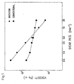
- Figure 1 is a graph showing the viscosity characteristic of a conductive paste of the present invention.
- Figure 2 is a schematic cross-sectional view of a via hole filled with the conductive paste of the present invention.
- Figure 3 is a schematic cross-sectional view of a via hole filled with a conventional conductive paste.
- a conductive paste of the present invention includes an inorganic material component containing conductive material powders and glass powders, an organic vehicle, and a metal organic compound as specified in claim 1.
- the inorganic material component is composed of the conductive material powders for providing a conductive paste with conductivity and the glass powders working as a binder.
- materials used for the conventional conductive paste can be used.
- the conductive material powders include gold, silver, copper, palladium, nickel, ruthenium, platinum, molybdenum, tungsten, and alloys thereof.
- oxides of these metals can be used as the inorganic material component. In this case, the oxide is reduced after the via hole is filled with the paste.
- the conductive material powders have an average particle size preferably in the range of 0.5 to 50 ⁇ m, and more preferably in the range of 5 to 10 ⁇ m.
- the glass powders are softened at temperatures higher than a sintering initiation temperature of a green sheet insulating material.
- the glass powders have an average particle size preferably in the range of 0.1 to 20 ⁇ m, and more preferably in the range of 0.5 to 5 ⁇ m.
- resins used for the conventional conductive paste dissolved in an organic solvent can be used.
- the resins include polyvinyl butyral, polyvinyl alcohol, or a mixed resin in which at least one of ethyl cellulose, acrylic resin (e.g., methyl methacrylate, isobutyl methacrylate, isodecyl methacrylate, glycidyl methacrylate, or copolymers thereof), and phenol resin is added in an amount of not more than 50% by weight to polyvinyl butyral or polyvinyl alcohol.
- Butyral resin is preferably used. These resins are dissolved in organic solvents to obtain organic vehicles. Any organic solvents which can dissolve these resins can be used.
- Butyl carbitol, butyl carbitol acetate, terpineol, and the like are preferably used as the organic solvent.
- the resin concentration in the organic vehicle is preferably in the range of 3 to 40% by weight and more preferably in the range of 5 to 20% by weight.
- metal organic compound an organic complex of silicon or boron can be used. Specifically, organic acid metal salts, orthosilicate ester (silicon alkoxide), and the like are preferred.
- metal 2-ethylhexanoate is preferred because of its easy commercial availability. Examples of the metal 2-ethylhexanoate include silicon 2-ethylhexanoate, copper 2-ethylhexanoate, silver 2-ethylhexanoate, titanium 2-ethylhexanoate, zirconium 2-ethylhexanoate, and vanadium 2-ethylhexanoate.
- silicon alkoxide examples include tetrabenzyl orthosilicate (silicon tetrabenzoxide), tetramethyl orthosilicate (silicon tetramethoxide), tetraethyl orthosilicate (silicon tetraethoxide), and tetrabutyl orthosilicate (silicon tetrabutoxide).
- Tetrabenzyl orthosilicate is available from Nippon Kineki Co., Ltd. and other orthosilicate compounds are available from Tokyo Kasei Kogyo Co., Ltd., respectively.
- titanium alkoxide (titanic acid ester) having a structure similar to that of silicon alkoxide can also be used.
- metal organic compound is used in the present invention, it is preferred that metal is the same element as that contained in the conductive material powders, glass powders, or ceramics used for an insulating layer.
- metal organic compound organic metal ⁇ -bonded to or ⁇ -bonded to a carbon atom of the organic compound can be used. In the case of using these organic metals, organic metals capable of being dissolved in an organic solvent at high concentration should be selected.
- the conductive paste of the present invention can be obtained by mixing and kneading the above-mentioned materials by a known method: A small amount of metal organic compound is added to a mixture in which the inorganic material component and the organic vehicle are mixed in a ratio used in the conventional conductive paste, whereby the conductive paste of the present invention can be obtained. More specifically, at least 0.5% metal organic compound is contained in the conductive paste to be obtained. In the case where less than 0.5% of the metal organic compound is contained in the conductive paste, the conductive paste to be obtained will not have sufficient thixotropy for a via-fill.
- the conductive paste of the present invention preferably includes 75.0 to 90.5% by weight of the inorganic material component containing conductive material powders and glass powders, 9.0 to 20.0% by weight of the organic vehicle containing the organic binder and the solvent, and 0.5 to 5.0% by weight of the metal organic compound, based on the total weight of the conductive paste.
- a conductive paste having high thixotropy has high viscosity with respect to low-speed deformation such as natural flow and has low viscosity with respect to high-speed deformation caused by rapid force. Because of this characteristic, even though the viscosity with respect to natural flow is increased so as to prevent the center portion of the conductive paste from being recessed in the via-hole because of the leveling, the viscosity resistance of the conductive paste while being filled in the via hole becomes small. As a result, the via hole can be easily filled with the paste without any insufficient filling and filling defect, i.e. the recess of the center portion of the conductive past in the via hole is not caused.
- the conductive paste will have thixotropy by including the metal organic compound as follows: When the metal organic compound is added to the mixture of the inorganic material component and the organic vehicle, the conductive material powders and glass powders contained in the organic vehicle are loosely bonded together to form a gel.
- silver powders 40.8% by weight of silver powders, 40.8% by weight of glass powders, 16.4% by weight of organic vehicle, and 2.0% by weight of tetrabenzyl orthosilicate are sufficiently mixed and kneaded using a three roll mill to obtain a conductive paste.
- silver powders those having an average particle size of about 3 ⁇ m, available from Fukuda Metal Foil & Powder Co., Ltd. are used.
- glass powders GA13 (Trade Name) available from Nippon Electric Glass Co., Ltd. is used.
- organic vehicle terpineol solution in which 5% by weight of butyral resin is dissolved is used.
- the results obtained by measuring the conductive paste with a B-type viscometer will be shown.
- RVTD spindle: SC4-14
- the conductive paste is inserted into a spindle, and the spindle is rotated for a predetermined times.
- the viscosity of the conductive paste is obtained in terms of the resistance of the paste during rotation.
- Figure 1 shows a viscosity curve of the conductive paste of the present invention, obtained by the measurement.
- Figure 1 also shows a viscosity curve of a conventional example for comparison.
- the conductive paste of the present invention when the shear rate is low, the conductive paste of the present invention has high viscosity compared with the conventional conductive paste. In contrast, when the shear rate is high, the conductive paste of the present invention has low viscosity compared with the conventional conductive paste.
- the ratio (thixotropic index) of the viscosity at 20 min -1 to the viscosity at 0.5 min -1 of the conductive paste of the present invention is about three times that of the conventional conductive paste.
- the conductive paste of the present invention has sufficiently large viscosity at a low shear rate (i.e., 0.5 min -1 ) and has small viscosity at a high shear rate (i.e., 20 min -1 ).
- the low shear rate corresponds to the case where the conductive paste is slowly pressured so as to effect the leveling;
- the high shear rate corresponds to the case where the conductive paste is rapidly pressured as in the filling of the via hole.
- the relationship between the added amount of the metal organic compound contained in the conductive paste of the present invention and the thixotropic index is shown in the following Table.
- the table shows the thixotropic index of the conductive paste prepared by the above-mentioned method, when using tetrabenzyl orthosilicate and silicon 2-ethylhexanoate are used as the metal organic compound.
- the addition of merely 0.5% by weight of the metal organic compound brings about marked effects.
- An organic vehicle and benzylbutyl phthalate are respectively prepared.
- a glass ceramic material (MLS 1000, manufactured by Nippon Electric Glass Co., Ltd.) capable of being sintered at 900°C composed of lead borosilicate glass powders and alumina powders and acrylic resin are dissolved in methyl ethyl ketone.
- the organic vehicle and benzylbutyl phthalate are sufficiently mixed by a pot mill. Then, the mixture thus obtained is casted by a doctor blade method to obtain a green sheet insulating layer 4, as shown in Figure 2.
- a via hole 2 is formed by punching.
- the via hole 2 is filled with the conductive paste 1 by squeezing under the condition that the portions of the surface of the green sheet insulating layer 4 other than the via hole 2 is masked.
- relatively strong force such as squeezing is applied to the conductive paste 1 at a high speed
- the viscosity of the conductive paste 1 is decreased while the flowability thereof is increased; therefore, the via hole 2 is filled with the conductive paste 1 without any insufficient filling.
- the conductive paste 1 has high viscosity with respect to force applied at a low speed such as natural flow caused by the gravity and evaporation of the solvent. Therefore, the center portion of the conductive paste 1 filled in the via hole 2 is not recessed.
- a wiring pattern is formed on the green sheet insulating layer 4 by screen printing with a thick film conductive paste for wiring (DD1411, manufactured by Kyoto Elex Co., Ltd.).
- a plurality of green sheet insulating layers 4 with a wiring pattern formed thereon are prepared.
- Each green sheet insulating layer 4 is pressed by heating under the condition of 80°C and 200 kg/cm 2 to obtain a layered body. It is noted that a wiring pattern is not formed on the uppermost layer of the layered body and only the via hole 2 is formed therein.
- a binder is removed from the layered body thus obtained in the air in a heating furnace at a peak temperature of 275°C.
- the peak temperature is retained for 360 minutes.
- the layered body is sintered and baked in the air of the heating furnace at a peak temperature of 900°C. In this case, the peak temperature is retained for 10 minutes.
- a wiring pattern is formed on the uppermost layer with a thick film conductive paste (DD2332H, manufactured by Kyoto Elex Co., Ltd.) by screen printing.
- the layered body is baked at a peak temperature of 900°C to obtain a ceramic multilayer wiring substrate. In this case, the peak temperature is retained for 10 minutes.
- the via hole 2 is filled with a conventional conductive paste 5 to obtain a ceramic multilayer wiring substrate in the same process.
- the center portion of the conductive paste 5 is recessed (recess 3 ) due to the leveling.
- the recess of the conductive paste 5 becomes small after filling.
- it is difficult to fill the via hole 2 with this conductive paste because of its high viscosity, which may lead to a filling defect.
- An organic vehicle and benzylbutyl phthalate are respectively prepared.
- a glass ceramic material (MLS1000, manufactured by Nippon Electric Glass Co., Ltd.) which is the same as that of Example 1 and acrylic resin are dissolved in methyl ethyl ketone.
- the organic vehicle and benzylbutyl phthalate are sufficiently mixed by a pot mill. Then, the mixture thus obtained is casted by a doctor blade method to obtain a green sheet insulating layer 4.
- a via hole 2 is formed by punching.
- the via hole 2 is filled with the conductive paste 1.
- the center portion of the conductive paste 1 filled in the via hole 2 is not recessed.
- a wiring pattern is formed by screen printing with a thick film conductive paste for wiring (DD3100, manufactured by Kyoto Elex Co., Ltd.).
- each green sheet insulating layer 4 is pressed by heating under the condition of 80°C and 200 kg/cm 2 to obtain a layered body. It is noted that a wiring pattern is not formed on the uppermost layer of the layered body and only the via hole 2 is formed therein. A binder is removed from the layered body thus obtained in the air in a heating furnace at a peak temperature of 500°C. The peak temperature is retained for 2 hours.
- a copper oxide which is a conductive material in the layered body is reduced to copper in an atmosphere of hydrogen in the heating furnace at a peak temperature of 250°C.
- the peak temperature is retained for 5 hours.
- the layered body is sintered and baked in an atmosphere of nitrogen in the heating furnace at a peak temperature of 900°C. In this case, the peak temperature is retained for 10 minutes,
- a wiring pattern is formed on the uppermost layer with a thick film conductive paste (QP153, manufactured by Dupont) by screen printing.
- the layered body is baked in an atmosphere of nitrogen at a peak temperature of 900°C to obtain a ceramic multilayer wiring substrate. In this case, the peak temperature is retained for 10 minutes.
- the metal organic compound containing the same element as that of the conductive material powders is used.
- unwanted reaction of the inorganic component is not effected by heating, pressing, and reduction during the production of the multilayer wiring substrate; For this reason, the multilayer wiring substrate to be obtained has stable characteristics.
- the metal of the metal organic compound is not necessarily the same element as that of the conductive material powders.
- the metal of the metal organic compound is not reacted with a material for the green sheet insulating layer under heating, pressing, and reduction conditions during the production of the multilayer wiring substrate.
- the metal organic compound including metals such as silicon, boron, aluminum, and titanium can be used.
- the production of the multilayer wiring substrate using the conductive paste of the present invention is described; However, it should be understood that the present invention can also be applied to the production of a double-sided wiring substrate (thickness of the green sheet is about 0.6 mm or more).
- the conductive paste for being filled in the via hole is described.
- the conductive paste can also be used for forming a wiring pattern. In the past, the end portions of the wiring pattern were deformed due to the leveling when the wiring pattern was formed, resulting in an enlarged wiring pattern. However, the use of the conductive paste according to the present invention can overcome this problem.
Landscapes
- Conductive Materials (AREA)
- Parts Printed On Printed Circuit Boards (AREA)
- Production Of Multi-Layered Print Wiring Board (AREA)
Claims (5)
- Pâte conductrice comprenant :des poudres de matériaux inorganiques contenant des poudres de matériaux conducteurs choisis dans le groupe constitué de l'or, le cuivre, le nickel, le ruthénium, le platine, le molybdène, le tungstène et leurs alliages et oxydes ;un véhicule organique contenant un liant organique et un solvant organique ; eti) 0,5 à 5,0 % en poids d'un sel métallique d'acide organique, dans lequel le sel métallique d'acide organique est un composé choisi dans le groupe constitué de 2-éthylhexanoate de silicium, de 2-éthylhexanoate d'argent, de 2-éthylhexanoate de titane et de 2-éthylhexanoate de vanadium ; ouii) 0,5 à 5,0 % en poids d'un composé choisi dans le groupe constitué d'un complexe organique de silicium ou de bore et d'esters d'orthosilicate, caractérisé en ce que les poudres de matériaux inorganiques comprennent également des poudres de verre et en ce que le liant organique est au moins une résine organique choisie dans le groupe constitué de résine butyralpolyvinylique, de résine d'alcool vinylique, de résine butyral ou d'une résine mélangée dans laquelle au moins l'une des résines acryliques et d'une résine phénolique est ajoutée en une quantité de pas plus de 50 % en poids au polyvinylbutyral ou à l'alcool polyvinylique.
- Pâte conductrice selon la revendication 1, comprenant :75,0 à 90,5 % en poids des poudres de matériaux inorganiques ;9,0 à 20,0 % en poids du constituant de véhicule organique ; et0,5 à 5,0 % en poids de i) ou ii).
- Pâte conductrice selon la revendication 2, dans laquelle les poudres de matériaux conducteurs contiennent le même métal que celui contenu dans le composé organique métallique i) ou ii).
- Pâte conductrice selon la revendication 1(ii), dans laquelle le composé organique métallique est un ester d'orthosilicate et l'ester d'orthbsilicate est l'alkoxyde de silicium.
- Pâte conductrice selon la revendication 4, dans laquelle l'alkoxyde de silicium est un composé choisi dans le groupe constitué d'orthosilicate de tétrabenzyle, d'orthosilicate de tétraméthyle, d'orthosilicate de tétraéthyle et d'orthosilicate de tétrabutyle.
Applications Claiming Priority (3)
| Application Number | Priority Date | Filing Date | Title |
|---|---|---|---|
| JP5108492A JP3015621B2 (ja) | 1993-05-10 | 1993-05-10 | 導体ペ−スト組成物 |
| JP108492/93 | 1993-05-10 | ||
| JP10849293 | 1993-05-10 |
Publications (2)
| Publication Number | Publication Date |
|---|---|
| EP0624902A1 EP0624902A1 (fr) | 1994-11-17 |
| EP0624902B1 true EP0624902B1 (fr) | 2002-07-10 |
Family
ID=14486152
Family Applications (1)
| Application Number | Title | Priority Date | Filing Date |
|---|---|---|---|
| EP94107288A Expired - Lifetime EP0624902B1 (fr) | 1993-05-10 | 1994-05-10 | Pâte conductrice thixotropique |
Country Status (5)
| Country | Link |
|---|---|
| US (2) | US5503777A (fr) |
| EP (1) | EP0624902B1 (fr) |
| JP (1) | JP3015621B2 (fr) |
| KR (1) | KR0157238B1 (fr) |
| DE (1) | DE69430935T2 (fr) |
Families Citing this family (29)
| Publication number | Priority date | Publication date | Assignee | Title |
|---|---|---|---|---|
| KR100268699B1 (ko) * | 1996-06-25 | 2000-11-01 | 이.아이,듀우판드네모아앤드캄파니 | 칩저항기터미날전극용전도성페이스트조성물 |
| US5783113A (en) * | 1997-03-27 | 1998-07-21 | International Business Machines Corporation | Conductive paste for large greensheet screening including high thixotropic agent content |
| CN1282202C (zh) * | 1997-04-08 | 2006-10-25 | 松下电器产业株式会社 | 导电糊膏及其生产方法以及用其制成的印刷线路板 |
| WO2003003381A1 (fr) * | 1997-09-12 | 2003-01-09 | Parelec, Inc. | Procede et compositions pour la realisation de conducteurs electriques a basse temperature |
| US6071437A (en) * | 1998-02-26 | 2000-06-06 | Murata Manufacturing Co., Ltd. | Electrically conductive composition for a solar cell |
| JP3539195B2 (ja) * | 1998-03-25 | 2004-07-07 | 株式会社村田製作所 | 導電ペーストおよびそれを用いたセラミック基板の製造方法 |
| US6329059B1 (en) * | 1999-11-12 | 2001-12-11 | Amsil Ltd. | Polymeric composition having self-extinguishing properties |
| JP2001189234A (ja) * | 1999-12-28 | 2001-07-10 | Tdk Corp | 積層コンデンサ |
| KR100348498B1 (ko) * | 2000-07-13 | 2002-08-09 | 명지대학교 | 전자파차폐용 코팅재의 제조방법 |
| JP2002042551A (ja) * | 2000-07-21 | 2002-02-08 | Murata Mfg Co Ltd | スクリーン印刷用ペースト、スクリーン印刷方法及び厚膜焼成体 |
| US7115218B2 (en) | 2001-06-28 | 2006-10-03 | Parelec, Inc. | Low temperature method and composition for producing electrical conductors |
| US6661566B2 (en) | 2001-09-20 | 2003-12-09 | The United States Of America As Represented By The Secretary Of The Navy | Method and optical switch for altering an electromagnetic energy wave in response to acceleration forces |
| US6459055B1 (en) | 2001-09-25 | 2002-10-01 | The United States Of America As Represented By The Secretary Of The Navy | Acceleration responsive switch |
| TWI251018B (en) * | 2002-04-10 | 2006-03-11 | Fujikura Ltd | Electroconductive composition, electroconductive coating and method of producing the electroconductive coating |
| US7387827B2 (en) * | 2002-12-17 | 2008-06-17 | Intel Corporation | Interconnection designs and materials having improved strength and fatigue life |
| US7521115B2 (en) * | 2002-12-17 | 2009-04-21 | Intel Corporation | Low temperature bumping process |
| US7147804B2 (en) * | 2003-01-24 | 2006-12-12 | E. I. Du Pont De Nemours And Company | Terminal electrode compositions for multilayer ceramic capacitors |
| EP1443532A1 (fr) * | 2003-01-24 | 2004-08-04 | E.I.Du pont de nemours and company | Compositions pour électrodes terminales de condensateurs céramiques multicouches |
| US7083744B2 (en) * | 2003-01-24 | 2006-08-01 | E. I. Du Pont De Nemours And Company | Terminal electrode compositions for multilayer ceramic capacitors |
| US7074349B2 (en) * | 2003-01-24 | 2006-07-11 | E. I. Du Pont De Nemours And Company | Terminal electrode compositions for multilayer ceramic capacitors |
| US7279217B2 (en) * | 2004-05-24 | 2007-10-09 | Tdk Corporation | Multilayer ceramic device, method for manufacturing the same, and ceramic device |
| JP4518885B2 (ja) * | 2004-09-09 | 2010-08-04 | 京セラ株式会社 | セラミック電子部品及びその製造方法 |
| GB0515088D0 (en) * | 2005-07-22 | 2005-08-31 | Imerys Minerals Ltd | Particulate glass compositions and methods of production |
| US20080233416A1 (en) * | 2007-01-26 | 2008-09-25 | Kyocera Corporation | Paste composition, green ceramic body, and methods for manufacturing ceramic structure |
| TWI493605B (zh) * | 2008-06-11 | 2015-07-21 | Ind Tech Res Inst | 背面電極層的製造方法 |
| WO2010141519A1 (fr) * | 2009-06-01 | 2010-12-09 | Add-Vision, Inc. | Processus et structure d'encapsulation pour dispositifs electroniques |
| SG189537A1 (en) * | 2010-10-28 | 2013-06-28 | Heraeus Precious Metals North America Conshohocken Llc | Solar cell metallizations containing metal additive |
| WO2014143627A1 (fr) * | 2013-03-14 | 2014-09-18 | Dow Corning Corporation | Compositions de silicone vulcanisables, adhésif de silicone électro-conducteur, procédé de fabrication et d'utilisation associé, et dispositifs électriques associés |
| US9428680B2 (en) * | 2013-03-14 | 2016-08-30 | Dow Corning Corporation | Conductive silicone materials and uses |
Family Cites Families (20)
| Publication number | Priority date | Publication date | Assignee | Title |
|---|---|---|---|---|
| US3056684A (en) * | 1959-06-04 | 1962-10-02 | Carboline Co | Protective coatings |
| US3776741A (en) * | 1970-12-28 | 1973-12-04 | Corning Glass Works | Flame-proof protective coating for electrical film resistors |
| US3819439A (en) * | 1971-05-17 | 1974-06-25 | Hexcel Corp | Method of making honeycomb of sinterable material employing stepwise coating of a resin-containing composition |
| GB1412341A (en) * | 1973-01-29 | 1975-11-05 | Atomic Energy Authority Uk | Metallising pastes |
| FR2296988A1 (fr) * | 1974-12-31 | 1976-07-30 | Ibm France | Perfectionnement aux procedes de fabrication d'un module de circuits multicouches en ceramique |
| US4122143A (en) * | 1976-05-24 | 1978-10-24 | Mitsui Toatsu Chemicals, Inc. | Process for producing cured products |
| US4417007A (en) * | 1981-06-30 | 1983-11-22 | Elkem Metals Company | Zinc rich paint formulations employing manganomanganic oxide fume pigment |
| JPS6286602A (ja) * | 1985-10-09 | 1987-04-21 | 昭栄化学工業株式会社 | 厚膜ペ−スト |
| CA1273853C (fr) * | 1986-12-17 | 1990-09-11 | Methode de production d'une carte ceramique a circuit | |
| DE68912932T2 (de) * | 1989-05-12 | 1994-08-11 | Ibm Deutschland | Glas-Keramik-Gegenstand und Verfahren zu dessen Herstellung. |
| US5135829A (en) * | 1989-10-23 | 1992-08-04 | Ricoh Company, Ltd. | Electrophotographic photoconductor having intermediate layer comprising modified indium oxide |
| JP2795712B2 (ja) * | 1990-02-02 | 1998-09-10 | イビデン株式会社 | スルーホールを有するセラミックス基板の製造方法 |
| US5137560A (en) * | 1990-03-09 | 1992-08-11 | Asahi Glass Company, Inc. | Process for manufacturing glass with functional coating |
| JP2839326B2 (ja) * | 1990-03-28 | 1998-12-16 | 京セラ株式会社 | 磁器電子部品 |
| US5186743A (en) * | 1990-12-13 | 1993-02-16 | Akzo N.V. | Low volatile organic content hybrid silica binder |
| US5216207A (en) * | 1991-02-27 | 1993-06-01 | David Sarnoff Research Center, Inc. | Low temperature co-fired multilayer ceramic circuit boards with silver conductors |
| JPH0520920A (ja) * | 1991-06-20 | 1993-01-29 | Matsushita Electric Ind Co Ltd | 導電性ペーストおよびこれを用いた実装基板 |
| US5156674A (en) * | 1991-06-21 | 1992-10-20 | Mooney Chemicals, Inc. | Drier promoter compositions |
| US5167701A (en) * | 1992-05-22 | 1992-12-01 | Savin Roland R | Zinc-rich coating composition with inorganic binder |
| US5338348A (en) * | 1993-09-22 | 1994-08-16 | Savin Roland R | Zinc powder-rich coating composition |
-
1993
- 1993-05-10 JP JP5108492A patent/JP3015621B2/ja not_active Expired - Fee Related
-
1994
- 1994-05-07 KR KR1019940009968A patent/KR0157238B1/ko not_active Expired - Fee Related
- 1994-05-10 EP EP94107288A patent/EP0624902B1/fr not_active Expired - Lifetime
- 1994-05-10 US US08/240,376 patent/US5503777A/en not_active Expired - Lifetime
- 1994-05-10 DE DE69430935T patent/DE69430935T2/de not_active Expired - Fee Related
-
1995
- 1995-12-26 US US08/581,352 patent/US5688441A/en not_active Expired - Lifetime
Also Published As
| Publication number | Publication date |
|---|---|
| US5688441A (en) | 1997-11-18 |
| JPH06326433A (ja) | 1994-11-25 |
| DE69430935T2 (de) | 2003-01-30 |
| JP3015621B2 (ja) | 2000-03-06 |
| EP0624902A1 (fr) | 1994-11-17 |
| KR0157238B1 (ko) | 1998-11-16 |
| US5503777A (en) | 1996-04-02 |
| DE69430935D1 (de) | 2002-08-14 |
Similar Documents
| Publication | Publication Date | Title |
|---|---|---|
| US5688441A (en) | Thixotropic conductive paste | |
| US7611645B2 (en) | Thick film conductor compositions and the use thereof in LTCC circuits and devices | |
| JP3226280B2 (ja) | 多層回路板の製造方法 | |
| US6667256B2 (en) | Glass-ceramic composition for ceramic electronic part, ceramic electronic part, and method for manufacturing multilayer ceramic electronic part | |
| EP1981320B1 (fr) | Pâte conductrice, substrat céramique multicouche et procédé de fabrication d'un substrat céramique multicouche | |
| EP0519175A2 (fr) | Procédé de fabrication de circuits électroniques multicouches | |
| EP1717858A1 (fr) | Compositions de pâtes conductrices à couche épaisse pour bande LTCC pour applications dans le domaine des micro-ondes | |
| JP3467872B2 (ja) | 多層セラミック基板の製造方法 | |
| EP0591733A1 (fr) | Procédé pour la fabrication d'un substrat céramique multi-couche | |
| US9307649B2 (en) | Mixed-metal system conductors for use in low-temperature co-fired ceramic circuits and devices | |
| EP0591604B1 (fr) | Compositions pour le remplissage des trous d'interconnexion | |
| JP3098288B2 (ja) | 導体組成物およびそれを用いたセラミック基板 | |
| JP2735776B2 (ja) | 多層アルミナ質配線基板及び半導体素子収納用パッケージ | |
| KR0173553B1 (ko) | 비어 충전 및 포착 패드 첩부용 후막 조성물 | |
| JP2004273426A (ja) | 導電ペーストおよびそれを用いたセラミック多層基板 | |
| JP3188086B2 (ja) | セラミック配線基板とその製造方法及びその実装構造 | |
| JPS61278195A (ja) | 多層回路基板及びその製造方法 | |
| JPH0878847A (ja) | 低温焼成多層回路基板 | |
| JP3529495B2 (ja) | 窒化アルミニウムセラミックス基板及びその製造方法 | |
| JPH06338686A (ja) | 多層基板の製造方法 | |
| JPH06139814A (ja) | 導体ペースト | |
| JPH0793480B2 (ja) | 多層ガラスセラミック基板とその製造方法 | |
| JPH0969687A (ja) | ガラスセラミック多層配線基板の製造方法 | |
| JPH05275861A (ja) | 多層回路基板 | |
| JP2004146394A (ja) | ガラスセラミック配線基板 |
Legal Events
| Date | Code | Title | Description |
|---|---|---|---|
| PUAI | Public reference made under article 153(3) epc to a published international application that has entered the european phase |
Free format text: ORIGINAL CODE: 0009012 |
|
| 17P | Request for examination filed |
Effective date: 19940914 |
|
| AK | Designated contracting states |
Kind code of ref document: A1 Designated state(s): DE FR GB |
|
| 17Q | First examination report despatched |
Effective date: 19970630 |
|
| GRAG | Despatch of communication of intention to grant |
Free format text: ORIGINAL CODE: EPIDOS AGRA |
|
| GRAG | Despatch of communication of intention to grant |
Free format text: ORIGINAL CODE: EPIDOS AGRA |
|
| GRAH | Despatch of communication of intention to grant a patent |
Free format text: ORIGINAL CODE: EPIDOS IGRA |
|
| GRAH | Despatch of communication of intention to grant a patent |
Free format text: ORIGINAL CODE: EPIDOS IGRA |
|
| GRAA | (expected) grant |
Free format text: ORIGINAL CODE: 0009210 |
|
| AK | Designated contracting states |
Kind code of ref document: B1 Designated state(s): DE FR GB |
|
| REG | Reference to a national code |
Ref country code: GB Ref legal event code: FG4D |
|
| REF | Corresponds to: |
Ref document number: 69430935 Country of ref document: DE Date of ref document: 20020814 |
|
| ET | Fr: translation filed | ||
| PLBE | No opposition filed within time limit |
Free format text: ORIGINAL CODE: 0009261 |
|
| STAA | Information on the status of an ep patent application or granted ep patent |
Free format text: STATUS: NO OPPOSITION FILED WITHIN TIME LIMIT |
|
| 26N | No opposition filed |
Effective date: 20030411 |
|
| PGFP | Annual fee paid to national office [announced via postgrant information from national office to epo] |
Ref country code: FR Payment date: 20090515 Year of fee payment: 16 Ref country code: DE Payment date: 20090511 Year of fee payment: 16 |
|
| PGFP | Annual fee paid to national office [announced via postgrant information from national office to epo] |
Ref country code: GB Payment date: 20090506 Year of fee payment: 16 |
|
| GBPC | Gb: european patent ceased through non-payment of renewal fee |
Effective date: 20100510 |
|
| REG | Reference to a national code |
Ref country code: FR Ref legal event code: ST Effective date: 20110131 |
|
| PG25 | Lapsed in a contracting state [announced via postgrant information from national office to epo] |
Ref country code: DE Free format text: LAPSE BECAUSE OF NON-PAYMENT OF DUE FEES Effective date: 20101201 |
|
| PG25 | Lapsed in a contracting state [announced via postgrant information from national office to epo] |
Ref country code: FR Free format text: LAPSE BECAUSE OF NON-PAYMENT OF DUE FEES Effective date: 20100531 |
|
| PG25 | Lapsed in a contracting state [announced via postgrant information from national office to epo] |
Ref country code: GB Free format text: LAPSE BECAUSE OF NON-PAYMENT OF DUE FEES Effective date: 20100510 |