EP0625801A1 - Electrode ohmique et procédé pour sa fabrication - Google Patents
Electrode ohmique et procédé pour sa fabrication Download PDFInfo
- Publication number
- EP0625801A1 EP0625801A1 EP94106991A EP94106991A EP0625801A1 EP 0625801 A1 EP0625801 A1 EP 0625801A1 EP 94106991 A EP94106991 A EP 94106991A EP 94106991 A EP94106991 A EP 94106991A EP 0625801 A1 EP0625801 A1 EP 0625801A1
- Authority
- EP
- European Patent Office
- Prior art keywords
- layer
- metallic layer
- compound semiconductor
- metallic
- ohmic electrode
- Prior art date
- Legal status (The legal status is an assumption and is not a legal conclusion. Google has not performed a legal analysis and makes no representation as to the accuracy of the status listed.)
- Granted
Links
Images


Classifications
-
- H—ELECTRICITY
- H10—SEMICONDUCTOR DEVICES; ELECTRIC SOLID-STATE DEVICES NOT OTHERWISE PROVIDED FOR
- H10D—INORGANIC ELECTRIC SEMICONDUCTOR DEVICES
- H10D64/00—Electrodes of devices having potential barriers
- H10D64/01—Manufacture or treatment
- H10D64/011—Manufacture or treatment of electrodes ohmically coupled to a semiconductor
- H10D64/0116—Manufacture or treatment of electrodes ohmically coupled to a semiconductor to Group III-V semiconductors
-
- H—ELECTRICITY
- H10—SEMICONDUCTOR DEVICES; ELECTRIC SOLID-STATE DEVICES NOT OTHERWISE PROVIDED FOR
- H10D—INORGANIC ELECTRIC SEMICONDUCTOR DEVICES
- H10D64/00—Electrodes of devices having potential barriers
- H10D64/60—Electrodes characterised by their materials
- H10D64/62—Electrodes ohmically coupled to a semiconductor
-
- H—ELECTRICITY
- H10—SEMICONDUCTOR DEVICES; ELECTRIC SOLID-STATE DEVICES NOT OTHERWISE PROVIDED FOR
- H10D—INORGANIC ELECTRIC SEMICONDUCTOR DEVICES
- H10D62/00—Semiconductor bodies, or regions thereof, of devices having potential barriers
- H10D62/80—Semiconductor bodies, or regions thereof, of devices having potential barriers characterised by the materials
- H10D62/85—Semiconductor bodies, or regions thereof, of devices having potential barriers characterised by the materials being Group III-V materials, e.g. GaAs
Definitions
- the present invention relates to an ohmic electrode suitable for use in compound semiconductor devices.
- an ohmic electrode of a gallium arsenide (GaAs)-based compound semiconductor device is formed on a GaAs-based semiconductor layer or a GaAs substrate by subjecting a Ni/Au-Ge metallic layer to alloying treatment. More specifically, an ohmic electrode can be formed, for example, by depositing an Au-(12 wt.%)Ge layer, then a nickel layer thereon by means of vacuum deposition process, and alloying the resulting metallic layer by heating it at a temperature range of from 400 to 450°C for a duration of 1 to 2 minutes.
- the Au-Ge alloy is molten to form a liquid phase at a temperature not lower than the eutectic point of 356 °C. Because the surface of an n-type GaAs compound semiconductor layer is unsaturated, gallium and arsenic dissolve into the Au-Ge melt during the alloying treatment. Thus is formed an alloy layer comprising, in addition to an Au-Ga alloy, a Ni-As-Ge alloy which results from arsenic, nickel, and germanium that are present in excess. During lowering the temperature, that is, during the re-growth of GaAs, germanium is incorporated into GaAs to occupy the vacancy sites of gallium (Ga) to form an n+ layer.
- Nickel plays a role of absorbing gold and germanium to form a film of Ni-Au-Ge alloy, and of preventing boring up of Au-Ge alloy.
- An electrode material layer is deposited thereafter on the alloy layer, and is etched into a desired shape to obtain a complete ohmic electrode.
- An ohmic contact between the metallic Ni/Au-Ge layer and the base layer, i.e., the GaAs-based semiconductor layer or the GaAs-based substrate, can be formed by alloying the metallic Ni/Au-Ge layer as described above.
- the heat treatment for the alloying must be performed at a temperature in the range of from 400 to 450 °C for a duration of 1 to 2 minutes.
- the temperature of alloying is sufficiently lower than, for example, the crystal growth temperature for GaAs considering that an MOCVD process is effected at about 800 °C.
- alloying was believed to be free of problems, i.e., to have no influence on ion implantation and other processes for fabricating compound semiconductor devices.
- Group II-VI compound semiconductor a compound consisting of a Group II and a Group VI element of periodic table (hereinafter referred to simply as a "Group II-VI compound semiconductor") on an n-type GaAs substrate
- the temperature during the process is maintained at 300 °C or lower. Therefore, problems are encountered in forming an ohmic electrode on the back of an n-type GaAs substrate, because crystal defects and the like generate on the Group II-VI compound semiconductor layer due to the heat treatment, and the crystallinity of the Group II-VI compound semiconductor layer is impaired unfavorably by these defects.
- An organic thin film such as of polyimide is used in an optoelectronic integrated device comprising thereon a laser element and an optical waveguide.
- the organic thin films cannot resist to a heat treatment performed at such a high temperature of 400 °C or even higher.
- such an alloying treatment is problematic in that it generates thermal stress on optical waveguides.
- an object of the present invention is to provide an ohmic electrode suitable for use in compound semiconductor devices, and a process for fabricating the same, which realizes a favorable ohmic contact by a low-temperature alloying treatment that can be effected at a relatively low temperature of 350 °C or lower.
- an ohmic electrode according to the present invention characterized in that it is obtained by a process comprising forming a first metallic layer of indium or an indium alloy on a compound semiconductor layer, further forming a second metallic layer of gold-germanium alloy on the first metallic layer, and subjecting the first and the second metallic layers to alloying treatment.
- compound semiconductor layer as referred herein not only signifies the compound semiconductor layer formed on an compound semiconductor substrate, but also encompasses the compound semiconductor substrate itself.
- the ohmic electrode according to the present invention preferably comprises a third metallic layer made of nickel, being formed either on a second metallic layer or interposed between a first and a second metallic layer, so that an ohmic electrode can be obtained by alloying the first, the second, and the third metallic layer.
- the first metallic layer is preferably formed at a thickness of from 2 nm to 50 nm. If the first metallic layer is formed at a thickness of less than 2 nm, an ohmic contact cannot be realized between the compound semiconductor layer and the metallic layer upon alloying at a temperature of 350 °C or lower. If the first metallic layer is formed at a thickness exceeding 50 nm, on the other hand, the alloying process becomes too time-consuming.
- a process for fabricating an ohmic contact comprising: forming a first metallic layer comprising indium or an indium alloy on a compound semiconductor layer; forming a second metallic layer comprising a gold-germanium alloy on said first metallic layer; and subjecting said first metallic layer and said second metallic layer to alloying treatment at a temperature of 350 °C or lower.
- the alloying treatment is effected by heating, as mentioned above, at a temperature of 350 °C or lower, preferably at 320 °C or lower, and more preferably, at 300 °C or lower.
- the duration of heating is set longer with increasing thickness of the first metallic layer.
- the lower limit of the heating temperature is determined by measuring the contact resistivity of a contact between the electrode and the compound semiconductor layer provided as a base, however, it is generally higher than 250 °C. If the heating temperature should exceed 350 °C, the crystallinity of the Group II-VI compound semiconductor becomes impaired; in the case of an optoelectronic device, furthermore, damages occur on the material used, or thermal stress is generated on the optical waveguide.
- the heating temperature should be 250 °C or lower, melting into the first metallic layer occurs only insufficiently to prevent contact from forming between the compound semiconductor layer and the second metallic layer. In the latter case, the contact resistivity of the contact between the electrode and the compound semiconductor layer increases unfavorably.
- the process for forming an ohmic contact according to the present invention comprises forming a third metallic layer using nickel after forming a first metallic layer made of an indium or an indium alloy on a compound semiconductor layer, or after forming a second metallic layer made of a gold-germanium alloy on the first metallic layer.
- the step of alloying the first, the second, and the third metallic layer is preferably effected at a temperature not higher than 350 °C.
- the first metallic layer is preferably formed at a thickness of from 2 to 50 nm.
- the melting point of indium is 156 °C.
- the first metallic layer of indium or an indium alloy undergoes melting at a temperature lower than the eutectic point (356 °C) of the gold-germanium alloy.
- the compound semiconductor layer provided as the base layer and the upper second metallic layer dissolve into the molten first metallic layer to form altogether an alloy layer.
- an electrode is obtained from the resulting alloy layer, and this alloy layer also forms an ohmic contact between the compound semiconductor layer provided as the base.
- Ga 1-x In x As is produced by melting the first metallic layer and the compound semiconductor layer provided as the base.
- This Ga 1-x In x As layer has a band gap lower than that of GaAs, and exhibits a nature more similar to that of a metal. Accordingly, the use of Ga 1-x In x As lowers the contact resistivity.
- a GaAs compound semiconductor is fabricated at first by using a conventional process.
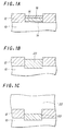
- FIG. 1A which shows schematically a partial cross section view of the structure
- an epitaxially grown n+-type GaAs compound semiconductor layer 10 is provided as an uppermost layer on a compound semiconductor substrate.
- the practical structure comprises a buffer layer, a p-type clad, an active layer, and an n-type clad formed in this order from the substrate side between the compound semiconductor substrate and the compound semiconductor layer 10.
- an insulating layer 12 made of, for example, SiN, is formed on the compound semiconductor layer 10 in the regions other than those on which the ohmic electrode is to be formed.
- the insulating layer 12 is formed by an ordinary CVD process and the like. This insulating layer 12 may be omitted in some cases.
- a first metallic layer 14 made of indium (In), a second metallic layer 16 made of a gold-germanium alloy containing 12 % by weight of germanium, and a third metallic layer 18 made of nickel are formed on the compound semiconductor layer 10 by, for example, vapor deposition assisted by electron beam heating or resistance heating, or any of the known film deposition processes.
- the metallic layer is patterned thereafter by lift-off process.
- the first metallic layer 14, the second metallic layer 16, and the third metallic layer 18 were each formed at a thickness of 10 nm, 170 nm, and 40 nm, respectively, to obtain a structure shown in FIG. 1A.
- the first, the second, and the third metallic layer are subjected to alloying treatment at a temperature not higher than 350 °C to form an alloy layer 20.
- the temperature and the duration of the alloying treatment can be modified properly depending on the individual case.
- an alloy can be obtained through the reaction between the metallic layers 14, 16, and 18, specifically, In/Au-Ge/Ni layers to obtain a structure shown in FIG. 1B.
- FIG. 1B Thus is an ohmic electrode implemented.
- the alloying treatment can be effected by furnace alloying, which comprises elevating and lowering the temperature of a furnace, by RTA (Rapid Thermal Annealing) alloying using an infrared radiation lamp and the like, or by any known process, under a controlled atmosphere using various types of gases, such as an inert gas (e.g., nitrogen and argon) or a mixed gas using two or more thereof, or a mixed gas containing an inert gas mixed with hydrogen gas, or hydrogen gas alone.
- furnace alloying which comprises elevating and lowering the temperature of a furnace, by RTA (Rapid Thermal Annealing) alloying using an infrared radiation lamp and the like, or by any known process, under a controlled atmosphere using various types of gases, such as an inert gas (e.g., nitrogen and argon) or a mixed gas using two or more thereof, or a mixed gas containing an inert gas mixed with hydrogen gas, or hydrogen gas alone.
- inert gas e.g., nitrogen and argon
- an electrode material layer 22 is formed on the alloy layer 20 by means of a known process to obtain a structure shown in FIG. 1C.
- the electrode material layer 22 may comprise, in this order from the alloy layer 20 side, a 50 nm thick titanium layer, a 50 nm thick tungsten layer, a 50 nm thick titanium layer, a 50 nm thick platinum layer, and a 500 nm thick gold layer. These layers can be deposited by, for example, vapor deposition.
- the thus obtained electrode material is then patterned by ion-milling and the like to obtain an electrode shaped as desired.
- the lowermost titanium layer is provided for improving the adhesion strength of the electrode material layer with respect to the alloy layer 20, and the tungsten layer is incorporated to prevent intermetallic reaction from occurring between the lower layers and the upper layers (titanium-platinum-gold layer in this case).
- Specimens of ohmic electrode were fabricated according to the described process.
- the alloying temperature was varied to 250 °C, 300 °C, 350 °C, and 400 °C while maintaining the process duration constant to 10 minutes.
- the contact resistivity of the contact between the electrode and the compound semiconductor of the thus obtained specimens was measured according to TLM method described in R. Williams, " Modern GaAs Processing Methods ", Artech House (1990), pp 227. The results are given in FIG. 2A. The observed values are plotted with open circles in the graph.
- the contact resistivity of the contact between the electrode and the compound semiconductor layer of the thus obtained comparative ohmic electrodes was measured by the TLM method. The results are plotted with open rhombohedra in the graph of FIG. 2A.
- FIG. 2A reads clearly that the ohmic electrode fabricated according to the process of the present invention effected at an alloying temperature of 300 °C yield a lower contact resistivity as compared to one obtained by a prior art process.
- specimens of ohmic electrode were fabricated each by setting the alloying temperature to 260 °C, 280 °C, 300 °C, and 320 °C.
- the contact resistivity of the contact between the electrode and the compound semiconductor of the thus obtained ohmic electrode specimens was measured by TLM method. The results are plotted with open circles in the graph of FIG. 2B. For instance, a specimen fabricated by alloying at a temperature of 300 °C and for a duration of 5 minutes was found to yield a contact resistivity Rc of about 2 x 10 ⁇ 5 [ ⁇ cm2].
- ohmic electrodes were fabricated in a similar process as in the fabrication of the specimens above, except for not providing the first metallic layer, and for effecting the alloying treatment for a duration of 90 seconds.
- the contact resistivity of the contact between the electrode and the compound semiconductor layer of the thus obtained comparative ohmic electrodes was measured by the TLM method. The results are plotted with open rhombohedra in the graph shown in FIG. 2B.
- a comparative ohmic electrode obtained by an alloying treatment at 300 °C and for a duration of 90 seconds yielded a contact resistivity Rc of about 1 x 10 ⁇ 4 [ ⁇ cm2], which is about 5 times as large as the value obtained for an ohmic electrode according to the present invention.
- FIG. 3 shows the change of contact resistivity of a contact between the electrode and the compound semiconductor with varying thicknesses of the first metallic layer for both ohmic electrodes according to the present invention and to a prior art.
- the alloying treatment was performed on all of the specimens at 300 °C.
- the observed value for an ohmic electrode of a conventional type obtained by alloying for a duration of 90 seconds and having no first metallic layer is plotted with an open rhombohedron.
- the values plotted with an open circle are for the ohmic electrodes according to the present invention, and the alloying treatment in those electrodes was performed for a duration of 10 minutes.
- the value plotted with a filled circle is also for an ohmic electrode according to the present invention, however, the alloying treatment was performed for a duration of 40 minutes. It can be seen from FIG. 3 that the contact resistivity is lowered as compared to those of the prior art ohmic electrodes by providing the first metallic layer at a thickness of from about 2 to 50 nm.
- the metallic layer structure prior to the alloying treatment for forming the ohmic electrode can be modified as illustrated in FIG. 4.
- a third metallic layer 18 is interposed between a first metallic layer 14 and a second metallic layer 16.
- FIG. 4B there is shown a structure in which the third metallic layer is omitted.
- the first metallic layer can be formed not only by using indium alone, but also by using indium based alloys such as an indium-gold alloy and an indium-germanium alloy.
- the compound semiconductor layer can be made of any compound semiconductor formed from an Ni/Au-Ge alloy layer in a prior art ohmic electrode, such as Ga 1-x In x As and Al 1-x Ga x As.
- the thickness of the first and the third metallic layer is not only limited to those specified in the example above, and can be properly modified as desired.
- the ohmic electrode according to the present invention can be applied to n-type electrodes to be formed on the back of n-type compound semiconductor substrates.
- the present invention comprises forming a first metallic layer made of indium or an indium alloy, and realizes an ohmic electrode at an alloying temperature sufficiently lower than any achieved by a conventional process. Accordingly, the crystallinity of the Group II-VI compound semiconductor layer can be favorably maintained, and the problems, for example, of causing thermal damage on the material used in optoelectronic integrated devices and of generating thermal stress on optical waveguides in the same, can be prevented from occurring.
Landscapes
- Electrodes Of Semiconductors (AREA)
Applications Claiming Priority (2)
| Application Number | Priority Date | Filing Date | Title |
|---|---|---|---|
| JP136708/93 | 1993-05-14 | ||
| JP5136708A JPH06326051A (ja) | 1993-05-14 | 1993-05-14 | オーミック電極及びその形成方法 |
Publications (2)
| Publication Number | Publication Date |
|---|---|
| EP0625801A1 true EP0625801A1 (fr) | 1994-11-23 |
| EP0625801B1 EP0625801B1 (fr) | 1998-12-16 |
Family
ID=15181636
Family Applications (1)
| Application Number | Title | Priority Date | Filing Date |
|---|---|---|---|
| EP94106991A Expired - Lifetime EP0625801B1 (fr) | 1993-05-14 | 1994-05-04 | Méthode de fabrication d'une électrode ohmique |
Country Status (6)
| Country | Link |
|---|---|
| US (1) | US5387549A (fr) |
| EP (1) | EP0625801B1 (fr) |
| JP (1) | JPH06326051A (fr) |
| DE (1) | DE69415210T2 (fr) |
| MY (1) | MY111096A (fr) |
| TW (1) | TW281779B (fr) |
Families Citing this family (4)
| Publication number | Priority date | Publication date | Assignee | Title |
|---|---|---|---|---|
| US5924002A (en) * | 1994-12-22 | 1999-07-13 | Sony Corporation | Method of manufacturing a semiconductor device having ohmic electrode |
| US5646069A (en) * | 1995-06-07 | 1997-07-08 | Hughes Aircraft Company | Fabrication process for Alx In1-x As/Gay In1-y As power HFET ohmic contacts |
| JPH11274468A (ja) * | 1998-03-25 | 1999-10-08 | Sony Corp | オーミック電極およびその形成方法ならびにオーミック電極形成用積層体 |
| JP6206159B2 (ja) | 2013-12-17 | 2017-10-04 | 三菱電機株式会社 | 半導体装置の製造方法 |
Citations (2)
| Publication number | Priority date | Publication date | Assignee | Title |
|---|---|---|---|---|
| EP0037005A1 (fr) * | 1980-03-27 | 1981-10-07 | Siemens Aktiengesellschaft | Contact à basse résistance sans effet de redressement sur du matériel semiconducteur III-V et procédé de fabrication |
| EP0042066A2 (fr) * | 1980-06-12 | 1981-12-23 | International Business Machines Corporation | Dispositif semi-conducteur intermétallique |
Family Cites Families (3)
| Publication number | Priority date | Publication date | Assignee | Title |
|---|---|---|---|---|
| JPS5624928A (en) * | 1979-08-09 | 1981-03-10 | Nippon Telegr & Teleph Corp <Ntt> | Electrode forming method of semiconductor |
| US4662060A (en) * | 1985-12-13 | 1987-05-05 | Allied Corporation | Method of fabricating semiconductor device having low resistance non-alloyed contact layer |
| US4794444A (en) * | 1986-04-10 | 1988-12-27 | General Electric Company | Ohmic contact and method for making same |
-
1993
- 1993-05-14 JP JP5136708A patent/JPH06326051A/ja active Pending
-
1994
- 1994-05-04 EP EP94106991A patent/EP0625801B1/fr not_active Expired - Lifetime
- 1994-05-04 DE DE69415210T patent/DE69415210T2/de not_active Expired - Fee Related
- 1994-05-10 TW TW083104224A patent/TW281779B/zh active
- 1994-05-11 MY MYPI94001183A patent/MY111096A/en unknown
- 1994-05-13 US US08/242,430 patent/US5387549A/en not_active Expired - Fee Related
Patent Citations (2)
| Publication number | Priority date | Publication date | Assignee | Title |
|---|---|---|---|---|
| EP0037005A1 (fr) * | 1980-03-27 | 1981-10-07 | Siemens Aktiengesellschaft | Contact à basse résistance sans effet de redressement sur du matériel semiconducteur III-V et procédé de fabrication |
| EP0042066A2 (fr) * | 1980-06-12 | 1981-12-23 | International Business Machines Corporation | Dispositif semi-conducteur intermétallique |
Non-Patent Citations (4)
| Title |
|---|
| "Preparing thermally stable ohmic contacts for gallium arsenide semiconductor devices", IBM TECHNICAL DISCLOSURE BULLETIN, vol. 31, no. 2, July 1988 (1988-07-01), NEW YORK US, pages 383 - 384 * |
| A. CHRISTOU: "Solid phase formation in Au:Ge/Ni, Ag/In/Ge, In/Au:Ge GaAs ohmic contact systems", SOLID STATE ELECTRONICS, vol. 22, no. 2, February 1979 (1979-02-01), OXFORD GB, pages 141 - 149, XP025820789, DOI: doi:10.1016/0038-1101(79)90106-0 * |
| D.K. JADUS ET AL.: "Ohmic contacts to GaAs by a simple low temperature alloying process", JOURNAL OF THE ELECTROCHEMICAL SOCIETY, vol. 114, no. 4, April 1967 (1967-04-01), MANCHESTER, NEW HAMPSHIRE US, pages 408 - 410 * |
| T. CLAUSEN ET AL.: "Metallurgical optimization to InP using conventional metallization schemes", MICROELECTRONIC ENGINEERING, vol. 18, no. 4, November 1992 (1992-11-01), AMSTERDAM NL, pages 305 - 325, XP024739638, DOI: doi:10.1016/0167-9317(92)90131-A * |
Also Published As
| Publication number | Publication date |
|---|---|
| DE69415210D1 (de) | 1999-01-28 |
| DE69415210T2 (de) | 1999-06-24 |
| TW281779B (fr) | 1996-07-21 |
| MY111096A (en) | 1999-08-30 |
| EP0625801B1 (fr) | 1998-12-16 |
| US5387549A (en) | 1995-02-07 |
| JPH06326051A (ja) | 1994-11-25 |
Similar Documents
| Publication | Publication Date | Title |
|---|---|---|
| US6614115B2 (en) | Enhancement of carrier concentration in As-containing layers | |
| US4186410A (en) | Nonalloyed ohmic contacts to n-type Group III(a)-V(a) semiconductors | |
| US4188710A (en) | Ohmic contacts for group III-V n-type semiconductors using epitaxial germanium films | |
| US4555301A (en) | Formation of heterostructures by pulsed melting of precursor material | |
| US4960728A (en) | Homogenization anneal of II-VI compounds | |
| JPH01289108A (ja) | ヘテロエピタキシャル成長方法 | |
| JPH02285631A (ja) | 特に平面タイプのモノリシック電子コンポーネントの作製のための、半導体の組成又はドーピングの方向付けられた変更のための方法及び対応製品 | |
| US4179534A (en) | Gold-tin-gold ohmic contact to N-type group III-V semiconductors | |
| US5093280A (en) | Refractory metal ohmic contacts and method | |
| US5731224A (en) | Method for manufacturing ohmic contacts for compound semiconductors | |
| US4301188A (en) | Process for producing contact to GaAs active region | |
| EP0093971B1 (fr) | Dispositif semi-conducteur comprenant une couche intermédiaire d'un élément de transition et procédé pour le fabriquer | |
| Paola | Metallic contacts for gallium arsenide | |
| JP2907452B2 (ja) | 化合物半導体用電極 | |
| US5387549A (en) | Process for fabricating ohmic contact | |
| US4757030A (en) | Method of making group IV single crystal layers on group III-V substrates using solid phase epitaxial growth | |
| JPH0139206B2 (fr) | ||
| EP0424857B1 (fr) | Procédé de fabrication d'une électrode ohmique pour nitrure de bore cubique de type P | |
| JP2000277455A (ja) | オーミック電極およびその製造方法 | |
| JPS5877227A (ja) | オ−ミツク接点の形成方法 | |
| JPH0945635A (ja) | 半導体装置の製造方法,及び半導体装置 | |
| US5160793A (en) | Shallow ohmic contacts to n-Alx Ga1-x As | |
| CA2260574A1 (fr) | Contact ohmique et processus de fabrication de ce genre de contact | |
| Okamoto et al. | Fabrication of GaAs‐Mo‐Si structures by metalorganic chemical vapor deposition and laser annealing | |
| EP0247158B1 (fr) | Procede de fabrication d'articles ayant des structures heteroepitaxiales |
Legal Events
| Date | Code | Title | Description |
|---|---|---|---|
| PUAI | Public reference made under article 153(3) epc to a published international application that has entered the european phase |
Free format text: ORIGINAL CODE: 0009012 |
|
| AK | Designated contracting states |
Kind code of ref document: A1 Designated state(s): DE FR GB |
|
| 17P | Request for examination filed |
Effective date: 19950421 |
|
| 17Q | First examination report despatched |
Effective date: 19961223 |
|
| GRAG | Despatch of communication of intention to grant |
Free format text: ORIGINAL CODE: EPIDOS AGRA |
|
| GRAG | Despatch of communication of intention to grant |
Free format text: ORIGINAL CODE: EPIDOS AGRA |
|
| GRAH | Despatch of communication of intention to grant a patent |
Free format text: ORIGINAL CODE: EPIDOS IGRA |
|
| GRAH | Despatch of communication of intention to grant a patent |
Free format text: ORIGINAL CODE: EPIDOS IGRA |
|
| GRAA | (expected) grant |
Free format text: ORIGINAL CODE: 0009210 |
|
| AK | Designated contracting states |
Kind code of ref document: B1 Designated state(s): DE FR GB |
|
| REF | Corresponds to: |
Ref document number: 69415210 Country of ref document: DE Date of ref document: 19990128 |
|
| ET | Fr: translation filed | ||
| PLBE | No opposition filed within time limit |
Free format text: ORIGINAL CODE: 0009261 |
|
| STAA | Information on the status of an ep patent application or granted ep patent |
Free format text: STATUS: NO OPPOSITION FILED WITHIN TIME LIMIT |
|
| 26N | No opposition filed | ||
| PGFP | Annual fee paid to national office [announced via postgrant information from national office to epo] |
Ref country code: DE Payment date: 20010430 Year of fee payment: 8 |
|
| PGFP | Annual fee paid to national office [announced via postgrant information from national office to epo] |
Ref country code: GB Payment date: 20010502 Year of fee payment: 8 |
|
| PGFP | Annual fee paid to national office [announced via postgrant information from national office to epo] |
Ref country code: FR Payment date: 20010518 Year of fee payment: 8 |
|
| REG | Reference to a national code |
Ref country code: GB Ref legal event code: IF02 |
|
| PG25 | Lapsed in a contracting state [announced via postgrant information from national office to epo] |
Ref country code: GB Free format text: LAPSE BECAUSE OF NON-PAYMENT OF DUE FEES Effective date: 20020504 |
|
| PG25 | Lapsed in a contracting state [announced via postgrant information from national office to epo] |
Ref country code: DE Free format text: LAPSE BECAUSE OF NON-PAYMENT OF DUE FEES Effective date: 20021203 |
|
| GBPC | Gb: european patent ceased through non-payment of renewal fee |
Effective date: 20020504 |
|
| PG25 | Lapsed in a contracting state [announced via postgrant information from national office to epo] |
Ref country code: FR Free format text: LAPSE BECAUSE OF NON-PAYMENT OF DUE FEES Effective date: 20030131 |
|
| REG | Reference to a national code |
Ref country code: FR Ref legal event code: ST |