EP0629892A2 - Optische Vorrichtung vom Wellenleitertyp, und Verfahren zur Impedanzpassung dazu - Google Patents
Optische Vorrichtung vom Wellenleitertyp, und Verfahren zur Impedanzpassung dazu Download PDFInfo
- Publication number
- EP0629892A2 EP0629892A2 EP94109074A EP94109074A EP0629892A2 EP 0629892 A2 EP0629892 A2 EP 0629892A2 EP 94109074 A EP94109074 A EP 94109074A EP 94109074 A EP94109074 A EP 94109074A EP 0629892 A2 EP0629892 A2 EP 0629892A2
- Authority
- EP
- European Patent Office
- Prior art keywords
- waveguide
- optical device
- type optical
- impedance
- signal electrode
- Prior art date
- Legal status (The legal status is an assumption and is not a legal conclusion. Google has not performed a legal analysis and makes no representation as to the accuracy of the status listed.)
- Withdrawn
Links
Images



Classifications
-
- H—ELECTRICITY
- H03—ELECTRONIC CIRCUITRY
- H03H—IMPEDANCE NETWORKS, e.g. RESONANT CIRCUITS; RESONATORS
- H03H7/00—Multiple-port networks comprising only passive electrical elements as network components
- H03H7/38—Impedance-matching networks
-
- G—PHYSICS
- G02—OPTICS
- G02F—OPTICAL DEVICES OR ARRANGEMENTS FOR THE CONTROL OF LIGHT BY MODIFICATION OF THE OPTICAL PROPERTIES OF THE MEDIA OF THE ELEMENTS INVOLVED THEREIN; NON-LINEAR OPTICS; FREQUENCY-CHANGING OF LIGHT; OPTICAL LOGIC ELEMENTS; OPTICAL ANALOGUE/DIGITAL CONVERTERS
- G02F1/00—Devices or arrangements for the control of the intensity, colour, phase, polarisation or direction of light arriving from an independent light source, e.g. switching, gating or modulating; Non-linear optics
- G02F1/01—Devices or arrangements for the control of the intensity, colour, phase, polarisation or direction of light arriving from an independent light source, e.g. switching, gating or modulating; Non-linear optics for the control of the intensity, phase, polarisation or colour
- G02F1/03—Devices or arrangements for the control of the intensity, colour, phase, polarisation or direction of light arriving from an independent light source, e.g. switching, gating or modulating; Non-linear optics for the control of the intensity, phase, polarisation or colour based on ceramics or electro-optical crystals, e.g. exhibiting Pockels effect or Kerr effect
- G02F1/035—Devices or arrangements for the control of the intensity, colour, phase, polarisation or direction of light arriving from an independent light source, e.g. switching, gating or modulating; Non-linear optics for the control of the intensity, phase, polarisation or colour based on ceramics or electro-optical crystals, e.g. exhibiting Pockels effect or Kerr effect in an optical waveguide structure
- G02F1/0356—Devices or arrangements for the control of the intensity, colour, phase, polarisation or direction of light arriving from an independent light source, e.g. switching, gating or modulating; Non-linear optics for the control of the intensity, phase, polarisation or colour based on ceramics or electro-optical crystals, e.g. exhibiting Pockels effect or Kerr effect in an optical waveguide structure controlled by a high-frequency electromagnetic wave component in an electric waveguide structure
-
- G—PHYSICS
- G02—OPTICS
- G02F—OPTICAL DEVICES OR ARRANGEMENTS FOR THE CONTROL OF LIGHT BY MODIFICATION OF THE OPTICAL PROPERTIES OF THE MEDIA OF THE ELEMENTS INVOLVED THEREIN; NON-LINEAR OPTICS; FREQUENCY-CHANGING OF LIGHT; OPTICAL LOGIC ELEMENTS; OPTICAL ANALOGUE/DIGITAL CONVERTERS
- G02F1/00—Devices or arrangements for the control of the intensity, colour, phase, polarisation or direction of light arriving from an independent light source, e.g. switching, gating or modulating; Non-linear optics
- G02F1/01—Devices or arrangements for the control of the intensity, colour, phase, polarisation or direction of light arriving from an independent light source, e.g. switching, gating or modulating; Non-linear optics for the control of the intensity, phase, polarisation or colour
- G02F1/21—Devices or arrangements for the control of the intensity, colour, phase, polarisation or direction of light arriving from an independent light source, e.g. switching, gating or modulating; Non-linear optics for the control of the intensity, phase, polarisation or colour by interference
- G02F1/225—Devices or arrangements for the control of the intensity, colour, phase, polarisation or direction of light arriving from an independent light source, e.g. switching, gating or modulating; Non-linear optics for the control of the intensity, phase, polarisation or colour by interference in an optical waveguide structure
- G02F1/2255—Devices or arrangements for the control of the intensity, colour, phase, polarisation or direction of light arriving from an independent light source, e.g. switching, gating or modulating; Non-linear optics for the control of the intensity, phase, polarisation or colour by interference in an optical waveguide structure controlled by a high-frequency electromagnetic component in an electric waveguide structure
Definitions
- the present invention relates to a waveguide-type optical device, for example, a waveguide-type optical device for light modulating or light switching using - optic effects.
- This electro-optic effect is a phenomenon that refractive index of a material changes when the material is charged by electric field. This effect is used for developing various kinds of waveguide-type optical devices.
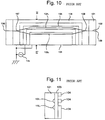
- Fig. 10 and Fig. 11 are figures showing configuration of a Mach-Zehnder light modulator as an example of a waveguide-type device using such electro-optic effects.
- Fig. 10 is a plan view of the Mach-Zehnder light modulator and Fig. 11 is a cross section view taken on line II-II' of Fig. 10.
- the Mach-Zehnder light modulator comprises the base 101 having an electro-optic effect, the light waveguide 102 formed on this base 101, the buffer layer 103 formed on the base 101 and the signal electrode 104 formed on this buffer layer 103.
- the base 101 for example, lithium niobate (LiNbO3) is used frequently.
- the light waveguide 102 is formed by thermally diffusing titanium into the LiNbO3 forming the base.
- a film made of silicon dioxide (SiO2) is used frequently for the buffer layer 103, also gold (Au) is used frequently for the signal electrode 104.
- the signal source for modulation 105 is connected with the signal electrode 104.
- the incident laser light is divided into the light waveguides 1021 and 1022 at the light divergence section 107.
- a phase difference between the light propagating in the light waveguide 1021 and the light propagating in the light waveguide 1022 is caused by an electro-optic effect.
- the light signal of which light strength alternately changes from maximum value and to minimum value is obtained at the light outgoing terminal 109.
- a traveling-wave-type electrode is used for such a light modulator to realize band widening or very high speed.
- this is a configuration that the micro wave modulation voltage is entered from an end of the signal electrode 104 that is a side of light entry and another end of the signal electrode is terminated using impedance of a signal line.
- the light modulation band ⁇ f is dependent on the length l of signal electrode and the transmission refractive index n m of the micro wave.
- n m the transmission refractive index of the micro wave.
- the light modulation band ⁇ f (upper limit of a high speed modulation frequency) is limited by a difference between n m and n, that is, the closer
- the refractive index n of a light waveguide made by doping titanium on a base of lithium niobate is approximately 2.2. Accordingly, it is expected that the transmission refractive index n m of micro wave is also near by this value.
- the interval G between signal electrodes and the thickness t of the signal electrode that makes the transmission refractive index n m be 2.2 that is, one of two factors must be set firstly to determine the value of another factor.
- the interval G between signal electrodes relates to the driving voltage V ⁇ , the narrower the interval G between signal electrodes, the smaller the driving voltage V ⁇ .
- the narrower interval G between signal electrodes is better. In many cases, the value is set less than 15 ⁇ m. By the reason, if the interval G between signal electrodes is set to 15 ⁇ m, the thickness t of signal electrode is determined as 2 ⁇ m by relation shown in Fig.12.
- the characteristic impedance Z of the signal electrode is decided from the characteristics such as the light modulation band ⁇ f of a light device.
- FIG.13 shows a relation between the characteristic impedance Z and the interval G between signal electrodes.
- FIG.13 shows that if letting the interval G between signal electrodes be 15 ⁇ m and the thickness t of the signal electrode be 12 ⁇ m, the characteristic impedance Z becomes 46 ⁇ .
- the characteristic impedance of a signal source for modulation is, however, 50 ⁇ usually.
- the characteristic refractive index n m is firstly matched to the refractive index of a light waveguide in the conventional design stage for a waveguide-type optical device.
- the impedance of the signal electrode of the obtained optical device is different from the impedance of the signal source for modulation.
- the conventional waveguide-type optical device has been used in a state that the characteristic impedance of the signal electrode and the characteristic impedance of the signal source for modulation does not coincided each other.
- a prior art has problems such as the device can not work fully because un-matching of impedance causes deterioration of modulation band or power reflection at the phase of signal input.
- An object of the present invention is to offer a waveguide-type optical device preventing characteristic deterioration caused by un-matching of impedance if using a signal electrode designed by aiming at only transmission refractive index.
- a waveguide-type optical device comprising an impedance matching means for matching impedance of a side of a control signal source supplying a control signal to control propagation of light waves in an optical waveguide of said waveguide-type optical device and impedance of a side of a signal electrode receiving said control signal, wherein said impedance matching means is provided between said side of the control signal source and said side of the signal electrode.
- said impedance matching means is an impedance conversion circuit comprising resistors connected in T network or ⁇ network.
- said impedance matching means can be formed on a base of said waveguide-type optical device, at this time it is preferable that the impedance matching means is an impedance conversion circuit comprising a pattern wiring of resistors.
- the type of said pattern wiring is T network or ⁇ network.
- said signal electrode can be of a co-planar waveguide structure.
- said waveguide-type optical device comprises: a base; an optical waveguide formed on said base; a buffer layer formed on said base; and a signal electrode formed on said buffer layer.
- said waveguide-type optical device can be applied to an optical modulator.
- a waveguide-type optical device comprising: a base; an optical waveguide formed on said base; a buffer layer formed on said base; a signal electrode formed on said buffer layer; a connector for supplying a control signal controlling light waves propagating in said optical waveguide to said signal electrode; and an impedance matching means for matching impedance of said connector and that of said signal electrode.
- said signal electrode is of a co-planar waveguide structure.
- said impedance matching means is an impedance conversion circuit comprising resistors connected in T network or ⁇ network.
- a waveguide-type optical device comprising: a base; an optical waveguide formed on said base; a buffer layer formed on said base; a signal electrode formed on said buffer layer; a connector for supplying a control signal controlling light waves propagating in said optical waveguide to said signal electrode; and an impedance matching means formed on said base for matching impedance of said connector and that of said signal electrode.
- said signal electrode is of a co-planar waveguide structure.
- said impedance matching means is an impedance conversion circuit formed by configuring resistor patterns in T network or ⁇ network on said base.
- an impedance matching method of a waveguide-type optical device comprising: an impedance matching means provided between a side, of a control signal source supplying a control signal to control propagation of light waves in an optical waveguide of said waveguide-type optical device and a side of a signal electrode being supplied said control signal, wherein said impedance matching means matches impedance of said side of the control signal source and that of said side of the signal electrode.
- the present invention enables to reduce troubles such as deterioration of modulation band or occurrence of power reflection at signal entry.
- the present invention enables to miniaturize a waveguide-type optical device by providing an impedance matching means on a base on which an optical waveguide is formed.
- Fig.1 is an illustration showing a configuration of a waveguide-type device provided with a T network impedance conversion circuit by the present invention.
- Fig.2 is a cross section view taken on line I-I' of Fig.1.
- Fig.3 is an illustration for explaining the T network impedance conversion circuit by the present invention.
- Fig.4 is an illustration showing a configuration of a waveguide-type device provided with a T network impedance conversion circuit by the present invention.
- Fig.5 is an illustration for explaining the ⁇ network impedance conversion circuit by the present invention.
- Fig.6 is an illustration showing a configuration of a waveguide-type device provided with a ⁇ network impedance conversion circuit by the present invention.
- Fig.7 is an illustration showing a configuration of a waveguide-type device provided with a ⁇ network impedance conversion circuit by the present invention.
- Figure 8 is an illustration for explaining other embodiment by the present invention.
- Fig.9 is an illustration for explaining another embodiment by the present invention.
- Fig.10 is an illustration for explanation showing a configuration of a Mach-Zehnder light modulator of prior art.
- Fig.11 is a cross section view taken on Line II-II' of Fig.10.
- Figure 12 is a characteristic figure showing a relation between the interval G between electrodes and the transmission refractive index n m of the waveguide-type optical device.
- FIG.13 is a characteristic figure showing a relation between the interval G between electrodes and the characteristic impedance Z of the waveguide-type optical device.
- the first embodiment is explained.
- Fig.1 is a plan view of the waveguide-type optical device in the first embodiment and Fig.2 is a cross section of the line I-I' in Fig.1.
- a Mach-Zehnder light modulator is used in the first embodiment as an example of the waveguide-type optical device.
- Lithium niobate is used here for the base .
- a Ti film of which thickness is approximately 100 nm is formed on the base 1 by sputtering.
- the light waveguide 2 is formed. It is to be noted that the width of the light waveguide 2 is 5 ⁇ m, the interval between the light divergence section 3 and the light junction section 4 is 50mm and the interval between the light waveguides after diverged is 15 ⁇ m, here.
- the buffer layer 5 is formed in thickness of approximately 1 ⁇ m.
- Cr film of approximately 20 nm and Au film of approximately 150 nm as substrate electrodes (not shown in figures) are formed on the buffer layer 5.
- a resist pattern is formed for obtaining a desired pattern of signal electrode and the signal electrode 6 is formed by gilding.
- gilding work a non-cyan liquid is used and plating is performed for approximately 70 minutes in the conditions that liquid temperature is 65°C and current density is 4mA/cm2. By these conditions, an electrode of which thickness is approximately 13 ⁇ m is obtained.
- a Mach-Zehnder light modulator After completion of gilding, a Mach-Zehnder light modulator can be obtained by separating useless resists with a solvent and removing a substrate electrode locating at the part where a signal electrode is not formed by dry-etching.
- the characteristic impedance Z and transmission refractive index n m of the Mach-Zehnder light modulator prepared by the above procedure are 44 ⁇ , 2.15, respectively.
- an SMA connector of which impedance is 50 ⁇ is used as the connector 7.
- the impedance conversion circuit 8 for matching the characteristic impedance of the signal electrode 6 and the impedance of connector 7 is explained.
- T network conversion circuit There can be a T network conversion circuit or a ⁇ network conversion circuit for the impedance conversion circuit 8, the T network conversion circuit using resistors is explained first.
- Fig.3 is an illustration for explaining a T network conversion circuit.
- R1, R2, R3 are resistors
- Z0 is the impedance of the connector 7
- Z1 is the characteristic impedance of the signal electrode 6
- Zi is the impedance of right side of A
- Zo is the impedance of left side of B.
- the allowance for determination of the values is set in ⁇ 1 ⁇ for Zi to Z0 and Zo to Z1, respectively.
- the impedance conversion circuit 8 is produced by soldering the chip resistors thus calculated on the electrode pad.
- Fig.5 is an illustration for explaining the ⁇ network impedance conversion circuit.
- RA, RB and R3 are resistors
- Z0 is the impedance of the connector 7
- Z1 is the characteristic impedance of the signal electrode 6
- Zi is the impedance of right side of C
- Zo is the impedance of left side of D.
- the resistance values of resistors RA, RB and RC are calculated as below.
- Resistor RA 224 ⁇
- Resistor RB 33 ⁇
- Resistor RA 112 ⁇
- the impedance conversion circuit 8 is produced by soldering the resistors thus calculated on the electrode pad.
- resistors RA, RB and RC are as below, because standardized resistors are used for production.
- Resistor RA 220 ⁇
- Resistor RB 33 ⁇
- Resistor RA 120 ⁇
- the resistance value per unit length is approximately 20 ⁇ /mm and the values of resistors RA, RB and RC are as follows. Table 2 Width of electrode Length of electrode Resistor RA 3.3 ⁇ m 3.00mm Resistor RB 12.0 ⁇ m 1.65mm Resistor RC 6.0 ⁇ m 3.00mm
- Fig.3 shows analysis results of characteristics of an optical device provided with such an impedance Conversion circuit 8.
- the optical device of the embodiment realizes the large light modulation band ⁇ f by the small driving voltage V ⁇ . It is confirmed that the present invention can prevent characteristics deterioration caused by impedance un-matching.
- the impedance conversion circuit 8 is configured with resistors in the above embodiment, but it is possible to configure the impedance conversion circuit 8 with conductances C1, C2 and inductance L.
- the values of conductances C1, C2 and the inductance L are, 1pF, 1pF and 3.3nH, respectively.
- the type is free for the conductance and inductance if they have desired electric characteristics.
- the case of converting the characteristic impedance of the signal electrode from 44 ⁇ to 50 ⁇ is not limited to these values. It is possible to design any impedance conversion circuit corresponding to the impedance to be matched.
- the present invention can be applied to other various types of waveguide-type optical devices, although a Mach-Zehnder light modulator has been used as an example for explanation of the present invention in the above embodiment.
Landscapes
- Physics & Mathematics (AREA)
- Nonlinear Science (AREA)
- Electromagnetism (AREA)
- Chemical & Material Sciences (AREA)
- Engineering & Computer Science (AREA)
- Ceramic Engineering (AREA)
- Crystallography & Structural Chemistry (AREA)
- General Physics & Mathematics (AREA)
- Optics & Photonics (AREA)
- Optical Modulation, Optical Deflection, Nonlinear Optics, Optical Demodulation, Optical Logic Elements (AREA)
Applications Claiming Priority (2)
| Application Number | Priority Date | Filing Date | Title |
|---|---|---|---|
| JP14356093 | 1993-06-15 | ||
| JP143560/93 | 1993-06-15 |
Publications (2)
| Publication Number | Publication Date |
|---|---|
| EP0629892A2 true EP0629892A2 (de) | 1994-12-21 |
| EP0629892A3 EP0629892A3 (de) | 1995-08-09 |
Family
ID=15341583
Family Applications (1)
| Application Number | Title | Priority Date | Filing Date |
|---|---|---|---|
| EP94109074A Withdrawn EP0629892A3 (de) | 1993-06-15 | 1994-06-14 | Optische Vorrichtung vom Wellenleitertyp, und Verfahren zur Impedanzpassung dazu. |
Country Status (2)
| Country | Link |
|---|---|
| US (1) | US5572610A (de) |
| EP (1) | EP0629892A3 (de) |
Cited By (4)
| Publication number | Priority date | Publication date | Assignee | Title |
|---|---|---|---|---|
| WO2000068731A3 (en) * | 1999-05-11 | 2001-03-08 | Jds Uniphase Corp | External optical modulation using non-co-linear compensation networks |
| US6580840B1 (en) | 1999-05-11 | 2003-06-17 | Jds Uniphase Corporation | High efficiency electro-optic modulator with equalized frequency response |
| EP1574894A1 (de) * | 2004-03-11 | 2005-09-14 | Avanex Corporation | System zur Verminderung der elektrischen Anpassungsverluste eines Lithiumniobat-Wanderwellenmodulators mit kleinem Wellenwiderstand |
| CN116804804A (zh) * | 2022-03-23 | 2023-09-26 | 富士通光器件株式会社 | 光器件、光调制器和光通信设备 |
Families Citing this family (6)
| Publication number | Priority date | Publication date | Assignee | Title |
|---|---|---|---|---|
| US6763151B1 (en) | 1999-07-02 | 2004-07-13 | Avanex Corporation | Electro-optic modulators with internal impedance matching |
| JP3851825B2 (ja) * | 2002-02-07 | 2006-11-29 | 富士通株式会社 | 光変調器モジュールおよび光変調器 |
| CA2654977A1 (en) * | 2006-06-14 | 2007-12-21 | Anritsu Corporation | Optical modulator |
| US20090267703A1 (en) * | 2008-04-23 | 2009-10-29 | Andrzej May | Dynamically adaptable impedance matching circuitry between an electro-optical load and a driving source |
| JP4668329B2 (ja) * | 2009-03-31 | 2011-04-13 | 住友大阪セメント株式会社 | 光制御デバイス |
| US8426798B2 (en) * | 2009-08-19 | 2013-04-23 | Jds Uniphase Corporation | Electrical termination circuit for a traveling-wave optoelectronic device |
Family Cites Families (7)
| Publication number | Priority date | Publication date | Assignee | Title |
|---|---|---|---|---|
| GB1585097A (en) * | 1976-06-23 | 1981-02-25 | Post Office | Active filter |
| US5010588A (en) * | 1988-03-10 | 1991-04-23 | Bell Communications Research, Inc. | Ultrawide-bandwidth low-noise optical receiver |
| US5097219A (en) * | 1988-12-15 | 1992-03-17 | Mitsubishi Denki Kabushiki Kaisha | Pll for controlling frequency deviation of a variable frequency oscillator |
| US5208697A (en) * | 1990-03-30 | 1993-05-04 | Hughes Aircraft Company | Microwave frequency range electro-optic modulator with efficient input coupling and smooth wideband frequency response |
| US5138480A (en) * | 1991-08-14 | 1992-08-11 | Hewlett-Packard Company | Traveling wave optical modulator |
| JPH0555013A (ja) * | 1991-08-29 | 1993-03-05 | Nec Corp | チツプ型抵抗減衰器 |
| JPH05258924A (ja) * | 1992-03-13 | 1993-10-08 | Fukushima Nippon Denki Kk | チップ型抵抗器 |
-
1994
- 1994-06-13 US US08/259,056 patent/US5572610A/en not_active Expired - Fee Related
- 1994-06-14 EP EP94109074A patent/EP0629892A3/de not_active Withdrawn
Cited By (6)
| Publication number | Priority date | Publication date | Assignee | Title |
|---|---|---|---|---|
| WO2000068731A3 (en) * | 1999-05-11 | 2001-03-08 | Jds Uniphase Corp | External optical modulation using non-co-linear compensation networks |
| US6483953B1 (en) | 1999-05-11 | 2002-11-19 | Jds Uniphase Corporation | External optical modulation using non-co-linear compensation networks |
| US6580840B1 (en) | 1999-05-11 | 2003-06-17 | Jds Uniphase Corporation | High efficiency electro-optic modulator with equalized frequency response |
| EP1574894A1 (de) * | 2004-03-11 | 2005-09-14 | Avanex Corporation | System zur Verminderung der elektrischen Anpassungsverluste eines Lithiumniobat-Wanderwellenmodulators mit kleinem Wellenwiderstand |
| US7228014B2 (en) | 2004-03-11 | 2007-06-05 | Avanex Corporation | System for reducing the electrical return loss of a lithium niobate traveling wave optical modulator with low characteristic impedance |
| CN116804804A (zh) * | 2022-03-23 | 2023-09-26 | 富士通光器件株式会社 | 光器件、光调制器和光通信设备 |
Also Published As
| Publication number | Publication date |
|---|---|
| US5572610A (en) | 1996-11-05 |
| EP0629892A3 (de) | 1995-08-09 |
Similar Documents
| Publication | Publication Date | Title |
|---|---|---|
| US5214724A (en) | Optical waveguide device with suppressed dc drift | |
| US6522793B1 (en) | Low voltage electro-optic modulator with integrated driver | |
| US5138480A (en) | Traveling wave optical modulator | |
| US5005932A (en) | Electro-optic modulator | |
| US5502780A (en) | Waveguide type optical device | |
| US20090297088A1 (en) | Integrated on-chip inductors and capacitors for improved performance of an optical modulator | |
| EP0629892A2 (de) | Optische Vorrichtung vom Wellenleitertyp, und Verfahren zur Impedanzpassung dazu | |
| US6356673B1 (en) | Low loss coplanar waveguide horn for low drive LiNbO3 modulators | |
| EP0717306A1 (de) | Optische Kontrollvorrichtung vom Wellenleitertyp mit unterdrückter Gleichstromdrift, reduzierter Steuerspannung und Betrieb mit hoher Geschwindigkeit | |
| JP2928129B2 (ja) | 光変調器及びその製造方法 | |
| US5515463A (en) | Multi-branch microwave line for electro-optical devices | |
| JPH1039266A (ja) | 光制御デバイス | |
| JP2016194544A (ja) | 広帯域導波路型光素子 | |
| EP1708018A2 (de) | Optischer Modulator und diesen beinhaltendes Kommunikationssystem | |
| US6226423B1 (en) | Optical waveguide element | |
| US6950218B2 (en) | Optical modulator | |
| JPH04172316A (ja) | 導波型光制御デバイス | |
| JPH0798442A (ja) | 導波路型光デバイス | |
| JP2004219600A (ja) | 光変調用電極および光変調器 | |
| US4652078A (en) | Electro-optical directional coupler with three electrodes and alternating dephasing | |
| JPH01231019A (ja) | 光変調器 | |
| JPH11237593A (ja) | 光変調器 | |
| US4707060A (en) | Broadband infrared electro-optic modulator having a buried microstrip network | |
| JPH0293423A (ja) | 光導波路デバイス | |
| JPH1054961A (ja) | 光制御デバイスおよび光制御装置 |
Legal Events
| Date | Code | Title | Description |
|---|---|---|---|
| PUAI | Public reference made under article 153(3) epc to a published international application that has entered the european phase |
Free format text: ORIGINAL CODE: 0009012 |
|
| AK | Designated contracting states |
Kind code of ref document: A2 Designated state(s): DE FR GB SE |
|
| PUAL | Search report despatched |
Free format text: ORIGINAL CODE: 0009013 |
|
| AK | Designated contracting states |
Kind code of ref document: A3 Designated state(s): DE FR GB SE |
|
| 17P | Request for examination filed |
Effective date: 19950629 |
|
| 17Q | First examination report despatched |
Effective date: 19970804 |
|
| STAA | Information on the status of an ep patent application or granted ep patent |
Free format text: STATUS: THE APPLICATION IS DEEMED TO BE WITHDRAWN |
|
| 18D | Application deemed to be withdrawn |
Effective date: 20000104 |