EP0630085A2 - Dispositif semi-conducteur émetteur de lumière et son procédé de fabrication - Google Patents
Dispositif semi-conducteur émetteur de lumière et son procédé de fabrication Download PDFInfo
- Publication number
- EP0630085A2 EP0630085A2 EP94109322A EP94109322A EP0630085A2 EP 0630085 A2 EP0630085 A2 EP 0630085A2 EP 94109322 A EP94109322 A EP 94109322A EP 94109322 A EP94109322 A EP 94109322A EP 0630085 A2 EP0630085 A2 EP 0630085A2
- Authority
- EP
- European Patent Office
- Prior art keywords
- layer
- shutting
- light
- current
- conductivity type
- Prior art date
- Legal status (The legal status is an assumption and is not a legal conclusion. Google has not performed a legal analysis and makes no representation as to the accuracy of the status listed.)
- Granted
Links
Images


Classifications
-
- H—ELECTRICITY
- H10—SEMICONDUCTOR DEVICES; ELECTRIC SOLID-STATE DEVICES NOT OTHERWISE PROVIDED FOR
- H10H—INORGANIC LIGHT-EMITTING SEMICONDUCTOR DEVICES HAVING POTENTIAL BARRIERS
- H10H20/00—Individual inorganic light-emitting semiconductor devices having potential barriers, e.g. light-emitting diodes [LED]
- H10H20/80—Constructional details
- H10H20/81—Bodies
- H10H20/822—Materials of the light-emitting regions
- H10H20/823—Materials of the light-emitting regions comprising only Group II-VI materials, e.g. ZnO
-
- H—ELECTRICITY
- H01—ELECTRIC ELEMENTS
- H01S—DEVICES USING THE PROCESS OF LIGHT AMPLIFICATION BY STIMULATED EMISSION OF RADIATION [LASER] TO AMPLIFY OR GENERATE LIGHT; DEVICES USING STIMULATED EMISSION OF ELECTROMAGNETIC RADIATION IN WAVE RANGES OTHER THAN OPTICAL
- H01S5/00—Semiconductor lasers
- H01S5/30—Structure or shape of the active region; Materials used for the active region
- H01S5/32—Structure or shape of the active region; Materials used for the active region comprising PN junctions, e.g. hetero- or double- heterostructures
- H01S5/327—Structure or shape of the active region; Materials used for the active region comprising PN junctions, e.g. hetero- or double- heterostructures in AIIBVI compounds, e.g. ZnCdSe-laser
-
- H—ELECTRICITY
- H10—SEMICONDUCTOR DEVICES; ELECTRIC SOLID-STATE DEVICES NOT OTHERWISE PROVIDED FOR
- H10H—INORGANIC LIGHT-EMITTING SEMICONDUCTOR DEVICES HAVING POTENTIAL BARRIERS
- H10H20/00—Individual inorganic light-emitting semiconductor devices having potential barriers, e.g. light-emitting diodes [LED]
- H10H20/80—Constructional details
- H10H20/81—Bodies
- H10H20/816—Bodies having carrier transport control structures, e.g. highly-doped semiconductor layers or current-blocking structures
- H10H20/8162—Current-blocking structures
-
- H—ELECTRICITY
- H01—ELECTRIC ELEMENTS
- H01S—DEVICES USING THE PROCESS OF LIGHT AMPLIFICATION BY STIMULATED EMISSION OF RADIATION [LASER] TO AMPLIFY OR GENERATE LIGHT; DEVICES USING STIMULATED EMISSION OF ELECTROMAGNETIC RADIATION IN WAVE RANGES OTHER THAN OPTICAL
- H01S5/00—Semiconductor lasers
- H01S5/20—Structure or shape of the semiconductor body to guide the optical wave ; Confining structures perpendicular to the optical axis, e.g. index or gain guiding, stripe geometry, broad area lasers, gain tailoring, transverse or lateral reflectors, special cladding structures, MQW barrier reflection layers
- H01S5/22—Structure or shape of the semiconductor body to guide the optical wave ; Confining structures perpendicular to the optical axis, e.g. index or gain guiding, stripe geometry, broad area lasers, gain tailoring, transverse or lateral reflectors, special cladding structures, MQW barrier reflection layers having a ridge or stripe structure
- H01S5/2205—Structure or shape of the semiconductor body to guide the optical wave ; Confining structures perpendicular to the optical axis, e.g. index or gain guiding, stripe geometry, broad area lasers, gain tailoring, transverse or lateral reflectors, special cladding structures, MQW barrier reflection layers having a ridge or stripe structure comprising special burying or current confinement layers
- H01S5/2206—Structure or shape of the semiconductor body to guide the optical wave ; Confining structures perpendicular to the optical axis, e.g. index or gain guiding, stripe geometry, broad area lasers, gain tailoring, transverse or lateral reflectors, special cladding structures, MQW barrier reflection layers having a ridge or stripe structure comprising special burying or current confinement layers based on III-V materials
-
- H—ELECTRICITY
- H01—ELECTRIC ELEMENTS
- H01S—DEVICES USING THE PROCESS OF LIGHT AMPLIFICATION BY STIMULATED EMISSION OF RADIATION [LASER] TO AMPLIFY OR GENERATE LIGHT; DEVICES USING STIMULATED EMISSION OF ELECTROMAGNETIC RADIATION IN WAVE RANGES OTHER THAN OPTICAL
- H01S5/00—Semiconductor lasers
- H01S5/20—Structure or shape of the semiconductor body to guide the optical wave ; Confining structures perpendicular to the optical axis, e.g. index or gain guiding, stripe geometry, broad area lasers, gain tailoring, transverse or lateral reflectors, special cladding structures, MQW barrier reflection layers
- H01S5/22—Structure or shape of the semiconductor body to guide the optical wave ; Confining structures perpendicular to the optical axis, e.g. index or gain guiding, stripe geometry, broad area lasers, gain tailoring, transverse or lateral reflectors, special cladding structures, MQW barrier reflection layers having a ridge or stripe structure
- H01S5/223—Buried stripe structure
- H01S5/2231—Buried stripe structure with inner confining structure only between the active layer and the upper electrode
Definitions
- the present invention relates to a semiconductor light emitting device and its manufacturing method, said light emitting device being used as a semiconductor laser device, as a signal reading and writing light emitting device for use in a compact disk (CD) player and a laser disk (LD) player, as a light emitting device for use in a bar code reader, and as a blue light emitting device (LED) for use in displays of other various electronic apparatuses.
- a semiconductor laser device as a signal reading and writing light emitting device for use in a compact disk (CD) player and a laser disk (LD) player
- LD laser disk
- LED blue light emitting device
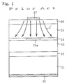
- Fig. 1 shows a blue light emitting semiconductor layer device of ZnSe as an example of a conventional semiconductor light emitting device.
- a group II-VI semiconductor of ZnCdSSe or MgZnCdSSe is grown on an N-type GaAs substrate 21, and a buffer layer 22 made of N-type ZnSe, a light shutting-up layer 23 made of N-type ZnSSe, an active layer 24 made of ZnCdSe, a light shutting-up layer 25 made of P-type ZnSSe and an electrode contact layer 26 made of P-type ZnSe are formed in this order in lamination.
- the light shutting-up layers 23 and 25 made of N-type and P-type ZnSSe, respectively, function to prevent the diffusion of light caused at the active layer 24.
- the light emitting area of the active layer 24 is limited to a belt-shaped central light emitting area 24a, to increase the ratio of the current which contributes to the light emission, it is desirable to limit the spread of the current in a horizontal direction (direction parallel to the active layer 24) to shut up as much current as possible in the central light emitting area 24a of the active layer 24.
- the current is shut up in the following manner: In forming the electrode 27 on the P-type buffer layer 26 which is the electrode contact layer, after a metal is deposited, only a belt-shaped area located opposite the central light emitting area 24a of the active layer 24 is left as the electrode 27 and the other portions are removed by etching, thereby restricting the horizontal spread of the current flowing from the electrode 27 to the active layer 24.
- the ratio of the current which flows through the central light emitting area 24a of the active layer 24 to contribute to the light emission is largely reduced. Consequently, to obtain a necessary current density, a high voltage has to be applied between the electrodes. This not only increases the power consumption but also increases the generation of heat. As a result, the temperature characteristic receives a bad influence.
- the distance between the electrode 27 and the active layer 24 may be decreased by reducing the thickness of the P-type clad layer (light shutting-up layer) 25 and the P-type buffer layer (electrode contact layer) 26 as much as possible.
- the thicknesses of the P-type layers 25 and 26 have to be at least 1 ⁇ m to decrease the influence by the absorption and reflection of light caused at the active layer 24, it is difficult to decrease the distance between the electrode 27 and the active layer 24 under present circumstances.
- the light shutting-up layer 25 shuts up the light travelling in a vertical direction from the electrode 27 toward the active layer 24.
- the horizontal direction there is no difference in refractive index and light absorption since there is only one layer made of only one component, i.e. P-type ZnSSe. Therefore, there is substantially no light guiding path in the horizonal direction, and the guiding of the light in the horizontal direction is made only by shutting up the current. For this reason, to control the angle of spread of light, there is no other way than regulating the distribution of spread of the current. In such a way, however, it is difficult to minutely control the angle of spread of light.
- An object of the present invention is to provide a semiconductor light emitting device and its manufacturing method.
- the power consumption is reduced and the temperature characteristic is improved by increasing the ratio of the current which contributes to the light emission by providing in the light shutting-up layer a structure for preventing the spread of the current, and the light guiding path in the horizontal direction in the light shutting-up layer is minutely controlled.
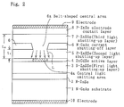
- a group II-VI semiconductor of ZnCdSSe or MgZnCdSSe is grown on a GaAs substrate, and a first light shutting-up layer of the same conductivity type of the conductivity type of the GaAs substrate, an active layer, a second and a third light shutting-up layers of a different conductivity type from the conductivity type of the first light shutting-up layer, and an electrode contact layer are formed in this order in lamination. Electrodes are formed on the outer surfaces of the electrode contact layer and the GaAs substrate.
- a GaAs current shutting-off layer of a different conductivity type from the conductivity type of the second and the third light shutting-up layers is provided on each side of the surface of the second light shutting-up layer so that a belt-shaped central area located opposite a central light emitting area of the active layer is left.
- the current flowing between the electrodes through the active layer flows, at the layer level where the GaAs current shutting-off layer is formed, only through the belt-shaped central area where no current shutting-off layer is formed. Therefore, the current flows in concentration through the central light emitting area of the active layer which is located opposite the belt-shaped central area mentioned above. Further, since the GaAs current shutting-off layer and the active layer are much closer to each other than in the conventional device, the spread of the current is restrained greatly, so that most of the current contributes the light emission.
- the semiconductor light emitting device is manufactured by the following method: First, a group II-VI semiconductor of ZnCdSSe or MgZnCdSSe is grown on the GaAs substrate to form the first light shutting-up layer of the same conductivity type as the conductivity type of the GaAs substrate, the active layer, and the second light shutting-up layer of a different conductivity type of the conductivity type of the first light shutting-up layer in this order in lamination. Then, on the entire surface of the second light shutting-up layer, GaAs of a different conductivity type from the conductivity type of the second light shutting-up layer is grown to form a GaAs layer.
Landscapes
- Physics & Mathematics (AREA)
- Condensed Matter Physics & Semiconductors (AREA)
- General Physics & Mathematics (AREA)
- Electromagnetism (AREA)
- Optics & Photonics (AREA)
- Led Devices (AREA)
- Semiconductor Lasers (AREA)
Applications Claiming Priority (3)
| Application Number | Priority Date | Filing Date | Title |
|---|---|---|---|
| JP14584493A JPH077183A (ja) | 1993-06-17 | 1993-06-17 | 半導体発光装置及びその製造方法 |
| JP145844/93 | 1993-06-17 | ||
| JP14584493 | 1993-06-17 |
Publications (3)
| Publication Number | Publication Date |
|---|---|
| EP0630085A2 true EP0630085A2 (fr) | 1994-12-21 |
| EP0630085A3 EP0630085A3 (fr) | 1998-04-08 |
| EP0630085B1 EP0630085B1 (fr) | 2001-10-10 |
Family
ID=15394413
Family Applications (1)
| Application Number | Title | Priority Date | Filing Date |
|---|---|---|---|
| EP94109322A Expired - Lifetime EP0630085B1 (fr) | 1993-06-17 | 1994-06-16 | Dispositif semi-conducteur II-VI émetteur de lumière et son procédé de fabrication |
Country Status (4)
| Country | Link |
|---|---|
| US (1) | US5477063A (fr) |
| EP (1) | EP0630085B1 (fr) |
| JP (1) | JPH077183A (fr) |
| DE (1) | DE69428556T2 (fr) |
Cited By (2)
| Publication number | Priority date | Publication date | Assignee | Title |
|---|---|---|---|---|
| DE29511927U1 (de) * | 1995-07-24 | 1997-01-09 | THERA Patent GmbH & Co. KG Gesellschaft für industrielle Schutzrechte, 82229 Seefeld | Lichtpolymerisationsgerät |
| CN116978999A (zh) * | 2023-09-22 | 2023-10-31 | 南昌凯捷半导体科技有限公司 | 一种电流限域Micro-LED芯片及其制作方法 |
Families Citing this family (13)
| Publication number | Priority date | Publication date | Assignee | Title |
|---|---|---|---|---|
| US6996150B1 (en) | 1994-09-14 | 2006-02-07 | Rohm Co., Ltd. | Semiconductor light emitting device and manufacturing method therefor |
| US5924002A (en) * | 1994-12-22 | 1999-07-13 | Sony Corporation | Method of manufacturing a semiconductor device having ohmic electrode |
| DE69625384T2 (de) * | 1995-01-20 | 2003-04-17 | Matsushita Electric Industrial Co., Ltd. | Lichtemittierende Halbleitervorrichtung und Herstellungsverfahren |
| US5742629A (en) * | 1995-07-21 | 1998-04-21 | Matsushita Electric Industrial Co., Ltd. | Semiconductor laser and production method thereof |
| JPH0997943A (ja) * | 1995-09-28 | 1997-04-08 | Denso Corp | スタック型半導体レーザ |
| JP2930032B2 (ja) * | 1996-09-26 | 1999-08-03 | 日本電気株式会社 | Ii−vi族化合物半導体発光素子およびその製造方法 |
| US5732103A (en) * | 1996-12-09 | 1998-03-24 | Motorola, Inc. | Long wavelength VCSEL |
| US6023483A (en) * | 1997-03-26 | 2000-02-08 | Mitsubishi Chemical Corporation | Semiconductor light-emitting device |
| US5963573A (en) * | 1997-08-25 | 1999-10-05 | 3M Innovative Properties Company | Light absorbing layer for II-VI semiconductor light emitting devices |
| US7304325B2 (en) * | 2000-05-01 | 2007-12-04 | Toyoda Gosei Co., Ltd. | Group III nitride compound semiconductor light-emitting device |
| US6429460B1 (en) * | 2000-09-28 | 2002-08-06 | United Epitaxy Company, Ltd. | Highly luminous light emitting device |
| CN101459209B (zh) * | 2007-12-14 | 2012-04-18 | 台达电子工业股份有限公司 | 发光二极管装置及其制造方法 |
| KR20210156624A (ko) * | 2020-06-18 | 2021-12-27 | 삼성전자주식회사 | 나노 막대 발광 소자 및 그 제조 방법 |
Family Cites Families (9)
| Publication number | Priority date | Publication date | Assignee | Title |
|---|---|---|---|---|
| DE3065856D1 (en) * | 1979-02-13 | 1984-01-19 | Fujitsu Ltd | A semiconductor light emitting device |
| JPS55123191A (en) * | 1979-03-16 | 1980-09-22 | Fujitsu Ltd | Semiconductor light emitting device |
| JPS566480A (en) * | 1979-06-27 | 1981-01-23 | Fujitsu Ltd | Semiconductor light emitting diode |
| JPS58127393A (ja) * | 1982-01-25 | 1983-07-29 | Mitsubishi Electric Corp | 半導体レ−ザ装置の製造方法 |
| JPH03244118A (ja) * | 1990-02-22 | 1991-10-30 | Sumitomo Electric Ind Ltd | 化合物半導体基板の製造方法 |
| JPH03292778A (ja) * | 1990-04-10 | 1991-12-24 | Nec Corp | 半導体発光素子 |
| DE69218683T2 (de) * | 1991-07-15 | 1997-11-13 | Sony Corp | Halbleiterlaser |
| JPH0590706A (ja) * | 1991-09-26 | 1993-04-09 | Anritsu Corp | 半導体レーザ素子 |
| JPH05291619A (ja) * | 1992-04-13 | 1993-11-05 | Toshiba Corp | 半導体素子 |
-
1993
- 1993-06-17 JP JP14584493A patent/JPH077183A/ja active Pending
-
1994
- 1994-06-15 US US08/260,982 patent/US5477063A/en not_active Expired - Fee Related
- 1994-06-16 DE DE69428556T patent/DE69428556T2/de not_active Expired - Fee Related
- 1994-06-16 EP EP94109322A patent/EP0630085B1/fr not_active Expired - Lifetime
Cited By (3)
| Publication number | Priority date | Publication date | Assignee | Title |
|---|---|---|---|---|
| DE29511927U1 (de) * | 1995-07-24 | 1997-01-09 | THERA Patent GmbH & Co. KG Gesellschaft für industrielle Schutzrechte, 82229 Seefeld | Lichtpolymerisationsgerät |
| CN116978999A (zh) * | 2023-09-22 | 2023-10-31 | 南昌凯捷半导体科技有限公司 | 一种电流限域Micro-LED芯片及其制作方法 |
| CN116978999B (zh) * | 2023-09-22 | 2024-01-02 | 南昌凯捷半导体科技有限公司 | 一种电流限域Micro-LED芯片及其制作方法 |
Also Published As
| Publication number | Publication date |
|---|---|
| DE69428556D1 (de) | 2001-11-15 |
| EP0630085A3 (fr) | 1998-04-08 |
| US5477063A (en) | 1995-12-19 |
| DE69428556T2 (de) | 2002-06-13 |
| EP0630085B1 (fr) | 2001-10-10 |
| JPH077183A (ja) | 1995-01-10 |
Similar Documents
| Publication | Publication Date | Title |
|---|---|---|
| EP0630085B1 (fr) | Dispositif semi-conducteur II-VI émetteur de lumière et son procédé de fabrication | |
| EP0132081B1 (fr) | Laser à semi-conducteur | |
| EP0103415A2 (fr) | Dispositifs émetteurs de lumière et leurs procédés de fabrication | |
| US5177757A (en) | Semiconductor laser producing visible light | |
| EP0806823B1 (fr) | Laser à semi-conducteur ayant un substrat écheloné pour émission de lumière d'une partie en pente | |
| US4810670A (en) | Method of manufacturing an embedded type semiconductor laser | |
| US4855250A (en) | Method of manufacturing a semiconductor laser with autodoping control | |
| US6154476A (en) | Semiconductor laser diode | |
| EP0500351A2 (fr) | Laser à semi-conducteur | |
| US5521396A (en) | Semiconductor light emitting device | |
| US5548127A (en) | Semiconductor light emitting device and its manufacturing method | |
| EP0000267B1 (fr) | Source de lumière dans un système optique de communication | |
| EP0260110A2 (fr) | Diode électroluminescente à double hétérostructure | |
| US20040224434A1 (en) | Method of forming a semiconductor structure for use in a light emitting diode and a semiconductor structure | |
| US5567960A (en) | II/VI-compound semiconductor light emitting device | |
| US5192711A (en) | Method for producing a semiconductor laser device | |
| US4926432A (en) | Semiconductor laser device | |
| US4359775A (en) | Semiconductor laser | |
| CA1179049A (fr) | Laser a semiconducteur | |
| JPH06350200A (ja) | 半導体発光装置及びその製造方法 | |
| JPS6133275B2 (fr) | ||
| JP3288481B2 (ja) | 半導体発光装置の製造方法 | |
| KR100408531B1 (ko) | GaN계 레이저 다이오드 | |
| JPH03203282A (ja) | 半導体レーザダイオード | |
| JPH06350199A (ja) | 半導体発光装置及びその製造方法 |
Legal Events
| Date | Code | Title | Description |
|---|---|---|---|
| PUAI | Public reference made under article 153(3) epc to a published international application that has entered the european phase |
Free format text: ORIGINAL CODE: 0009012 |
|
| AK | Designated contracting states |
Kind code of ref document: A2 Designated state(s): DE FR GB |
|
| PUAL | Search report despatched |
Free format text: ORIGINAL CODE: 0009013 |
|
| AK | Designated contracting states |
Kind code of ref document: A3 Designated state(s): DE FR GB |
|
| 17P | Request for examination filed |
Effective date: 19980602 |
|
| 17Q | First examination report despatched |
Effective date: 19991102 |
|
| RIC1 | Information provided on ipc code assigned before grant |
Free format text: 7H 01S 5/32 A, 7H 01L 33/00 B |
|
| RTI1 | Title (correction) |
Free format text: II-VI SEMICONDUCTOR LIGHT EMITTING DEVICE AND ITS MANUFACTURING METHOD |
|
| GRAG | Despatch of communication of intention to grant |
Free format text: ORIGINAL CODE: EPIDOS AGRA |
|
| GRAH | Despatch of communication of intention to grant a patent |
Free format text: ORIGINAL CODE: EPIDOS IGRA |
|
| GRAH | Despatch of communication of intention to grant a patent |
Free format text: ORIGINAL CODE: EPIDOS IGRA |
|
| GRAA | (expected) grant |
Free format text: ORIGINAL CODE: 0009210 |
|
| AK | Designated contracting states |
Kind code of ref document: B1 Designated state(s): DE FR GB |
|
| PG25 | Lapsed in a contracting state [announced via postgrant information from national office to epo] |
Ref country code: FR Free format text: LAPSE BECAUSE OF FAILURE TO SUBMIT A TRANSLATION OF THE DESCRIPTION OR TO PAY THE FEE WITHIN THE PRESCRIBED TIME-LIMIT Effective date: 20011010 |
|
| REF | Corresponds to: |
Ref document number: 69428556 Country of ref document: DE Date of ref document: 20011115 |
|
| REG | Reference to a national code |
Ref country code: GB Ref legal event code: IF02 |
|
| PG25 | Lapsed in a contracting state [announced via postgrant information from national office to epo] |
Ref country code: GB Free format text: LAPSE BECAUSE OF NON-PAYMENT OF DUE FEES Effective date: 20020616 |
|
| EN | Fr: translation not filed | ||
| PLBE | No opposition filed within time limit |
Free format text: ORIGINAL CODE: 0009261 |
|
| STAA | Information on the status of an ep patent application or granted ep patent |
Free format text: STATUS: NO OPPOSITION FILED WITHIN TIME LIMIT |
|
| 26N | No opposition filed | ||
| GBPC | Gb: european patent ceased through non-payment of renewal fee |
Effective date: 20020616 |
|
| PGFP | Annual fee paid to national office [announced via postgrant information from national office to epo] |
Ref country code: DE Payment date: 20030626 Year of fee payment: 10 |
|
| PG25 | Lapsed in a contracting state [announced via postgrant information from national office to epo] |
Ref country code: DE Free format text: LAPSE BECAUSE OF NON-PAYMENT OF DUE FEES Effective date: 20050101 |