EP0631312A1 - Boîtier avec plots de contact alignés - Google Patents
Boîtier avec plots de contact alignés Download PDFInfo
- Publication number
- EP0631312A1 EP0631312A1 EP94104613A EP94104613A EP0631312A1 EP 0631312 A1 EP0631312 A1 EP 0631312A1 EP 94104613 A EP94104613 A EP 94104613A EP 94104613 A EP94104613 A EP 94104613A EP 0631312 A1 EP0631312 A1 EP 0631312A1
- Authority
- EP
- European Patent Office
- Prior art keywords
- semiconductor device
- circuit board
- wiring lines
- edges
- boards
- Prior art date
- Legal status (The legal status is an assumption and is not a legal conclusion. Google has not performed a legal analysis and makes no representation as to the accuracy of the status listed.)
- Granted
Links
Images






Classifications
-
- H—ELECTRICITY
- H05—ELECTRIC TECHNIQUES NOT OTHERWISE PROVIDED FOR
- H05K—PRINTED CIRCUITS; CASINGS OR CONSTRUCTIONAL DETAILS OF ELECTRIC APPARATUS; MANUFACTURE OF ASSEMBLAGES OF ELECTRICAL COMPONENTS
- H05K3/00—Apparatus or processes for manufacturing printed circuits
- H05K3/30—Assembling printed circuits with electric components, e.g. with resistors
- H05K3/303—Assembling printed circuits with electric components, e.g. with resistors with surface mounted components
-
- H—ELECTRICITY
- H10—SEMICONDUCTOR DEVICES; ELECTRIC SOLID-STATE DEVICES NOT OTHERWISE PROVIDED FOR
- H10W—GENERIC PACKAGES, INTERCONNECTIONS, CONNECTORS OR OTHER CONSTRUCTIONAL DETAILS OF DEVICES COVERED BY CLASS H10
- H10W70/00—Package substrates; Interposers; Redistribution layers [RDL]
- H10W70/60—Insulating or insulated package substrates; Interposers; Redistribution layers
- H10W70/62—Insulating or insulated package substrates; Interposers; Redistribution layers characterised by their interconnections
- H10W70/65—Shapes or dispositions of interconnections
-
- H—ELECTRICITY
- H10—SEMICONDUCTOR DEVICES; ELECTRIC SOLID-STATE DEVICES NOT OTHERWISE PROVIDED FOR
- H10W—GENERIC PACKAGES, INTERCONNECTIONS, CONNECTORS OR OTHER CONSTRUCTIONAL DETAILS OF DEVICES COVERED BY CLASS H10
- H10W90/00—Package configurations
- H10W90/401—Package configurations characterised by multiple insulating or insulated package substrates, interposers or RDLs
-
- H—ELECTRICITY
- H10—SEMICONDUCTOR DEVICES; ELECTRIC SOLID-STATE DEVICES NOT OTHERWISE PROVIDED FOR
- H10W—GENERIC PACKAGES, INTERCONNECTIONS, CONNECTORS OR OTHER CONSTRUCTIONAL DETAILS OF DEVICES COVERED BY CLASS H10
- H10W90/00—Package configurations
- H10W90/701—Package configurations characterised by the relative positions of pads or connectors relative to package parts
-
- H—ELECTRICITY
- H05—ELECTRIC TECHNIQUES NOT OTHERWISE PROVIDED FOR
- H05K—PRINTED CIRCUITS; CASINGS OR CONSTRUCTIONAL DETAILS OF ELECTRIC APPARATUS; MANUFACTURE OF ASSEMBLAGES OF ELECTRICAL COMPONENTS
- H05K2201/00—Indexing scheme relating to printed circuits covered by H05K1/00
- H05K2201/09—Shape and layout
- H05K2201/09209—Shape and layout details of conductors
- H05K2201/09654—Shape and layout details of conductors covering at least two types of conductors provided for in H05K2201/09218 - H05K2201/095
- H05K2201/09781—Dummy conductors, i.e. not used for normal transport of current; Dummy electrodes of components
-
- H—ELECTRICITY
- H05—ELECTRIC TECHNIQUES NOT OTHERWISE PROVIDED FOR
- H05K—PRINTED CIRCUITS; CASINGS OR CONSTRUCTIONAL DETAILS OF ELECTRIC APPARATUS; MANUFACTURE OF ASSEMBLAGES OF ELECTRICAL COMPONENTS
- H05K2201/00—Indexing scheme relating to printed circuits covered by H05K1/00
- H05K2201/10—Details of components or other objects attached to or integrated in a printed circuit board
- H05K2201/10431—Details of mounted components
- H05K2201/10439—Position of a single component
- H05K2201/10454—Vertically mounted
-
- H—ELECTRICITY
- H05—ELECTRIC TECHNIQUES NOT OTHERWISE PROVIDED FOR
- H05K—PRINTED CIRCUITS; CASINGS OR CONSTRUCTIONAL DETAILS OF ELECTRIC APPARATUS; MANUFACTURE OF ASSEMBLAGES OF ELECTRICAL COMPONENTS
- H05K2201/00—Indexing scheme relating to printed circuits covered by H05K1/00
- H05K2201/10—Details of components or other objects attached to or integrated in a printed circuit board
- H05K2201/10431—Details of mounted components
- H05K2201/10568—Integral adaptations of a component or an auxiliary PCB for mounting, e.g. integral spacer element
-
- H—ELECTRICITY
- H05—ELECTRIC TECHNIQUES NOT OTHERWISE PROVIDED FOR
- H05K—PRINTED CIRCUITS; CASINGS OR CONSTRUCTIONAL DETAILS OF ELECTRIC APPARATUS; MANUFACTURE OF ASSEMBLAGES OF ELECTRICAL COMPONENTS
- H05K2201/00—Indexing scheme relating to printed circuits covered by H05K1/00
- H05K2201/10—Details of components or other objects attached to or integrated in a printed circuit board
- H05K2201/10613—Details of electrical connections of non-printed components, e.g. special leads
- H05K2201/10621—Components characterised by their electrical contacts
- H05K2201/10659—Different types of terminals for the same component, e.g. solder balls combined with leads
-
- H—ELECTRICITY
- H05—ELECTRIC TECHNIQUES NOT OTHERWISE PROVIDED FOR
- H05K—PRINTED CIRCUITS; CASINGS OR CONSTRUCTIONAL DETAILS OF ELECTRIC APPARATUS; MANUFACTURE OF ASSEMBLAGES OF ELECTRICAL COMPONENTS
- H05K2201/00—Indexing scheme relating to printed circuits covered by H05K1/00
- H05K2201/10—Details of components or other objects attached to or integrated in a printed circuit board
- H05K2201/10613—Details of electrical connections of non-printed components, e.g. special leads
- H05K2201/10621—Components characterised by their electrical contacts
- H05K2201/10696—Single-in-line [SIL] package
-
- H—ELECTRICITY
- H05—ELECTRIC TECHNIQUES NOT OTHERWISE PROVIDED FOR
- H05K—PRINTED CIRCUITS; CASINGS OR CONSTRUCTIONAL DETAILS OF ELECTRIC APPARATUS; MANUFACTURE OF ASSEMBLAGES OF ELECTRICAL COMPONENTS
- H05K3/00—Apparatus or processes for manufacturing printed circuits
- H05K3/30—Assembling printed circuits with electric components, e.g. with resistors
- H05K3/32—Assembling printed circuits with electric components, e.g. with resistors electrically connecting electric components or wires to printed circuits
- H05K3/34—Assembling printed circuits with electric components, e.g. with resistors electrically connecting electric components or wires to printed circuits by soldering
- H05K3/341—Surface mounted components
- H05K3/3421—Leaded components
- H05K3/3426—Leaded components characterised by the leads
-
- Y—GENERAL TAGGING OF NEW TECHNOLOGICAL DEVELOPMENTS; GENERAL TAGGING OF CROSS-SECTIONAL TECHNOLOGIES SPANNING OVER SEVERAL SECTIONS OF THE IPC; TECHNICAL SUBJECTS COVERED BY FORMER USPC CROSS-REFERENCE ART COLLECTIONS [XRACs] AND DIGESTS
- Y02—TECHNOLOGIES OR APPLICATIONS FOR MITIGATION OR ADAPTATION AGAINST CLIMATE CHANGE
- Y02P—CLIMATE CHANGE MITIGATION TECHNOLOGIES IN THE PRODUCTION OR PROCESSING OF GOODS
- Y02P70/00—Climate change mitigation technologies in the production process for final industrial or consumer products
- Y02P70/50—Manufacturing or production processes characterised by the final manufactured product
Definitions
- This invention generally relates to semiconductor devices, and more particularly to a semiconductor device which can be mounted on a circuit board so that the semiconductor device stands vertically.
- a surface mounting package has been widely used in which a semiconductor device is soldered on a circuit board, rather than holes made to the circuit board and used to solder leads thereon.
- a package placed vertically on the mounting surface of the circuit board (hereinafter referred to as a "vertical package") is known in order to increase the density of mounting on the circuit board.
- FIG. 1 shows a semiconductor device 1 disclosed in the above application.
- a resin package 2 houses a semiconductor device 3.
- Inner lead portions 4a of leads 4 are connected with the semiconductor device 3, and the outer lead portions 4b thereof extend out of the package 2. Further, predetermined tip portions of the outer leads 4b are bent at the same angle.
- Spacers 5 are placed on both ends of the section from which the outer leads 4b of the package 2 extend.
- Each of the spacers 5 includes a clip 6 and a cylinder part 7 with the diameter contractible.
- the spacers 5 are used, as shown in Fig. 2, to mount the semiconductor device 1 on a circuit board 8.
- Slots 8a with which the relevant cylinder parts 7 can be engaged are formed on the circuit board 8.
- the semiconductor device 1 is made to stand vertically on the circuit board 8 by engaging the cylinder parts 7 with the slots 8a of the spacers 5.
- the outer leads 4b are soldered to a pattern 8b formed on the circuit board 8.
- the slots 8a are needed to vertically place the semiconductor packages 1 on the circuit board 8.
- the holes 8a have to be formed before mounting. This is a problem because it reduces mounting efficiency.
- the outer lead 4b extends for a relatively long distance toward the circuit board 8 and is bent.
- the bent portion of the outer leads 4b is soldered to the pattern 8b formed on the circuit board 8. That is, the outer lead 4b has a long portion extending out of package 2. External disturbances may enter through this exposed portion, which may prevent favorable transmission of signals between the semiconductor device 1 and the circuit board 8.
- the applicant has proposed, as set forth in Japanese Laid-Open Patent Application No. 4-52434, a semiconductor device with a structure in which a resin package is placed vertically on a circuit board and connection leads are bent in the vicinity of the resin package in order to support the resin package with supporting leads extended in opposite directions from each other.
- a more specific object of the present invention is to provide a multiple-pin semiconductor device which can be mounted on a small circuit board and contributes to down-sizing of electronic devices.
- a semiconductor device comprising: vertical placement means for mounting the semiconductor device on a surface of a circuit board in a vertical position; connection means for making electrical connections between the circuit board and a semiconductor element; a stage on which the semiconductor element is placed, the stage having supporting members causing the semiconductor device to vertically stand on the circuit board; and wiring boards stacked on a side of the stage on which the semiconductor element is placed, the wiring boards having windows in which the semiconductor element is located.
- the vertical placement means comprises wiring lines extending between edges of the circuit boards facing the circuit board and peripheries of the windows. The wiring lines have ends located in the vicinity of the edges of the circuit boards and have a shape enabling the semiconductor device to be mounted on the circuit board.
- Fig. 3 is a perspective view of the whole of the first embodiment of the invention.
- Fig. 4 is an enlarged, perspective view of a part of the first embodiment of the invention.
- a semiconductor device 10 is of a vertical structure, and has supporting members 12a, 12b, 12c, and 12d bent into an L-shape to enable vertical mounting of the semiconductor device 10 on the mounting surface of a circuit board 11.
- the semiconductor device 10 comprises a metallic stage 15, a metallic plate 16, and single-layered printed wiring boards 17 and 18 in a stacked configuration.
- the supporting members 12a and 12c are formed as a single unit with the metallic stage 15, and the supporting members 12b and 12d are formed as a single unit with the metallic plate 16.
- a semiconductor element (chip) 13 is placed in the central position on the surface of the metallic stage 15.
- a window 22 is created in the metallic plate 16 and the printed wiring boards 17 and 18, and is located in a position corresponding to the position of the semiconductor element 13.
- printed wiring lines (interconnections) 14 are formed, which extend from the periphery of the window 22 to edges 20 and 21 of the boards 17 and 18 facing the circuit board 11.
- each of the wiring lines 14 is wire-bonded to the semiconductor element 13 by a bonding wire (not shown).
- the other ends of the wiring lines 14 have L-shaped portions which are located in the vicinity of the edges 20 and 21 of the printed wiring boards 17 and 18 facing the circuit board 11 and which extend in opposite directions along with the supporting members.
- the above structure enables flexible mounting on the mounting surface of the circuit board 11.
- the semiconductor element 13 is sealed by resin potting.
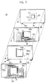
- Fig. 5 is an exploded perspective view of the first embodiment of the invention
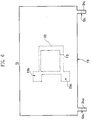
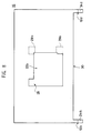
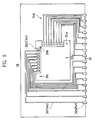
- Figs. 6 through 9 are plan views of the metallic stage 15, the printed wiring board 17, the metallic plate 16, and the circuit board 11, respectively.
- the metallic stage 15, on which semiconductor element 13 is mounted is of an approximately rectangular shape.
- the supporting members 12a and 12c project from the long edge 19 of the metallic stage 15 facing the circuit board 11.
- the supporting members 12a and 12c are bent into L-shapes in the position indicated by a dotted line.
- the supporting members 12a and 12c respectively have contact surfaces 24a and 24c, which come into contact with the circuit board 11.
- the mounting area 23 formed on the center surface portion of the metallic stage 15 is plated with palladium (Pd), gold (Ag) or silver (Au). Accordingly, the semiconductor element 13 can be mounted and wire-bonded on the mounting area 23.
- the printed wiring board 17, stacked on the front surface of the metallic stage 15, is nearly rectangular, with a window 22a formed in the middle of its surface. Areas 25a, 25b and 25c are cut out of three corners of the window 22a, which is nearly square in shape.
- the printed circuit board 17 is structured so that, when it is stacked onto the metallic stage 15, extensions 23a and 23b of the mounting area 23 on the metallic stage 15 can be seen through the cutout sections 25b and 25c, respectively.
- a plurality of conductor pads 26a are aligned along the left edge of the window 22a.
- the conductor pads 26a are connected via intermediate patterns 27 to conductor pads 26b arranged in a line along the long edge 20, which faces the circuit board 11.
- the conductor pads 26a and 26b and the intermediate patterns 27 form the printed wiring lines 14a.
- the printed wiring lines 14b are formed to extend between the lower edge of the window 22a and the edge 20, which faces the circuit board 11.
- the printed wiring lines 14b As compared to other printed wiring lines (printed wiring lines 14a, and printed wiring lines 14c and 14d which will be described later), the printed wiring lines 14b have the shortest path. Hence, the printed wiring lines 14b are used for signals required to be transferred with the fastest response.
- the metallic plate 16 stacked on the main surface side of the printed circuit board 17 (on which the printed wiring lines are formed) is of an approximately rectangular shape, and a window 22b is formed in the metallic plate 16 and is located in the center surface portion thereof.
- the window 22b is of a nearly square shape, and has a cutout portion 28 formed in one corner thereof.
- the window 22b has two mounting portions 29a and 29b formed in the vicinity of two other corners.
- the mounting portions 29a and 29b are plated with palladium (Pd), gold (Ag), copper (Au) or other metallic materials, so that wire bonding is possible.
- the supporting members 12b and 12d project from the two corners of the long edge 30 of the metallic plate 16 that faces the circuit board 11 and are bent in an L-shape in the position indicated by a broken line. Hence, the supporting members 12b and 12d respectively have contact surfaces, which come into contact with the circuit board 11.
- the supporting members 12b and 12d are formed so that when the metallic plate 16, the printed wiring board 17, and the metallic stage 15 are stacked, the supporting members 12b and 12d are located in positions different from those of the supporting members 12a and 12d of the metallic stage 15.
- the window 22b is formed so that the mounting area 23 of the metallic stage 15, the conductor pads 26a in the printed wiring lines 14a on the printed wiring board 17, and the conductor pads 26c of the printed wiring lines 14b on the printed wiring board 17 can be seen through the window 22b.
- the printed wiring board 18, which is stacked on the front surface of the metallic plate 16 is of a nearly rectangular shape.
- a window 22c is formed in the metallic plate 16 and is located in the center surface portion thereof.
- the window 22c is of a nearly square shape, and has cutout portions 31a, 31b, and 31c respectively formed in the three corners of the window 22c.
- the window 22b is formed so that the extensions 23a and 23b of the mounting area 23 of the metallic stage 15, the conductor pads 26a of printed wiring lines 14a of the printed circuit board 17, and the conductor pads 26c of the printed wiring lines 14b thereof can be seen through the window 22c.
- a plurality of conductor pads 32a are aligned along the upper edge of the window 22c.
- the conductor pads 32a are connected via intermediate patterns 33 to conductor pads 32b which are aligned along the long edge 21 of the printed wiring board 18 and face the circuit board 11.
- the conductor pads 32a and 32b and the intermediate patterns 33 form the printed wiring lines 14c.
- printed wiring lines 14d are formed so that they extend from the right edge of the window 22c to the edge 21 of the printed wiring board 18.
- the printed wiring lines 14c and 14d along the edge 21 of the printed wiring board 18 are located in a zigzag (staggered) manner with respect to the printed wiring lines 14a and 14b of the printed wiring board 17. Further, the end portions of the printed wiring lines 14a, 14b, 14c and 14d are bent into L-shapes so that the lines 14c and 14d extend in the direction opposite to the direction in which the lines 14a and 14b extend.
- the metallic stage 15, the printed wiring board 17, the metallic plate 16, and the printed wiring board 18 are stacked in that order as shown in Fig. 10, which provides a plain view of the semiconductor device 10.
- the semiconductor device 10 has the vertical structure in which the device 10 is vertically mounted on the mounting surface of the circuit board 11 and the printed wiring lines are arranged in two lines in zigzag form.
- the semiconductor device 10 can be mounted on a compact circuit board.
- the use of single-layered printed wiring boards reduces material costs and facilitates the formation of printed wiring lines, so that the production cost can be reduced.
- the metallic stage 15 forms the back surface of the semiconductor device 10, so that heat generated by the semiconductor element 13 can be effectively and efficiently radiated.
- the metallic stage and the metallic plate are plated to be stacked in a bondable state, they serve as a low-impedance grounding layer or power supply layer and thus contribute to improvements in the electrical characteristics.
- Fig. 11 is a perspective view of an essential part of a variation of the first embodiment of the present invention.
- a semiconductor device 35 shown in Fig. 11 has printed wiring lines 14c having cylindrical ends located in the vicinity of the edges 20 and 30 facing the circuit board 11.
- the contact surfaces of the printed circuit lines 14e that come into contact with the circuit board 11 are of a nearly circular shape.
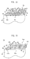
- Fig. 12 is a perspective view of the whole of the second embodiment of the invention.
- Fig. 13 is an enlarged, perspective view of a part of the second embodiment of the invention.
- Fig. 14 is an exploded, perspective view of the second embodiment of the present invention. The second embodiment of the present invention will be described with reference to Figs. 12 through 14.
- a semiconductor device 40 according to the third embodiment of the present invention has a vertical structure and is supported by supporting members 42a, 42b, 42c, and 42d, each of which members is bent in an L-shape.
- the semiconductor device 40 is vertically mounted on the mounting surface of the circuit board 11.
- the semiconductor device 40 includes a metallic stage 45, a single-layer printed circuit board 46, a single-layer printed circuit board 47, a metallic plate 48, a single-layer printed circuit board 49 and a single-layer printed circuit board 50 stacked in this order.
- Supporting members 42a and 42c are integrated with the metallic stage 45, and supporting members 42b and 42d are integrated with the metallic plate 48.
- the semiconductor element 13 is mounted on the center surface portion of the metallic stage 45.
- Windows 62c, 62a, 62b, 62d, and 62e are formed in the metallic plate 48 and the printed wiring boards 46, 47, 49, and 50, and are located at respective positions corresponding to the position of the semiconductor element 13.
- printed wiring lines 64a, 64b, 64c, and 64d which are connection means, are formed so as to extend from the areas around windows 62a, 62b, 62d, and 62e to edges 52, 53, 55, and 56 facing the board 11, respectively.
- One-ends of the printed wiring lines 64a, 64b, 64c, and 64d are wire-bonded to the semiconductor element 13 by means of bonding wires (not shown).
- the other ends of the printed wiring lines 64a, 64b, 64c and 64d are bent in the vicinity of the edges 52, 53, 55 and 56 of the boards 46, 47, 49 and 50 facing the circuit board 11, so that the lines 64a and 64b and the supporting members 42a and 42c extend in the direction opposite to that in which the lines 64c and 64d and the supporting members 42b and 42d extend.
- the above structure enables flexible surface mounting on the mounting surface of the circuit board 11.
- the wire-bonded semiconductor element 13 is sealed by resin potting.
- the semiconductor device 40 includes a mounting portion 63 and contact portions 59a and 59b, on which the semiconductor element 13 can be mounted.
- the portions 63, 59a and 59b are plated with palladium (Pd), gold (Ag), silver (Au), or other metals to allow wire bonding.
- the semiconductor device 40 has the vertical structure in which the device 40 is vertically mounted on the mounting surface of the circuit board 11 and the printed wiring lines are arranged in four lines in double zigzag form.
- the third embodiment of the present invention as compared with the first embodiment of the present invention, it is possible to provide a large number of pins without an increase in the length of the package in the direction in which the pins are arranged and mount the semiconductor device 40 with a mounting length equal to that needed to mount a single in-line package device. Hence, the semiconductor device 40 can be mounted on a compact circuit board. Further, the second embodiment of the present invention has advantages in terms of the production cost, electrical characteristics, and heat generation effects, as in the case of the first embodiment of the present invention.
- Fig. 15 is a perspective view of the main parts of a variation of the second embodiment of the present invention.
- a semiconductor device 70 shown in Fig. 16 has printed wiring lines 64e having cylindrical ends located in the vicinity of the edges 52, 53, 55 and 56 facing the circuit board 11. Hence, the printed wiring lines 64e have approximately circular contact surfaces, which come into contact with the printed circuit board 11.
- the stacking order of the printed wiring boards and the metallic plate need not be limited to the stacking order of the first and second embodiments of the present invention, and these parts need not be of a rectangular shape.
- the metallic stages are vertically mounted on the mounting surface of the circuit board, and a plurality of printed circuit boards are serially stacked on the metallic stage.
- interconnection means printed wiring lines
- interconnection means are provided between the edges of the respective printed circuit boards facing the circuit board and the peripheries of the windows formed in the respective printed circuit boards, and the ends of the interconnection means facing the circuit board are arranged and formed so that surface mounting of the printed circuit boards can be flexibly carried out.
Landscapes
- Engineering & Computer Science (AREA)
- Manufacturing & Machinery (AREA)
- Microelectronics & Electronic Packaging (AREA)
- Combinations Of Printed Boards (AREA)
- Structures For Mounting Electric Components On Printed Circuit Boards (AREA)
- Lead Frames For Integrated Circuits (AREA)
Applications Claiming Priority (2)
| Application Number | Priority Date | Filing Date | Title |
|---|---|---|---|
| JP15572593A JP3253765B2 (ja) | 1993-06-25 | 1993-06-25 | 半導体装置 |
| JP155725/93 | 1993-06-25 |
Publications (2)
| Publication Number | Publication Date |
|---|---|
| EP0631312A1 true EP0631312A1 (fr) | 1994-12-28 |
| EP0631312B1 EP0631312B1 (fr) | 1998-09-23 |
Family
ID=15612108
Family Applications (1)
| Application Number | Title | Priority Date | Filing Date |
|---|---|---|---|
| EP94104613A Expired - Lifetime EP0631312B1 (fr) | 1993-06-25 | 1994-03-23 | Boítier avec plots de contact alignés qui peut être monté verticalement sur une plaquette de circuit imprimé |
Country Status (5)
| Country | Link |
|---|---|
| US (1) | US5451815A (fr) |
| EP (1) | EP0631312B1 (fr) |
| JP (1) | JP3253765B2 (fr) |
| KR (1) | KR950002003A (fr) |
| DE (1) | DE69413456T2 (fr) |
Cited By (4)
| Publication number | Priority date | Publication date | Assignee | Title |
|---|---|---|---|---|
| EP0892432A3 (fr) * | 1997-04-24 | 1999-05-19 | Siemens Aktiengesellschaft | Agencement de broche pour un circuit hybride montable par la méthode SMD |
| US6469248B1 (en) * | 1997-12-23 | 2002-10-22 | Tyco Electronics Logistics Ag | Hybrid circuit with a heat dissipation system |
| NL2021291A (en) * | 2017-07-14 | 2019-01-25 | Shindengen Electric Mfg | Electronic module |
| NL2021292A (en) * | 2017-07-14 | 2019-01-25 | Shindengen Electric Mfg | Electronic module |
Families Citing this family (35)
| Publication number | Priority date | Publication date | Assignee | Title |
|---|---|---|---|---|
| US5786985A (en) * | 1991-05-31 | 1998-07-28 | Fujitsu Limited | Semiconductor device and semiconductor device unit |
| JP3035403B2 (ja) * | 1992-03-09 | 2000-04-24 | 富士通株式会社 | 半導体装置 |
| US20020055285A1 (en) * | 1999-12-20 | 2002-05-09 | Rambus, Inc. | Chip socket assembly and chip file assembly for semiconductor chips |
| JPH11505957A (ja) | 1995-05-26 | 1999-05-25 | ランバス・インコーポレーテッド | 半導体チップ用のチップ・ソケット・アセンブリおよびチップ・ファイル・アセンブリ |
| JP3996668B2 (ja) | 1997-05-27 | 2007-10-24 | 富士通株式会社 | 半導体装置用ソケット |
| JPH10335374A (ja) * | 1997-06-04 | 1998-12-18 | Fujitsu Ltd | 半導体装置及び半導体装置モジュール |
| US6043558A (en) * | 1997-09-12 | 2000-03-28 | Micron Technology, Inc. | IC packages including separated signal and power supply edge connections, systems and devices including such packages, and methods of connecting such packages |
| US6191474B1 (en) | 1997-12-31 | 2001-02-20 | Micron Technology, Inc. | Vertically mountable interposer assembly and method |
| US6235551B1 (en) | 1997-12-31 | 2001-05-22 | Micron Technology, Inc. | Semiconductor device including edge bond pads and methods |
| US5995378A (en) * | 1997-12-31 | 1999-11-30 | Micron Technology, Inc. | Semiconductor device socket, assembly and methods |
| US5940277A (en) | 1997-12-31 | 1999-08-17 | Micron Technology, Inc. | Semiconductor device including combed bond pad opening, assemblies and methods |
| US6803656B2 (en) * | 1997-12-31 | 2004-10-12 | Micron Technology, Inc. | Semiconductor device including combed bond pad opening |
| US6342731B1 (en) * | 1997-12-31 | 2002-01-29 | Micron Technology, Inc. | Vertically mountable semiconductor device, assembly, and methods |
| US6140696A (en) | 1998-01-27 | 2000-10-31 | Micron Technology, Inc. | Vertically mountable semiconductor device and methods |
| US6087723A (en) * | 1998-03-30 | 2000-07-11 | Micron Technology, Inc. | Vertical surface mount assembly and methods |
| US6147411A (en) * | 1998-03-31 | 2000-11-14 | Micron Technology, Inc. | Vertical surface mount package utilizing a back-to-back semiconductor device module |
| US6089920A (en) * | 1998-05-04 | 2000-07-18 | Micron Technology, Inc. | Modular die sockets with flexible interconnects for packaging bare semiconductor die |
| EP1104584A1 (fr) * | 1998-07-28 | 2001-06-06 | Siemens Aktiengesellschaft | Cadre a pistes conductrices, carte equipee d'un tel cadre et procede pour la fabrication de ce dernier |
| US6224936B1 (en) | 1998-10-07 | 2001-05-01 | Micron Technology, Inc. | Method for reducing warpage during application and curing of encapsulant materials on a printed circuit board |
| US6419517B1 (en) | 1999-02-26 | 2002-07-16 | Micron Technology, Inc. | Apparatus and method for packaging circuits |
| US6784372B1 (en) * | 2000-05-26 | 2004-08-31 | Albert T. Yuen | Orthogonal electrical connection using a ball edge array |
| US6711947B2 (en) * | 2001-06-13 | 2004-03-30 | Rem Scientific Enterprises, Inc. | Conductive fluid logging sensor and method |
| US6870261B2 (en) * | 2003-02-26 | 2005-03-22 | Comchip Technology Co., Ltd. | Discrete circuit component having an up-right circuit die with lateral electrical connections |
| JP2005005409A (ja) * | 2003-06-11 | 2005-01-06 | Matsushita Electric Ind Co Ltd | 半導体装置 |
| US20050093896A1 (en) * | 2003-11-05 | 2005-05-05 | Beat Stadelmann | Remapping signals |
| US7303443B1 (en) * | 2006-10-12 | 2007-12-04 | International Business Machines Corporation | Socket and method for compensating for differing coefficients of thermal expansion |
| US7472477B2 (en) * | 2006-10-12 | 2009-01-06 | International Business Machines Corporation | Method for manufacturing a socket that compensates for differing coefficients of thermal expansion |
| US8493744B2 (en) * | 2007-04-03 | 2013-07-23 | Tdk Corporation | Surface mount devices with minimum lead inductance and methods of manufacturing the same |
| US7864544B2 (en) * | 2007-08-01 | 2011-01-04 | Delphi Technologies, Inc. | Printed circuit board assembly |
| TWI403231B (zh) * | 2008-03-11 | 2013-07-21 | Delta Electronics Inc | 表面黏著型電路板件模組及其製法 |
| US8703543B2 (en) * | 2009-07-14 | 2014-04-22 | Honeywell International Inc. | Vertical sensor assembly method |
| US8344842B1 (en) | 2010-01-20 | 2013-01-01 | Vlt, Inc. | Vertical PCB surface mount inductors and power converters |
| DE102015108909B4 (de) * | 2015-06-05 | 2021-02-18 | Infineon Technologies Ag | Anordnung mehrerer Leistungshalbleiterchips und Verfahren zur Herstellung derselben |
| JP6451655B2 (ja) * | 2016-01-15 | 2019-01-16 | 株式会社村田製作所 | 複合電子部品 |
| US10321564B2 (en) | 2017-11-09 | 2019-06-11 | International Business Machines Corporation | Solder assembly of pins to the peripheral end face of a printed circuit board |
Citations (4)
| Publication number | Priority date | Publication date | Assignee | Title |
|---|---|---|---|---|
| JPS62257756A (ja) * | 1986-04-30 | 1987-11-10 | Nec Corp | シリコン基板 |
| JPH04243155A (ja) * | 1991-01-17 | 1992-08-31 | Nec Corp | 混成集積回路装置 |
| JPH04302495A (ja) * | 1991-03-29 | 1992-10-26 | Toshiba Lighting & Technol Corp | 高周波用集積回路 |
| EP0516096A2 (fr) * | 1991-05-31 | 1992-12-02 | Fujitsu Limited | Dispositif semi-conducteur comprenant un élément porteur et procédé de montage de dispositifs semi-conducteurs utilisant un élément porteur |
Family Cites Families (2)
| Publication number | Priority date | Publication date | Assignee | Title |
|---|---|---|---|---|
| US5287000A (en) * | 1987-10-20 | 1994-02-15 | Hitachi, Ltd. | Resin-encapsulated semiconductor memory device useful for single in-line packages |
| JPH0472750A (ja) * | 1990-07-13 | 1992-03-06 | Nec Corp | ガラス封止型半導体装置 |
-
1993
- 1993-06-25 JP JP15572593A patent/JP3253765B2/ja not_active Expired - Fee Related
-
1994
- 1994-03-22 US US08/215,614 patent/US5451815A/en not_active Expired - Fee Related
- 1994-03-23 DE DE69413456T patent/DE69413456T2/de not_active Expired - Fee Related
- 1994-03-23 EP EP94104613A patent/EP0631312B1/fr not_active Expired - Lifetime
- 1994-03-25 KR KR1019940006069A patent/KR950002003A/ko not_active Ceased
Patent Citations (4)
| Publication number | Priority date | Publication date | Assignee | Title |
|---|---|---|---|---|
| JPS62257756A (ja) * | 1986-04-30 | 1987-11-10 | Nec Corp | シリコン基板 |
| JPH04243155A (ja) * | 1991-01-17 | 1992-08-31 | Nec Corp | 混成集積回路装置 |
| JPH04302495A (ja) * | 1991-03-29 | 1992-10-26 | Toshiba Lighting & Technol Corp | 高周波用集積回路 |
| EP0516096A2 (fr) * | 1991-05-31 | 1992-12-02 | Fujitsu Limited | Dispositif semi-conducteur comprenant un élément porteur et procédé de montage de dispositifs semi-conducteurs utilisant un élément porteur |
Non-Patent Citations (3)
| Title |
|---|
| PATENT ABSTRACTS OF JAPAN vol. 12, no. 130 (E - 603) 21 April 1988 (1988-04-21) * |
| PATENT ABSTRACTS OF JAPAN vol. 17, no. 128 (E - 1333) 18 March 1993 (1993-03-18) * |
| PATENT ABSTRACTS OF JAPAN vol. 17, no. 13 (E - 1304) 11 January 1993 (1993-01-11) * |
Cited By (7)
| Publication number | Priority date | Publication date | Assignee | Title |
|---|---|---|---|---|
| EP0892432A3 (fr) * | 1997-04-24 | 1999-05-19 | Siemens Aktiengesellschaft | Agencement de broche pour un circuit hybride montable par la méthode SMD |
| US6072235A (en) * | 1997-04-24 | 2000-06-06 | Siemens Aktiengesellschaft | Terminal arrangement for an SMD-capable hybrid circuit |
| US6469248B1 (en) * | 1997-12-23 | 2002-10-22 | Tyco Electronics Logistics Ag | Hybrid circuit with a heat dissipation system |
| NL2021291A (en) * | 2017-07-14 | 2019-01-25 | Shindengen Electric Mfg | Electronic module |
| NL2021292A (en) * | 2017-07-14 | 2019-01-25 | Shindengen Electric Mfg | Electronic module |
| US10510636B2 (en) | 2017-07-14 | 2019-12-17 | Shindengen Electric Manufacturing Co., Ltd. | Electronic module |
| US11658109B2 (en) | 2017-07-14 | 2023-05-23 | Shindengen Electric Manufacturing Co., Ltd. | Electronic module |
Also Published As
| Publication number | Publication date |
|---|---|
| JP3253765B2 (ja) | 2002-02-04 |
| KR950002003A (ko) | 1995-01-04 |
| EP0631312B1 (fr) | 1998-09-23 |
| US5451815A (en) | 1995-09-19 |
| JPH0738010A (ja) | 1995-02-07 |
| DE69413456D1 (de) | 1998-10-29 |
| DE69413456T2 (de) | 1999-02-11 |
Similar Documents
| Publication | Publication Date | Title |
|---|---|---|
| US5451815A (en) | Semiconductor device with surface mount package adapted for vertical mounting | |
| US6563217B2 (en) | Module assembly for stacked BGA packages | |
| EP1264347B1 (fr) | Module electronique avec jeu de circuits integres complets sur element porteur | |
| JP2992814B2 (ja) | 半導体パッケージ | |
| US6534879B2 (en) | Semiconductor chip and semiconductor device having the chip | |
| CN1685508B (zh) | 具有盖板型载体的电子模块 | |
| JP2509027B2 (ja) | 半導体装置 | |
| JPH088331B2 (ja) | 半導体チップパッケージ | |
| US5949651A (en) | Quad flat pack integrated circuit package | |
| US6094356A (en) | Semiconductor device and semiconductor device module | |
| CN1568543B (zh) | 半导体元件 | |
| US5353194A (en) | Modular power circuit assembly | |
| US6211564B1 (en) | Integrated circuit package having stepped terminals | |
| JPH05109922A (ja) | 半導体装置 | |
| JP2000269413A (ja) | 半導体装置 | |
| US7768117B2 (en) | Microelectronic package having interconnected redistribution paths | |
| KR200295665Y1 (ko) | 적층형반도체패키지 | |
| JPH03109760A (ja) | 半導体装置 | |
| KR20060127603A (ko) | 접지 프레임을 갖는 리드 프레임 타입 패키지 및 그를이용한 적층 패키지 | |
| JP3203806B2 (ja) | 半導体装置の実装構造 | |
| JPH0645386A (ja) | 半導体回路装置 | |
| JPS5874065A (ja) | 半導体装置の実装構造 |
Legal Events
| Date | Code | Title | Description |
|---|---|---|---|
| PUAI | Public reference made under article 153(3) epc to a published international application that has entered the european phase |
Free format text: ORIGINAL CODE: 0009012 |
|
| 17P | Request for examination filed |
Effective date: 19940913 |
|
| AK | Designated contracting states |
Kind code of ref document: A1 Designated state(s): DE FR GB |
|
| 17Q | First examination report despatched |
Effective date: 19961112 |
|
| GRAG | Despatch of communication of intention to grant |
Free format text: ORIGINAL CODE: EPIDOS AGRA |
|
| GRAG | Despatch of communication of intention to grant |
Free format text: ORIGINAL CODE: EPIDOS AGRA |
|
| GRAH | Despatch of communication of intention to grant a patent |
Free format text: ORIGINAL CODE: EPIDOS IGRA |
|
| RBV | Designated contracting states (corrected) |
Designated state(s): DE FR GB |
|
| GRAH | Despatch of communication of intention to grant a patent |
Free format text: ORIGINAL CODE: EPIDOS IGRA |
|
| GRAA | (expected) grant |
Free format text: ORIGINAL CODE: 0009210 |
|
| AK | Designated contracting states |
Kind code of ref document: B1 Designated state(s): DE FR GB |
|
| REF | Corresponds to: |
Ref document number: 69413456 Country of ref document: DE Date of ref document: 19981029 |
|
| RIN2 | Information on inventor provided after grant (corrected) |
Free format text: TANIGUCHI, NORIO * TSUJI, KAZUTO, C/O FUJITSU LTD * KASAI, JUNICHI, C/O FUJITSU LTD * SONO, MICHIO, FUJITSU LTD |
|
| ET | Fr: translation filed | ||
| PGFP | Annual fee paid to national office [announced via postgrant information from national office to epo] |
Ref country code: GB Payment date: 19990209 Year of fee payment: 6 |
|
| PGFP | Annual fee paid to national office [announced via postgrant information from national office to epo] |
Ref country code: FR Payment date: 19990210 Year of fee payment: 6 |
|
| PGFP | Annual fee paid to national office [announced via postgrant information from national office to epo] |
Ref country code: DE Payment date: 19990518 Year of fee payment: 6 |
|
| PLBE | No opposition filed within time limit |
Free format text: ORIGINAL CODE: 0009261 |
|
| STAA | Information on the status of an ep patent application or granted ep patent |
Free format text: STATUS: NO OPPOSITION FILED WITHIN TIME LIMIT |
|
| 26N | No opposition filed | ||
| PG25 | Lapsed in a contracting state [announced via postgrant information from national office to epo] |
Ref country code: GB Free format text: LAPSE BECAUSE OF NON-PAYMENT OF DUE FEES Effective date: 20000323 |
|
| GBPC | Gb: european patent ceased through non-payment of renewal fee |
Effective date: 20000323 |
|
| PG25 | Lapsed in a contracting state [announced via postgrant information from national office to epo] |
Ref country code: FR Free format text: LAPSE BECAUSE OF NON-PAYMENT OF DUE FEES Effective date: 20001130 |
|
| REG | Reference to a national code |
Ref country code: FR Ref legal event code: ST |
|
| PG25 | Lapsed in a contracting state [announced via postgrant information from national office to epo] |
Ref country code: DE Free format text: LAPSE BECAUSE OF NON-PAYMENT OF DUE FEES Effective date: 20010103 |