EP0631395A1 - Schaltung zur Verarbeitung von Signalen mit einer Eingangsstufe mit veränderbarer Verstärkung - Google Patents
Schaltung zur Verarbeitung von Signalen mit einer Eingangsstufe mit veränderbarer Verstärkung Download PDFInfo
- Publication number
- EP0631395A1 EP0631395A1 EP94109610A EP94109610A EP0631395A1 EP 0631395 A1 EP0631395 A1 EP 0631395A1 EP 94109610 A EP94109610 A EP 94109610A EP 94109610 A EP94109610 A EP 94109610A EP 0631395 A1 EP0631395 A1 EP 0631395A1
- Authority
- EP
- European Patent Office
- Prior art keywords
- signal
- circuit
- input
- processing circuit
- value
- Prior art date
- Legal status (The legal status is an assumption and is not a legal conclusion. Google has not performed a legal analysis and makes no representation as to the accuracy of the status listed.)
- Granted
Links
Images


Classifications
-
- H—ELECTRICITY
- H03—ELECTRONIC CIRCUITRY
- H03G—CONTROL OF AMPLIFICATION
- H03G3/00—Gain control in amplifiers or frequency changers
- H03G3/001—Digital control of analog signals
-
- H—ELECTRICITY
- H03—ELECTRONIC CIRCUITRY
- H03K—PULSE TECHNIQUE
- H03K7/00—Modulating pulses with a continuously-variable modulating signal
- H03K7/06—Frequency or rate modulation, i.e. PFM or PRM
-
- H—ELECTRICITY
- H03—ELECTRONIC CIRCUITRY
- H03M—CODING; DECODING; CODE CONVERSION IN GENERAL
- H03M3/00—Conversion of analogue values to or from differential modulation
- H03M3/30—Delta-sigma modulation
- H03M3/458—Analogue/digital converters using delta-sigma modulation as an intermediate step
- H03M3/478—Means for controlling the correspondence between the range of the input signal and the range of signals the converter can handle; Means for out-of-range indication
- H03M3/488—Means for controlling the correspondence between the range of the input signal and the range of signals the converter can handle; Means for out-of-range indication using automatic control
- H03M3/492—Means for controlling the correspondence between the range of the input signal and the range of signals the converter can handle; Means for out-of-range indication using automatic control in feed forward mode, i.e. by determining the range to be selected directly from the input signal
-
- H—ELECTRICITY
- H03—ELECTRONIC CIRCUITRY
- H03M—CODING; DECODING; CODE CONVERSION IN GENERAL
- H03M3/00—Conversion of analogue values to or from differential modulation
- H03M3/30—Delta-sigma modulation
- H03M3/50—Digital/analogue converters using delta-sigma modulation as an intermediate step
- H03M3/51—Automatic control for modifying converter range
-
- H—ELECTRICITY
- H03—ELECTRONIC CIRCUITRY
- H03M—CODING; DECODING; CODE CONVERSION IN GENERAL
- H03M3/00—Conversion of analogue values to or from differential modulation
- H03M3/30—Delta-sigma modulation
- H03M3/458—Analogue/digital converters using delta-sigma modulation as an intermediate step
- H03M3/478—Means for controlling the correspondence between the range of the input signal and the range of signals the converter can handle; Means for out-of-range indication
- H03M3/48—Means for controlling the correspondence between the range of the input signal and the range of signals the converter can handle; Means for out-of-range indication characterised by the type of range control, e.g. limiting
- H03M3/486—Means for controlling the correspondence between the range of the input signal and the range of signals the converter can handle; Means for out-of-range indication characterised by the type of range control, e.g. limiting by adapting the input gain
Definitions
- the present invention very generally relates to the processing circuits provided for producing a variable output signal in response to a variable quantity sensed or received at the input.
- the present invention relates more particularly to the processing circuits which are associated with a stage or to an input sensor supplying a signal with a variable amplification / attenuation factor, and it relates in particular to the circuits for processing signals upstream of the input of which is placed a variable gain circuit.
- transients undesirable transient values or states
- a switchable gain stage upstream of a signal processing circuit can have drawbacks. Indeed, with many types of circuits, each switching of the sensitivity range results in the appearance of undesirable transient values or states (hereinafter referred to as transients) in the signal supplied at the output. These transients linked to a change of range appear systematically as soon as a given circuit includes components such as capacitors or coils which, by their nature, accumulate "memories" of previous states of the circuit. Under these conditions, we speak of circuits having a memory, circuit dependent on state variables or circuit whose transfer characteristic depends on state variables.
- Analog circuits with memory are very common.
- the most common analog filters include inductive or capacitive components which keep the memory of previous states.
- the most precise analog circuits such as for example sigma-delta converters or phase locked systems. or frequency (Lock-in), are based on a compromise between on the one hand the precision in the realization of their different components and on the other hand their reaction time or their bandwidth.
- the value of the output signal does not depend only on the input signal at a particular instant, but also on the input signal at other times prior to this particular instant .
- the memories of the circuit influence its transfer characteristics.
- the combination of coefficients and quantifiers which makes it possible to determine the value of the output signal from the value of the input signal at a given instant is function of the value of the input signal at earlier times.
- a circuit element having a memory will therefore generally be characterized, from the functional point of view, by a combination comprising constant coefficients and quantifiers, but to which are added, this time, variable elements which keep the memory of the previous instants and are called state variables. Note, in particular, that in the case of analog filters, there will be as many state variables as there are poles.
- the memory of a circuit element is stored in state variables.
- the elements which store this memory are the capacities and the inductances.
- the state variables of a circuit will therefore be defined by voltages across capacitors, currents in windings, or a combination of both. It will also be noted that any capacitance and any induction placed on the signal path constitutes a form of integrator and that, therefore, it can be said that the memory of a circuit element is stored in integrators.
- FIG. 1 of the appended drawings in which an analog / digital converter 201 of the first order sigma-delta type 201 has been schematically represented, this converter comprising an integrator 202, a comparator 203, a single-bit digital / analog converter 204, a low-pass digital filter 205 and a signal combining circuit 6.
- the A / D converter 201 also includes an input terminal 207, an output terminal 208 and a data terminal 209.
- An analog input signal is applied to the input terminal 207 and transmitted to the integrator 202 via the combination circuit 206.
- the comparator 203 samples the signal from the integrator 202 at a sampling frequency f s which is N times higher than the Nyquist frequency f N (f N is twice the highest frequency of the signal). N is called "oversampling factor".
- f s the sampling frequency
- f N the Nyquist frequency
- N is called "oversampling factor”.
- rough estimates (at 1 bit) of the analog input signal appear at the output of comparator 3 at the rate of the oversampling rate. These estimates are in the form of a bit stream at data terminal 209 and they are converted to analog form by the D / A converter 204, while being subtracted from the analog input signal by the combination circuit. signals 206.
- the bit stream coming from the output of comparator 203 contains information composed of the analog input value, in digital form, as well as a digital error signal which is also called "quantization error” or "quantization noise
- the quantization error or noise r (t) represents the error between the linear model and the initially non-linear transfer.
- Y (s) I (s) + 1 / (1 + cG (s)) .R (s) Consequently, I (s) is not deformed and the quantization noise R (s) is transferred by a high-pass filter 1 / (1 + cG (s) ), which achieves maximum attenuation of the error of quantization for frequencies of the baseband and also an attenuation which decreases progressively for the frequencies which are beyond of the baseband. This process is called "noise shaping". The higher frequency errors which are contained in the bit stream are suppressed by the low pass digital filter 205.
- the dynamic range of the sigma-delta converter 201 can be improved by using instead of the integrator 202 represented in FIG. 1, either a second order or higher order integrator, or a second order or higher order low pass filter, or again a series of two or more two integrators or filters of this type.
- a multi-range signal converter has at least two input ranges, each of which is defined by a maximum value of the input signal, which the converter can accept.
- a diagrammatic representation of such a converter is shown in FIG. 2 of the appended drawings in the form of an analog / digital converter 210 comprising a conventional circuit 211 A / D converter, circuits 212 and 213 for combining signals and an inverter circuit 214.
- An analog signal V in is amplified by a gain G in the circuit 212 of signal combination.
- the amplified signal G * V in is converted into a digital output signal B by the circuit A / D 211.
- the output signal B is then amplified by the inverse of the gain G in the signal combination circuit 213.
- a digital signal B / G representing the analog input signal V in .
- the different ranges of the converter 210 correspond to different values of the gain G that can be chosen, each range having the same number of quantization steps, a number which is determined by the conversion algorithm of the A / D circuit 211.
- C ' this is why the magnitude of the quantization step in the different ranges is directly proportional to the maximum value of the input signal. Therefore, the beaches at low resolution allow the conversion of signals, having high amplitudes, with a relatively large quantization step, while the high resolution ranges allow the conversion of signals of lower amplitude but with a relatively smaller quantization step.
- indirect or interpolation converters have a relative precision which, because of the interpolation which they operate with respect to time, is not limited by the adaptation tolerances of the components. Therefore, sigma-delta converters with 16-bit resolution are often used in applications where resolution and relative accuracy are important factors.
- sigma-delta converters are circuits that have memory. This is why sigma-delta converters are not often used in applications where a signal converter with multiple input ranges is required. More precisely, if in a sigma-delta converter, the range of the input signal is modified, transients are found, that is to say additional noise in the output signal. This noise, which is called “switching noise", comes from the fact that when the integration function is performed, the integrator 202 of the sigma-delta converter 201 accumulates the quantization error between the signal input and output signal. So if we used a sigma-delta converter in a conventional multi-range converter, the accumulated quantization error would be multiplied by the gain G of the range used at a given time. If then the range of the converter, that is to say the value of G, was changed, the function of the integrator would change, but the charge of its capacity would remain the same.
- the charge accumulated in the integrator just before time t1 would represent G1 ( ⁇ t1 e (t) .dt), in which and represents the quantization error.
- the charge accumulated in the integrator would represent G2 ( ⁇ t1 e (t) .dt).
- the fact that the charge of the integrator does not vary at time t1 alters the relationship with the integration process; which results in the appearance of switching noise or in other words transients in the bit stream produced by the integrator.
- An object of the present invention is therefore to provide a circuit, the transfer characteristic of which depends on state variables, which is capable of operating in association with a variable gain circuit without its signal being disturbed by transients as a result. of each change of said variable gain.
- the present invention achieves this object by providing a processing circuit for producing a variable output signal in response to a variable quantity sensed or received at the input, said processing circuit being associated with a stage or with an input sensor supplying a signal. with a variable amplification / attenuation factor and said processing circuit further having response characteristics which depend in particular on state variables, characterized in that it comprises means for suppressing the transients normally produced by a modification of said factor amplification / attenuation, said transient suppression means operating by modifying the value of said state variables in direct proportion to said modification of the amplification / attenuation factor.
- the amplification / attenuation factor can be varied without causing transients.
- this variable amplification / attenuation factor it is possible to produce circuits whose operating regime is always close to the optimum both in terms of signal / noise ratio and energy consumption . And this, whatever the intensity of the quantity captured or received as input.
- the invention provides a processing circuit constituting a sigma-delta converter intended to convert a variable input signal into a variable output signal, this converter comprising a signal combining circuit intended for adding the output signal and the input signal or subtracting the output signal from the input signal so as to produce a combined signal, an integrator for integrating the combined signal so as to produce an integrated signal, the integrator comprising an error storage circuit for storing a quantity representing the time value of said combined signal, a comparator for comparing said integrated signal with at least a predetermined level so as to produce said output signal, a feedback circuit intended to apply to said combination circuit a feedback signal representing said sig output signal, a circuit for amplifying said input signal with a predetermined amplification / attenuation factor, a range adjustment circuit intended to change said amplification / attenuation factor from a first value to at at least a second value, a circuit for amplifying said output signal by the inverse of said amplification / attenuation
- the invention also relates to a processing circuit constituting a sigma-delta converter intended to convert a variable input signal into a variable output signal, this converter comprising a signal combining circuit intended to generate a combined signal resulting from the adding a feedback signal representing said output signal and said input signal, or subtracting this feedback signal from said input signal, an integrator for integrating said combined signal so as to generating an integrated signal, said integrator comprising an error storage circuit for storing an amount which represents the time value of said combined signal, a comparator for comparing the integrated signal with at least a predetermined level so as to generate said output signal , a feedback circuit for providing a feedback signal which represents said if general output to said signal combination circuit, a circuit for amplifying the output signal by the amplification / attenuation factor so as to generate said feedback signal, and a range setting circuit for changing said boost / cut factor from a first value to at least a second value.
- a processing circuit constituting a sigma-delta converter intended to convert a variable
- the quantization error accumulated in the integrator is independent of the amplification / attenuation factor of the particular range which has been chosen, the introduction of switching noise into the output signal of the sigma-delta converter is avoided.
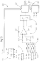
- FIG. 3 is the block diagram of an analog circuit according to the present invention.
- FIG. 3 essentially comprises four blocks which respectively symbolize a circuit for processing a signal 2, a first amplification / attenuation stage with variable gain 4, a block 6 grouping together gain control means and means for suppressing transients and, finally, a second amplification / attenuation stage with variable gain 8 to restore the signal to its original level.
- block 8 may be implicit. In the case of a multi-meter, for example, it is the operator who determines the measurement scale to be considered by knowing the position of the range selector.
- the general operating principle is as follows.
- the signal to be processed is firstly supplied by a line 10 at the input of the first amplification / attenuation stage 4 which, in response to this signal, outputs at a line 12 a signal whose amplitude is normalized .
- the amplification / attenuation stage 4 is provided to be controlled by the gain control means.
- the different values that the gain can take are denoted K0, K1, ..., K n .
- the gain can take either a set of discrete values (this is called a switchable gain), or vary continuously within a certain interval.
- the signal amplified by the amplification / attenuation stage is supplied, via line 12, to the input of the signal processing circuit 2.
- the circuit 2 In response to this signal on its input, the circuit 2 outputs a processed signal on a line 14.
- Signal processing can be of all known types (filtering, analysis, analog / digital conversion, etc.).
- a line 16 extending between a node 15 on the line 14 and the block 6.
- This line 16 is used to apply the level of the signal supplied at the output of the processing circuit 2 to the gain control means of block 6, so as to allow the latter to determine when the gain of stage 4 must be changed.
- Those skilled in the art will understand that instead of checking the level of the signal at the output of the processing circuit 2, it would also be possible to measure the level of the signal at the input, of the signal at the output of the first stage 4 or at any other place. of the diagram in Figure 3.
- the operating principle of the gain control means 6 is as follows; if at some point the signal level on line 16 exceeds a certain fraction, for example 90%, of the total dynamics of circuit 2 or if, on the contrary, this level falls below a certain fraction, for example 25 %, of the dynamics, the gain control means react by controlling the two amplification / attenuation stages 4 and 8 so as to change their gain, so as to reduce the level of the signal at the input of the processing circuit 2 to a value as close as possible to the maximum admissible by the latter.
- a certain fraction for example 90%
- the gain control means react by controlling the two amplification / attenuation stages 4 and 8 so as to change their gain, so as to reduce the level of the signal at the input of the processing circuit 2 to a value as close as possible to the maximum admissible by the latter.
- the two lines 18 and 20 are intended to supply each of the stages 4 and 8 a control signal in response to which each of stages 4 and 8 will change gain.
- the gain control means and the amplification / attenuation stages are provided to cooperate so that, when the gain of the first stage 4 changes in a given ratio, the gain of the second stage 8 changes in an inverse ratio to that from the first floor.
- Such an arrangement is important when for example the signal to be processed is an audio signal which one wishes to filter.
- the second amplification / attenuation stage 8 may not be explicitly present as in the measurement instruments already mentioned.
- the module 6 of FIG. 3 still comprises, according to the present invention, a sequencer which is associated with the gain control means, and which ensures, via line 22, the control of the suppression means transients according to the present invention.
- the means for suppressing transients are provided so as to modify the values of the state variables of the processing circuit 2 each time the gain of the amplification / attenuation stage 4 changes. Furthermore. the modification of the state variables is made in proportion to the variation of the gain of the first stage 4. Experience shows, in fact, that such a modification of the state variables makes it possible to almost completely remove the transients and the components undesirable in the output of the processing circuit 2.
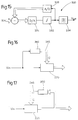
- the circuit shown diagrammatically in FIG. 4 constitutes a first particular example of a circuit for processing a signal which is generally represented in FIG. 3 by the block referenced 2.
- the diagram in FIG. 4 represents a continuous second order pass filter -band / low pass using operational amplifiers with transconductance and capacities (OTA-C). This type of filter is known to those skilled in the art. Indeed, it is widely used in analog integrated embodiments, for signal processing.
- OTA-C operational amplifiers with transconductance and capacities
- the circuit of FIG. 4 comprises an input line 12 for receiving a signal to be filtered supplied by the first amplification / attenuation stage (FIG. 3) and two output lines 14a and 14b intended to be used alternatively to provide either a low pass filtered signal or a band pass filtered signal.
- the circuit 2 comprises two capacitors, of capacitance C1 and C2 respectively, referenced 24a and 24b. These capacitors 24a and 24b are each connected between a node of the circuit (referenced 26a and 26b respectively) and the ground. As seen in the figure, the nodes 26a and 26b are each located downstream of an amplifier (referenced 28a and 28b respectively). It will be understood from the preamble to the description that, in the circuit shown here, it is the capacitors 26a and 26b which store the memory of the circuit. Consequently, in the present example, the state variables which must, in accordance with the present invention, be modified by the means for suppressing the transients are the respective charges of the two abovementioned capacitors.
- FIG. 5 represents one of the capacitors 24a or 24b of FIG. 4 with the means for suppressing the transients which, according to the present invention, are associated with it.
- the capacitor 24 of capacity C represents one of the capacitors 24a or 24b
- the node 26 represents one of the nodes 26a or 26b
- the transconductance amplifier 28 represents one of the transconductance amplifiers 28a or 28b.
- FIG. 5 The other elements shown in FIG. 5 are part of the means for suppressing transients according to the present invention.
- the particular means of suppressing the transients described in this first example are provided for a situation where the amplitude of the signal at the input of the circuit of FIG. 4 has previously been normalized by an amplification / attenuation stage, the gain of which can take different discrete values having between them relationships which are powers of 2.
- these means comprise a capacitor 30, having the same capacitance C as the capacitor 24, an operational amplifier 32 and seven switches referenced, respectively, ⁇ 1, ⁇ 1b, ⁇ 1c, S1, S2, S3 and S4.
- the circuit described in FIG. 5 is a circuit of the switched capacity type.
- the switches can be controlled by control signals conventionally generated by a sequencer (already mentioned in connection with FIG. 3) itself responding to the control signals produced by the gain control means (referenced 6 in FIG. 3 ).
- the control signals, generated by the sequencer are supplied to the various switches by transmission lines which are not shown.
- the means for suppressing the transients are therefore provided for modifying the values of the state variables by any power of 2.
- the sequencer controlling the transient suppression means, becomes operational. It first generates a first command signal to open the switches ⁇ 1 and ⁇ 1b and to close the switch ⁇ 1c and the switches S1 and S2. The first result of these switches is to isolate the first capacitor 24 and its contents from the rest of the circuit. In addition, closing the switch ⁇ 1c has the effect of connecting the capacitor 24 between the output and the virtual ground of the amplifier 32 so that its charge is, initially, kept constant. Finally, the closing of the switches S1 and S2 has the effect of completely discharging the second capacitor 30.
- the sequencer sends a second control signal to open the switches ⁇ 1c, S1 and S2 and close the switches S3 and S4 so as to connect the two capacitors 24 and 30 in parallel. Under these conditions, half of the charge present in the capacitor 24 passes through the capacitor 30 to equalize the voltages between the terminals of the two capacitors. This charge transfer has the effect of dividing by 2 the value of the state variable stored in the capacitor 24.
- the sequencer finally sends a third control signal to return the switches to their initial configuration (all switches open except ⁇ 1 and ⁇ 1b).
- the sequencer controlling the transient suppression means becomes operational. It first generates a first control signal identical to the first control signal of the divide by 2 sequence described above.
- This control signal has the effect open the switches ⁇ 1 and ⁇ 1b and close the switch ⁇ 1c.
- the first result of this switching is to isolate the capacitor 24 and its content from the rest of the circuit.
- closing the switch ⁇ 1c has the effect of connecting the capacitor 24 between the output and the virtual ground of the amplifier 32 so that its charge is, initially, kept constant.
- the sequencer sends a second control signal to close the switches S2 and S3.
- the operational amplifier 32 charges the capacitor 30 until the voltage between its terminals is equal to the voltage between the terminals of the capacitor 24.
- the capacity of the capacitor 30 being identical to that of the capacitor 24, it will contain the same charge as the latter.
- the sequencer then sends a third control signal to open the switches S2 and S3 and close the switches S1 and S4. Under these conditions, the charges contained in the capacitor 30 cause a modification of the potential at the inverting input of the amplifier 32 which, in response, provides charges to the capacitor 24 until the potential of its inverting input again that of mass. This last operation results in a doubling of the voltage between the terminals of the capacitor 24.
- the sequencer finally sends a fourth control signal to return the switches to their initial configuration (all the switches open except ⁇ 1 and ⁇ 1b).
- a switching sequence like that which has just been stated can be carried out in a much shorter time than the duration of the transient disturbances which are observed in the absence of the means for suppressing the transients according to the invention.
- the cut produced in the signal by the transient suppression means may even be imperceptible.
- the change of the state variables can be carried out within one or more periods of the carrier.
- FIG. 6 therefore represents a second embodiment of the means for suppressing transients according to the present invention.
- the means for suppressing the transients are used to change the value of the state variable associated with the capacitor 24b with capacitance C2 in FIG. 4.
- the components shown in FIG. 6 which are already shown in FIG. 4 have the same reference numbers.
- the circuit of FIG. 6 operates by virtue of a block 35 supplying a current at output, the intensity of which is equal to the product of the intensity of the input current by the amplitude of a control signal.
- This block 35 is adapted to, on the one hand, supply on its output 60 a current KI which is equal to K times the current I received on its input 50 and, on the other hand, to ensure that the input 50 remains at the mass.
- This block 35 can be produced in the manner presented to ISCAS 1989 by Adel S. Sedra under the title "the current conveyor; history and progress", and by using a current mirror with variable ratio.
- These means for removing transients comprise two identical capacitors, a first of the two (for example the capacitor 24) fulfilling at a given moment the function of the capacitor 24b in the circuit of FIG. 4.
- the first capacitor is discharged through block 35.
- Block 35 then supplies, at output, a current whose intensity is equal to the intensity of the current produced by the discharge of the first capacitor multiplied by a factor K given.
- the current at the output of block 35 is used to charge the second capacitor which, at the end of the operation, has between its terminals a voltage equal to the voltage which previously existed between the terminals of the first capacitor multiplied by said given factor.
- the circuit of FIG. 6 includes a switch 1 which corresponds to the switch 1 of FIG. 5 and a series of pairs of switches S1a, S1b, S2a, s2b, S3a, S3b, S4a, S4b, S6a, S6b, S7a and S7b.
- the capacitor 24 is associated with the switches Sa while the capacitor 24 'is associated with the switches Sb.
- a resistor 37 is finally mounted at the input of the multiplier 35 to slow the discharge of the capacitor when the value of the state variable changes.
- the switch 1 In the absence of a gain change in the amplification / attenuation stage, the switch 1 is closed. We will assume here that before the gain change, the capacitor 24 was connected to the filter. Under these conditions, the switch S1a is closed and the switch S1b is open. In addition, the switches S3a, S4a, S6a and S7a are also open while the switch S2a is closed. Note also that the switches S2b and S7b are closed to keep the capacitor 24 'fully discharged and that the switches S3b, S4b and S6b are open.
- the sequencer controlling the transient suppression means becomes operational. It generates, on the one hand, a first control signal to open the switch 1 and decouple the capacitor 24 from the rest of the circuit and on the other hand it transmits to block 35 a signal corresponding to the given factor by which the gain at input of the filter will be multiplied.
- the switches S4a, S7a, S2b and S6b are closed while the switch S2a is open.
- the capacitor 24 will discharge through the resistor 37 in the input of the block 35.
- all the current supplied at the output of the multiplier 35 will accumulate in the capacitor 24 '.
- the charge which will accumulate in the capacitor 24 ′ will be proportional to the charge initially contained by capacitor 24.
- the multiplication factor K of block 35 being determined by the factor by which the gain control means modifies the gain, the ratio between the charge of the capacitor 24 'and that of the capacitor 24 will be equal to the factor by which the gain is changed.
- the sequencer sends a control signal to close the switch S1b and close the switch 1 so as to couple the capacitor 24 'with the circuit.
- FIG. 7 shows another example of application of the present invention.
- the device shown diagrammatically in FIG. 7 is designed to provide a variable signal at the output in response to a variable quantity picked up at the input by a sensor which in the present example is of the capacitive type.
- the device firstly comprises a capacitive sensor with two capacitors 110.
- the output of the sensor 110 is connected to the input of a processing and interface circuit 120 which can typically be constituted by a Sigma-Delta bandpass modulator.
- the Sigma-Delta 120 modulator provides a bit train modulated in pulse density.
- This bit stream is supplied to a synchronous digital detection module 130 controlled by a time base signal supplied on a line 180 by a clock. 160.
- the module 130 supplies in response a digital signal which constitutes the output signal of the device.
- the bit stream produced by the processing circuit 120 is also supplied to a module 140 which essentially functions as a low-pass filter to produce an analog output signal from the pulse density modulated signal.
- the analog signal produced by the module 140 is still transmitted by a line 170 to the sensor 110 so as to constitute a feedback loop to, for example, maintain the sensor in a state of equilibrium .
- the capacitive sensor 110 may, in known manner, be of the type comprising two capacitors and in which a movable conductive strip constitutes a common movable frame for the two capacitors. With such an arrangement, any movement of the movable blade results in a variation of the respective capacities of the two capacitors. This variation in the capacitances of the two capacitors is typically measured by respectively placing the fixed plates of the two capacitors with two imposed potentials of the same value but with opposite signs, and by measuring either the charge or the potential on the moving blade. It should be noted that with such an arrangement the intensity of the measurement signal, or in other words the sensitivity of the sensor, is proportional to the modulus of the potential imposed on the fixed armatures.
- the devices corresponding to the part of the functional diagram of Figure 7 which has been described so far can be made with known elements.
- a particular example of such a device is the device for measuring a force described in document EP 0 590 658.
- a modulator such as that described in the article entitled "A Fourth -Order Bandpass Sigma-Delta Modulator "by Stephen A. Jantzi et al. and appeared in the IEEE Journal of Solid-State Circuits, Vol. 28, No. 3, March 1993.
- the device of FIG. 7 also comprises a module 150 which fulfills the same functions as the means represented by block 6 in FIG. 3.
- the module or block 150 controls the level at the output of the treatment circuit 120 at l using line 154 so as to determine when the sensitivity of sensor 110 should be changed.
- FIG. 7 also shows a control line 156 which allows the block 150 to control a block 100 which is provided to supply the two reference potentials for the fixed armatures of the capacitive sensor 110.
- the processing circuit 120 includes a memory
- the variations caused by the sensitivity of the sensor will, as in the case of the device in FIG. 3, cause the appearance of transients.
- the device of FIG. 7 comprises means for suppressing the transients (symbolized by the line 190) which can be produced in a completely analogous manner to those which have been described with reference to FIG. 5 or to Figure 6.
- FIG. 8 it can be seen that it represents a sigma-delta converter 220 at multiple ranges comprising a signal combination circuit 221, an integrator 222, a comparator 223, a feedback circuit 224, an amplifier 225 of the input signal, a range adjustment circuit 226, an amplifier 227 of the signal output Y and a noise compensation circuit 228.
- the input signal amplifier 225 comprises four capacitors 229, 230, 231 and 232. One of the plates of capacitors 229, 230, 231 and 232 is connected respectively to one of the terminals of the switches 233, 234, 235 and 236.
- the integrator 222 comprises an operational amplifier 237, a capacitor 238 of which is connected between its inverting input and its output.
- the integrator 222 generates, at its output, an analog voltage which represents the integration with respect to time of the total charge stored by the capacitors 229 to 232 and 257.
- the other terminals of the switches 233, 234, 235 and 236 are connected set at the inverting input of the operational amplifier 237 via a switch 239.
- Two terminals 240 and 241 are connected to the input signal amplifier 225 via two switches 242 and 243 of so that an analog voltage V in present at these terminals can be applied to one or more of the capacitors 229, 230, 231 and 232.
- the capacitors 229, 230, 231 and 232 have the same value C in .
- the range setting circuit 226 includes a switch control circuit 244 and the switches 233, 234, 235 and 236.
- a data bus 245 transmits a signal which represents the desired gain G of the input signal of the sigma converter. delta 220, to circuit 244 for controlling switches.
- This circuit has four outputs 244a, 244b, 244c and 244d to respectively control the operation of switches 233, 234, 235 and 236.
- the operation of switches 233, 234, 235 and 236 is controlled respectively as a function of the gain signal received from the bus 245, so that the input voltage V in present between the terminals 240 and 241 can be applied to one of the capacitors 229, 230, 231 and 232 or to a combination of these capacitors connected in parallel.
- the noise compensation circuit 228 comprises a circuit 250 for controlling switches and gain detection intended to detect a variation in the value of the gain signal coming from the bus 245 and to control the respective operation of the contactors 246, 247, 248 and 249 via its outputs 250a, 250b, 250c and 250d, so that the capacitors 238 and 245 are connected, either in parallel or in series between the operational amplifier 237 and the ground.
- the comparator 223 compares the voltage level at the output of the operational amplifier 237 with a predetermined reference voltage, which is in the case shown, the ground potential. If the output voltage of the operational amplifier is greater than zero volts, the comparator produces a bit of value +1 at its output, while when this voltage is less than zero volts it produces a bit of value -1. In the data bit stream, carrying the reference Y, which is thus produced by the comparator 223, the density of the bits of high logic level relative to that of the level bits logic low, represents the analog input voltage V in applied between terminals 240 and 241.
- the feedback circuit 224 comprises a bit detector and a circuit 251 for controlling switches, two terminals 252 and 253, switches 239, 254, 255 and 256, a capacitor 257 having a value C ref and a source of voltage V ref (not shown).
- the control circuit 251 has outputs 251a and 251b to allow the control of the switches 254 and 255, respectively.
- the switches 254 and 255 allow the capacitor 257 to be changed with a charge Qref equal to C ref * V ref , or to discharge this capacitor.
- the load Q ref is integrated in the positive direction or in the negative direction. The difference between the charges Q in ⁇ Q ref is thus stored between the armatures of the capacitor 238 and correspondingly integrated by the operational amplifier 237.
- the stability of the sigma-delta converter 220 is guaranteed as long as the charge Q in associated with the input signal is less than the absolute value of the charge Q ref injected by feedback.
- the input signal V in can thus be sampled with a gain of 1, 2, 3 or 4 in controlling switches 233, 234, 235 and 236 so as to choose the corresponding number of capacitors 229, 230, 231 or 232.
- the multiplication of the input signal by a desired gain can be achieved in another way, for example by a programmable current mirror or by other circuits in which the active elements are different from capacitors 229, 230, 231 and 232.
- the gain chosen can be greater or less than 1 and take values other than positive integers (1, 2, 3 and 4) of FIG. 8.
- positive integers as gain values simplifies the operation of the division performed by logic circuit 227.
- the values of the chosen gain correspond to powers of two (that is to say the gain can take values such as 4, 2, 1, 1 / 2, 1 / 4, ...) so that the division of the digital word produced by the logic circuit 227 implies a simple shift of the bits in the word.
- the voltage V amp should be equal to ⁇ t1 2 (Vin * Cin - X * Vref * Cref).
- the charge stored by the capacitor 238 remains at this instant always equal to ⁇ t1 (V in * C in - X * V ref * C ref ), so that there is no longer a correct relationship between the function of the integrator and the charge on its capacitor.
- the circuit 250 for controlling the switches momentarily closes the switches 247 and 248 which charges the capacitor 245 has the same value as the capacitor 238. Then the switches 247 and 248 are open, then the switches 246 and 249 are closed. Thus, the capacitor 245 is discharged and its charge is transferred to the armatures of the capacitor 238.
- the switch control circuit 250 first discharges the capacitor 245 by temporarily closing the switches 248 and 249. Then the switches 246 and 247 are closed, which connects the capacitor 245 in parallel with the capacitor 238. If a value equal to that of the capacitor 238 is chosen for the capacitor 245, the charge stored between the plates of the capacitor 238 is reduced by half. The capacitor 245 is then disconnected from the integrator 222. The charge stored by the integrator 222 then becomes ⁇ t1 (V in * C in - X * V ref * C ref ) and the error which is accumulated there is reduced by half to compensate for the halving of the chosen gain.
- the sigma-delta converter in Figure 8 is a particular example of how the switching noise that results from a change in the range of the input signal can be compensated for by multiplying the error accumulated in l 'integrator by a ratio R of the newly chosen gain compared to the previously chosen gain.
- This operation can be implemented more easily if the relation R between the various successive gains is constant, because in this case, it suffices to carry out a multiplication and a division of the error accumulated by the relation R.
- the value of R can conveniently be equal to 2.
- the use of capacitors 238 and 245 in Figure 8 is a practical example of such an embodiment.
- the sigma-delta converter described with reference to FIG. 8 converts an analog input voltage into a digital output word, but it is clear that, according to the present invention, the use of this converter is not limited to this application.
- the invention can be applied in the case where a capacitance is measured which is converted into a variable output signal.
- the capacitors 229, 230, 231 and 232 can be replaced by a voltage source having four predetermined values which are applied across the capacitors to be measured according to a chosen gain of the input signal.
- the input signal applied to the sigma-delta converter of the present invention may be an analog current directly sent to the integrator 222, in which case the input signal amplifier comprises an adjustable current amplifier or a network of resistors.
- the input signal amplifier comprises an adjustable current amplifier or a network of resistors.
- FIG. 9 shows an oversampling digital / analog converter 270 comprising a multi-range sigma-delta converter 271 intended to convert a digital quantity at n bits into a digital quantity at m bits.
- the converter 270 includes a digital interpolation filter 272, an elementary digital / analog converter 273 and an analog low-pass filter 274.
- An input signal X is constituted by an n-bit digital word which is applied to the interpolation filter 272.
- the signal X is first interpolated and then sampled at a frequency f s in the filter interpolation 272, f s being significantly greater than the Nyquist frequency f N of the input signal X.
- the sigma-delta converter 271 is used as a digital noise conformator, operating at a frequency d 'clock f s , which "approximates" the signal X1 of the interpolation filter so as to obtain a signal X2 which consists of a digital word with m bits, n> m.
- the noise generated by the approximation is thus rejected towards frequencies higher than the sampling frequency f s .
- the word "approximate" X2 is converted into an analog signal V1 by the elementary digital / analog converter 273 before passing through the low-pass filter 274 which eliminates the approximation noise rejected towards the higher frequencies.
- the oversampling digital / analog converter 270 also includes a bus 275 intended to apply the chosen gain G to the sigma-delta converter 271 and to the elementary D / A converter 273.
- the signal X1 is multiplied by the gain G so that the signal X2 is better suited to the input range of the elementary D / A converter 273.
- the signal X2 has been converted to analog form, it is divided by G so that the filtered output signal V out represents the digital input signal X.
- a sigma-delta converter (digital noise shaper) 280 has been represented comprising an integrator 281, a truncator 282 and a subtraction circuit 283.
- the integrator 281 comprises a digital register 284 and an addition circuit 285.
- a digital signal X in with n bits is applied to the converter 280.
- a digital signal Y out with m bits which will be described briefly below, n> m, is subtracted from the signal X in and the resulting signal X diff at n bits is applied to the integrator 281.
- the integration is carried out according to an algorithm which adds the output of the register 284 generated during a cycle of previous clock at signal X diff and temporarily stores the resulting sum in the register during the current clock cycle.
- the n bit signal X in from the integrator 281 is truncated to form an output signal Y out comprising the m most significant bits of the signal X int .
- the signal Y out also provides a feedback signal which is subtracted from the input signal X in by the subtraction circuit 283.
- a comparison of the sigma-delta converter of FIG. 1 with the digital noise shaper of FIG. 10 shows that the analog input signal is replaced by a n-bit digital signal, that the integrator 202 is replaced by the integrator 281 purely digital and the comparator 203 is replaced by the truncator 282.
- the output of the D / A converter 204 is replaced by the signal Y out which does not need a physical circuit to be generated due to the division of the bus X int in two parts by the truncator 282.
- the circuit 206 for combining signals is replaced by the subtraction circuit 283.
- the digital noise shaper 280 of Figure 10 is a functional equivalent of the sigma-delta converter 201 of Figure 1.
- the digital noise shaper 280 interpolates and oversamples the signal X in at n bits of so as to produce an output signal Y out which provides an estimate at m bits of the input signal X in .
- the quantization error resulting from the sampling process is rejected towards the higher frequencies by the integrator which is used to carry out the sigma-delta conversion.
- FIG. 10 shows a digital noise shaper 290 in which this simplification has been implemented.
- the digital noise shaper 290 includes the digital register 284, the truncator 282 and the addition circuit 285 of FIG. 10, however that in this embodiment of the invention, the most significant bits Y lsb are accumulated up to that they produce an overshoot of the Y msb signal and are thus transferred to the output of the Y out clipper.
- the converter 290 thus stores the conversion error between its input signal and its output signal.
- a variation in the gain of the input signal alters the relationship between the function of the integrator and the digital value stored in the accumulator, which can be avoided by multiplying the conversion error by the ratio of new gain to old gain.
- FIG. 12 shows an embodiment of the sigma-delta converter 271 with multiple ranges of FIG. 9.
- the latter comprises the converter 290 of FIG. 11 and two multiplication circuits 291 and 292.
- the multiplication circuit 291 multiplies the signal d input X in by the gain signal G (k) chosen from the bus 275.
- the value of the gain G (k) can be changed according to the choice of the range of the input signal from the converter 271.
- the error between the input signal X in and the output signal Y out is accumulated in the digital accumulator 284 with a gain which depends on the chosen range, the change in the range of the input signal introduces switching noise into the stored conversion error.
- the multiplication circuit 292 is connected in the feedback circuit between the truncator 282 and the addition circuit 285, in order to multiply the signal Y lsb by the ratio of the new gain G (k) to the old gain G (k-1).
- the position of the bits in each of the digital words X in and Y lsb can be offset by an appropriate number of locations. This can preferably be done using shift registers, the gain signals G (k) and G (k) / G (k-1) determining the number of positions by which the bits are to be shifted.
- FIG. 13 shows in general a sigma-delta A / D converter 100 comprising the integrator 222, the comparator 223 and an amplifier 227 of the output signal of the sigma-delta converter 220.
- the sigma-delta converter 300 comprises a signal combining circuit 301, an amplifier 302 of the signal of feedback, a range setting circuit 303 and a feedback circuit 304.
- the feedback amplifier 302 comprises four capacitors 305, 306, 307 and 308.
- the armatures of these capacitors are respectively connected to the switch terminals 309, 310, 311 and 312.
- the other terminals of these switches are connected together to the non-inverting input of an operational amplifier 237 via switch 256.
- the voltage V ref present at terminals 252 and 253 is applied to one or more of the capacitors 305, 306, 307 and 308.
- these capacitors Preferably, these capacitors have the same value C ref .
- the range adjustment circuit 303 comprises a circuit for controlling switches 313 as well as switches 309, 310, 311 and 312.
- the circuit 313 has four outputs 313a, 313b, 313c and 313d for controlling the operation of the switches 309 respectively. 310, 311 and 312.
- the operation of the switches is selectively controlled as a function of the gain signal from the bus 245 so that any combination of the capacitors 305, 306, 307 and 308 can be connected so as to receive the voltage V ref .
- the charge stored between the armatures of the capacitors connected in parallel can thus be equal to C ref * V ref , 2C ref * V ref , 3C ref * V ref or 4C ref * V ref , depending on the gain that is present on the bus. 245.
- the input signal V in present between terminals 240 and 241 is applied to the terminals of a capacitor 314 whose value is C in , by means of switches 242 and 243.
- a charge Q in equal to V in * C in is thus produced between the armatures of the capacitor C in .
- This load is applied to the inverting input of the operational amplifier 237 via the switch 239.
- the feedback circuit 304 includes a control circuit 315, terminals 252 and 253, the contactors 239, 254, 255 and 256 and the voltage source V ref .
- the control circuit 315 detects the digital word at the output of the amplifier 227 of the output signal, this word resulting from the multiplication of the digital information in the bit stream coming from the comparator 223 by the inverse of the gain on the bus 245.
- the control circuit 315 has outputs 315a and 315b to allow control of the operation of the switches 254 and 255, respectively.
- the load G * Q ref is integrated either positively or negatively depending on the value +1 or -1 of the bit produced at the output of comparator 223, by controlling the operation of switches 254 and 255.
- the difference between the charges Q in ⁇ G * Q ref is stored between the armatures of the capacitor 238 and is thus integrated by the operational amplifier 237.
- the sigma-delta converter 300 is stable as long as the charge Q in is less than the absolute value of the reaction charge Q ref .
- the range of the input signal for the input signal V in can thus be chosen according to the number N of capacitors 305, 306, 307 and 308 connected in parallel.
- the capacitor 238 of the integrator 222 accumulates the difference between the analog input signal and the digital output signal reconverted into analog form.
- the switching noise is introduced at the moment when the range of the input signal is modified due to the alteration of the relation between the gain of the input signal V in and the quantization error stored by the capacitor 238. This noise is avoided by multiplying the quantization error by the ratio of the new gain to the old gain.
- the integrator 222 accumulates the quantization error independently of the gain chosen.
- the output V amp of the operational amplifier 222 is equal to A ( ⁇ t1 e (t) .dt), where A represents the fixed gain of the input signal V in . Any alteration of the relationship between the gain of the input signal and the error accumulated in the integrator of the sigma-delta converter and consequently any switching noise which could result therefrom is thus avoided.
- the sigma-delta converter 300 of FIG. 13 can also be produced in the form of a digital noise shaper intended to convert a digital signal of n bits into a digital signal of m bits.
- FIG. 14 shows, in general, such a sigma-delta converter 320 comprising the digital accumulator 284 and the addition circuit 285 of FIG. 12 and, moreover, a programmable truncator 321.
- the number of bits in the signal Y lsb and consequently of the complementary signal Y msb is modified by the truncator 321 in response to the value of the selected gain G which is applied to it; which allows the converter 321 reaction circuit to be programmed.
- the sensitivity of the converter 321 can be increased by reducing the number of the least significant bits accumulated and consequently by producing a faster exceeding these bits in the most significant bit of signal X1.
- the accumulator always accumulates the difference between the input signal X in and the output signal Y out regardless of the range chosen for the converter 320, the digital value stored in the accumulator 284 need not be update, when the chosen range is modified.
- the sigma-delta converter in FIG. 14 has the advantage of greater simplicity compared to the sigma-delta converter 271 represented in FIG. 12.
- FIG. 15 represents, in general, a digital / analog converter 330 with oversampling mounted in closed loop.
- the converter 330 has a direct circuit with a basic D / A converter 331 and an integrator 332, as well as a feedback circuit which includes an analog / digital converter 333.
- a low-low filter 334 eliminates high frequency noise of the voltage at the output of the integrator 332.
- the accuracy of the sigma-delta converter 330 is essentially determined by the feedback circuit.
- the sigma-delta converter 330 can thus be produced by using a precise A / D converter 333 and a more basic D / A converter 331.
- the sigma-delta converter of the The present invention in the form described for example in connection with FIGS. 8 and 13, is thus ideally suited for use as an A / D converter 333. It is preferable, to confer on the sigma-delta converter of the present invention the best signal-to-noise ratio, optimizing the chosen gain. If the gain chosen is too high, the converter will saturate when either the input signal or the feedback signal exceeds a certain amplitude. This results in "truncation" of the signal and distortion of the output signal. On the other hand, if the gain chosen is too low, the operation of the converter leads to a low resolution and the signal-to-noise ratio is reduced.
- FIG. 16 schematically represents the sigma-delta converter 220 of FIG. 8 and a gain control circuit 340, the latter being able to be used also in the other embodiments of the invention.
- This circuit 340 measures the amplitude of the signal V in but can also measure its energy. Depending of this measured amplitude, the control circuit 340 increases or decreases the value of the gain G on the bus 245 so that it can be used by the sigma-delta converter 220 for adjusting the range of the input signal.
- the control circuit 340 will not be described in detail, because it can be easily carried out by specialists; it can for example comprise a mixed analog / digital circuit comprising threshold detectors, comparators, Schmitt "triggers", low pass filters and / or low resolution A / D converters by means of which this circuit checks the level of the input signal and consequently adjusts the sensitivity of the converter 220 by sending a signal representing the range chosen to the range selection circuit of the converter 220.
- FIG. 17 shows another arrangement in which the sigma-delta converter 220 of FIG. 8 is controlled by a gain control circuit 350 which measures the level of the signal at the output of the converter 220. As the circuit used is then practically only digital, the gain control circuit 220 thus avoids the use of additional analog circuits of the gain control circuit 340 of FIG. 16.
- the scope of the present invention is not limited to circuits comprising a variable gain input stage but that it generally extends to all devices in which the amplitude of a magnitude captured at input can vary predictably and whose variation has an effect comparable to a change in gain.
- the invention remains applicable when the amplitude of the signal undergoes changes, predictable or detectable, comparable to a change in gain due to a disturbance, a change in the characteristics of the processing circuits, etc.
Landscapes
- Engineering & Computer Science (AREA)
- Theoretical Computer Science (AREA)
- Compression, Expansion, Code Conversion, And Decoders (AREA)
- Control Of Amplification And Gain Control (AREA)
- Measuring Instrument Details And Bridges, And Automatic Balancing Devices (AREA)
- Measurement Of Current Or Voltage (AREA)
- Filters That Use Time-Delay Elements (AREA)
- Tone Control, Compression And Expansion, Limiting Amplitude (AREA)
- Picture Signal Circuits (AREA)
Applications Claiming Priority (4)
| Application Number | Priority Date | Filing Date | Title |
|---|---|---|---|
| FR9307950A FR2708161B1 (fr) | 1993-06-28 | 1993-06-28 | Convertisseur sigma-delta à plusieurs plages. |
| FR9307950 | 1993-06-28 | ||
| FR9403541A FR2717933B1 (fr) | 1994-03-25 | 1994-03-25 | Circuit de traitement de signaux comportant un étage d'entrée à gain variable. |
| FR9403541 | 1994-03-25 |
Publications (2)
| Publication Number | Publication Date |
|---|---|
| EP0631395A1 true EP0631395A1 (de) | 1994-12-28 |
| EP0631395B1 EP0631395B1 (de) | 1999-03-24 |
Family
ID=26230447
Family Applications (1)
| Application Number | Title | Priority Date | Filing Date |
|---|---|---|---|
| EP94109610A Expired - Lifetime EP0631395B1 (de) | 1993-06-28 | 1994-06-22 | Schaltung zur Verarbeitung von Signalen mit einer Eingangsstufe mit veränderbarer Verstärkung |
Country Status (6)
| Country | Link |
|---|---|
| US (1) | US5541600A (de) |
| EP (1) | EP0631395B1 (de) |
| JP (1) | JP3530587B2 (de) |
| AT (1) | ATE178171T1 (de) |
| CA (1) | CA2126525C (de) |
| DE (1) | DE69417296T2 (de) |
Cited By (2)
| Publication number | Priority date | Publication date | Assignee | Title |
|---|---|---|---|---|
| EP0660527A1 (de) * | 1993-12-16 | 1995-06-28 | AT&T Corp. | Datenwandler mit Skalierung der Verstärkung zusammen mit einem Zittersignal |
| EP0809842A4 (de) * | 1995-01-30 | 1999-01-20 | Noise Cancellation Tech | Adaptiver sprechfilter |
Families Citing this family (52)
| Publication number | Priority date | Publication date | Assignee | Title |
|---|---|---|---|---|
| US5731767A (en) * | 1994-02-04 | 1998-03-24 | Sony Corporation | Information encoding method and apparatus, information decoding method and apparatus, information recording medium, and information transmission method |
| JPH08223049A (ja) * | 1995-02-14 | 1996-08-30 | Sony Corp | 信号符号化方法及び装置、信号復号化方法及び装置、情報記録媒体並びに情報伝送方法 |
| JP3307138B2 (ja) * | 1995-02-27 | 2002-07-24 | ソニー株式会社 | 信号符号化方法及び装置、並びに信号復号化方法及び装置 |
| US5960390A (en) * | 1995-10-05 | 1999-09-28 | Sony Corporation | Coding method for using multi channel audio signals |
| US5731769A (en) * | 1995-12-04 | 1998-03-24 | Motorola, Inc. | Multi-rate digital filter apparatus and method for sigma-delta conversion processes |
| US5825320A (en) * | 1996-03-19 | 1998-10-20 | Sony Corporation | Gain control method for audio encoding device |
| US5821889A (en) * | 1996-11-06 | 1998-10-13 | Sabine, Inc. | Automatic clip level adjustment for digital processing |
| US5859605A (en) * | 1997-01-24 | 1999-01-12 | Hughes Electronics Corporation | Digital waveform generator and method for synthesizing periodic analog waveforms using table readout of simulated Δ- Σ analog-to-digital conversion data |
| US5905398A (en) * | 1997-04-08 | 1999-05-18 | Burr-Brown Corporation | Capacitor array having user-adjustable, manufacturer-trimmable capacitance and method |
| US5916179A (en) * | 1997-04-18 | 1999-06-29 | Sharrock; Nigel | System and method for reducing iatrogenic damage to nerves |
| US6097251A (en) * | 1998-05-29 | 2000-08-01 | Telefonaktiebolaget Lm Ericsson | Pre-recorded sigma delta values for power amplifier control |
| US6005500A (en) * | 1997-06-06 | 1999-12-21 | Rosemount, Inc. | Transmitter with improved analog to digital converter |
| US5892472A (en) * | 1997-06-30 | 1999-04-06 | Harris Corporation | Processor controlled analog-to-digital converter circuit |
| JP3449254B2 (ja) * | 1997-11-14 | 2003-09-22 | ヤマハ株式会社 | D/a変換装置 |
| US6160859A (en) * | 1998-10-19 | 2000-12-12 | Motorola, Inc. | Integrated multi-mode bandpass sigma-delta receiver subsystem with interference mitigation and method of using the same |
| US6204787B1 (en) | 1999-03-31 | 2001-03-20 | Cirrus Logic, Inc. | Circuits and methods for gain ranging in an analog modulator and systems using the same |
| DE10021824C2 (de) * | 1999-05-07 | 2002-01-31 | Yamaha Corp | D/A-Wandlervorrichtung und D/A-Wandlerverfahren |
| IT1313390B1 (it) * | 1999-07-16 | 2002-07-23 | St Microelectronics Srl | Metodo di ottimizzazione dei parametri di un filtro passabasso di pre-equalizzazione per canale di lettura. |
| FR2797725B1 (fr) * | 1999-08-16 | 2001-11-09 | St Microelectronics Sa | Procede et dispositif de conversion d'un signal analogique en un signal numerique avec controle automatique de gain |
| US6310567B1 (en) * | 1999-09-07 | 2001-10-30 | Linear Technology Corporation | Programmable configuration, level and output voltage range circuits and methods for signal processors |
| US6492924B2 (en) | 1999-09-07 | 2002-12-10 | Linear Technology Corporation | Circuits, systems, and methods for signal processors that buffer a signal dependent current |
| US6369740B1 (en) | 1999-10-22 | 2002-04-09 | Eric J. Swanson | Programmable gain preamplifier coupled to an analog to digital converter |
| US6590517B1 (en) | 1999-10-22 | 2003-07-08 | Eric J. Swanson | Analog to digital conversion circuitry including backup conversion circuitry |
| US6310518B1 (en) | 1999-10-22 | 2001-10-30 | Eric J. Swanson | Programmable gain preamplifier |
| US6414619B1 (en) | 1999-10-22 | 2002-07-02 | Eric J. Swanson | Autoranging analog to digital conversion circuitry |
| US6657570B1 (en) * | 2000-06-22 | 2003-12-02 | Adc Telecommunications, Inc. | Automatic level control for input to analog to digital converter |
| AU2001284726A1 (en) * | 2000-10-02 | 2004-03-03 | The Trustees Of Columbia University In The City Of New York | Circuit and method for dynamically modifiable signal processor |
| CN1582534B (zh) * | 2001-02-08 | 2010-05-12 | 模拟设备股份有限公司 | 可变全刻度的多比特σ-δ模数变换器 |
| US6452521B1 (en) * | 2001-03-14 | 2002-09-17 | Rosemount Inc. | Mapping a delta-sigma converter range to a sensor range |
| DE10118157A1 (de) * | 2001-04-11 | 2002-10-24 | Infineon Technologies Ag | Rückgekoppelter A/D- bzw. D/A-Wandler mit reduziertem Stromverbrauch |
| DE10219216B4 (de) * | 2002-04-29 | 2005-04-07 | Eads Astrium Gmbh | Verfahren und Endgerät zur Verarbeitung eines Navigationssignals in einem Satelliten-Navigationssystem |
| KR100610478B1 (ko) * | 2004-05-06 | 2006-08-08 | 매그나칩 반도체 유한회사 | 이미지센서 및 그의 디지털 이득 보상 방법 |
| KR100615535B1 (ko) * | 2004-07-26 | 2006-08-25 | 삼성전자주식회사 | Agc를 이용한 무선 수신장치 및 수신방법 |
| US7268715B2 (en) * | 2004-10-29 | 2007-09-11 | Freescale Semiconductor, Inc. | Gain control in a signal path with sigma-delta analog-to-digital conversion |
| US7126513B1 (en) * | 2005-09-27 | 2006-10-24 | Micrel, Incorporated | Analog control of a digital decision process |
| US7245148B2 (en) * | 2005-09-27 | 2007-07-17 | Micrel, Inc. | Power saving method in an integrated circuit programming and control circuit |
| US9425747B2 (en) * | 2008-03-03 | 2016-08-23 | Qualcomm Incorporated | System and method of reducing power consumption for audio playback |
| US8487639B1 (en) | 2008-11-21 | 2013-07-16 | Cypress Semiconductor Corporation | Receive demodulator for capacitive sensing |
| US8866500B2 (en) * | 2009-03-26 | 2014-10-21 | Cypress Semiconductor Corporation | Multi-functional capacitance sensing circuit with a current conveyor |
| US8717211B2 (en) | 2010-11-30 | 2014-05-06 | Qualcomm Incorporated | Adaptive gain adjustment system |
| US9268441B2 (en) | 2011-04-05 | 2016-02-23 | Parade Technologies, Ltd. | Active integrator for a capacitive sense array |
| US9778074B2 (en) * | 2013-03-14 | 2017-10-03 | Rosemount Inc. | Process measurement system with variable amplitude sensor excitation |
| CN103684458B (zh) * | 2013-12-16 | 2017-04-05 | 华为技术有限公司 | 模数转换器保护电路、数字电源、数字信号的处理方法和处理模块及电路保护方法 |
| US9548722B2 (en) | 2014-10-22 | 2017-01-17 | Analog Devices Global | Apparatus and methods for reducing glitches in digital step attenuators |
| GB2532015B (en) * | 2014-11-04 | 2018-12-26 | Cirrus Logic Int Semiconductor Ltd | Improved analogue-to-digital convertor |
| US10778206B2 (en) | 2018-03-20 | 2020-09-15 | Analog Devices Global Unlimited Company | Biasing of radio frequency switches for fast switching |
| WO2020084401A1 (en) | 2018-10-26 | 2020-04-30 | Sendyne Corporation | Improved runtime-calibratable analog computing system and methods of use |
| JP7525484B2 (ja) * | 2019-05-29 | 2024-07-30 | ソニーセミコンダクタソリューションズ株式会社 | アナログ-デジタル変換装置、アナログ-デジタル変換装置の制御方法、及び、オーディオ装置 |
| US11152917B1 (en) | 2020-05-28 | 2021-10-19 | Analog Devices International Unlimited Company | Multi-level buffers for biasing of radio frequency switches |
| WO2022202772A1 (ja) * | 2021-03-24 | 2022-09-29 | ヌヴォトンテクノロジージャパン株式会社 | アナログデジタル変換回路 |
| US11863227B2 (en) | 2021-10-25 | 2024-01-02 | Analog Devices International Unlimited Company | Radio frequency switches with fast switching speed |
| EP4618413A1 (de) * | 2024-03-15 | 2025-09-17 | Nxp B.V. | Anordnung mit variabler verstärkung |
Citations (8)
| Publication number | Priority date | Publication date | Assignee | Title |
|---|---|---|---|---|
| US3921012A (en) * | 1974-11-11 | 1975-11-18 | Mdh Ind Inc | Wide-range current-to-frequency converter |
| FR2300993A1 (fr) * | 1975-02-12 | 1976-09-10 | Messerschmitt Boelkow Blohm | Procede et dispositif d'adaptation de plage |
| US4851841A (en) * | 1987-10-02 | 1989-07-25 | Crystal Semiconductor Corporation | Gain scaling of oversampled analog-to-digital converters |
| EP0338837A2 (de) * | 1988-04-20 | 1989-10-25 | Nec Corporation | Analog-Digitalwandlerschaltung mit hoher Auflösung und niedriger Leistungsaufnahme |
| JPH02170723A (ja) * | 1988-12-23 | 1990-07-02 | Yamaha Corp | A/d変換回路 |
| EP0378777A2 (de) * | 1989-01-19 | 1990-07-25 | Daimler-Benz Aerospace Aktiengesellschaft | Anordnung zur Umsetzung analoger Signale in digitale |
| US5134401A (en) * | 1991-03-12 | 1992-07-28 | Analog Device, Inc. | Delta sigma modulator having programmable gain/attenuation |
| US5187482A (en) * | 1992-03-02 | 1993-02-16 | General Electric Company | Delta sigma analog-to-digital converter with increased dynamic range |
Family Cites Families (2)
| Publication number | Priority date | Publication date | Assignee | Title |
|---|---|---|---|---|
| US4185246A (en) * | 1978-02-27 | 1980-01-22 | Schlumberger Technology Corporation | Circuit for reducing transients by precharging capacitors |
| JP2615519B2 (ja) * | 1990-11-30 | 1997-05-28 | 松下電器産業株式会社 | 超音波ドプラ血流計 |
-
1994
- 1994-06-22 AT AT94109610T patent/ATE178171T1/de not_active IP Right Cessation
- 1994-06-22 CA CA002126525A patent/CA2126525C/en not_active Expired - Fee Related
- 1994-06-22 EP EP94109610A patent/EP0631395B1/de not_active Expired - Lifetime
- 1994-06-22 DE DE69417296T patent/DE69417296T2/de not_active Expired - Fee Related
- 1994-06-23 US US08/264,645 patent/US5541600A/en not_active Expired - Lifetime
- 1994-06-28 JP JP16751194A patent/JP3530587B2/ja not_active Expired - Fee Related
Patent Citations (8)
| Publication number | Priority date | Publication date | Assignee | Title |
|---|---|---|---|---|
| US3921012A (en) * | 1974-11-11 | 1975-11-18 | Mdh Ind Inc | Wide-range current-to-frequency converter |
| FR2300993A1 (fr) * | 1975-02-12 | 1976-09-10 | Messerschmitt Boelkow Blohm | Procede et dispositif d'adaptation de plage |
| US4851841A (en) * | 1987-10-02 | 1989-07-25 | Crystal Semiconductor Corporation | Gain scaling of oversampled analog-to-digital converters |
| EP0338837A2 (de) * | 1988-04-20 | 1989-10-25 | Nec Corporation | Analog-Digitalwandlerschaltung mit hoher Auflösung und niedriger Leistungsaufnahme |
| JPH02170723A (ja) * | 1988-12-23 | 1990-07-02 | Yamaha Corp | A/d変換回路 |
| EP0378777A2 (de) * | 1989-01-19 | 1990-07-25 | Daimler-Benz Aerospace Aktiengesellschaft | Anordnung zur Umsetzung analoger Signale in digitale |
| US5134401A (en) * | 1991-03-12 | 1992-07-28 | Analog Device, Inc. | Delta sigma modulator having programmable gain/attenuation |
| US5187482A (en) * | 1992-03-02 | 1993-02-16 | General Electric Company | Delta sigma analog-to-digital converter with increased dynamic range |
Non-Patent Citations (1)
| Title |
|---|
| PATENT ABSTRACTS OF JAPAN vol. 14, no. 437 (E - 0980) 19 September 1990 (1990-09-19) * |
Cited By (3)
| Publication number | Priority date | Publication date | Assignee | Title |
|---|---|---|---|---|
| EP0660527A1 (de) * | 1993-12-16 | 1995-06-28 | AT&T Corp. | Datenwandler mit Skalierung der Verstärkung zusammen mit einem Zittersignal |
| US5483238A (en) * | 1993-12-16 | 1996-01-09 | At&T Ipm Corp. | Data converter with gain scaling including dither |
| EP0809842A4 (de) * | 1995-01-30 | 1999-01-20 | Noise Cancellation Tech | Adaptiver sprechfilter |
Also Published As
| Publication number | Publication date |
|---|---|
| ATE178171T1 (de) | 1999-04-15 |
| JP3530587B2 (ja) | 2004-05-24 |
| CA2126525A1 (en) | 1994-12-29 |
| US5541600A (en) | 1996-07-30 |
| DE69417296D1 (de) | 1999-04-29 |
| JPH07146314A (ja) | 1995-06-06 |
| EP0631395B1 (de) | 1999-03-24 |
| CA2126525C (en) | 2004-05-04 |
| DE69417296T2 (de) | 1999-11-04 |
Similar Documents
| Publication | Publication Date | Title |
|---|---|---|
| EP0631395B1 (de) | Schaltung zur Verarbeitung von Signalen mit einer Eingangsstufe mit veränderbarer Verstärkung | |
| FR2725328A1 (fr) | Procede d'etalonnage d'un convertisseur analogique-numerique et systeme de convertisseur analogique-numerique avec correction numerique de la linearite | |
| FR2725329A1 (fr) | Procede d'etalonnage d'un convertisseur numerique-analogique et systeme de convertisseur numerique-analogique avec correction numerique de la linearite | |
| EP3276833A1 (de) | Sigma-delta-wandler mit hoher linearität | |
| EP1290783B1 (de) | Modulator unter verwendung digitaler synthese | |
| WO2016131990A1 (fr) | Convertisseur sigma-delta a haute linearite | |
| EP1163494A1 (de) | Vorrichtung und verfahren zur ultraschallströmungsmessung mit einem bandpass-sigma-delta-analog-digital-wandler | |
| FR2689261A1 (fr) | Dispositif de commande destiné à asservir un objet à une position donnée. | |
| FR2716052A1 (fr) | Dispositif d'ajustement d'une fréquence de coupure d'un filtre, et filtre comportant un tel dispositif. | |
| EP0847626A1 (de) | Vorrichtung zur digitalverarbeitung eines analogsignals, welches auch wieder in analoger form ausgegeben werden soll | |
| FR2507413A1 (fr) | Convertisseur analogique-numerique ayant un circuit d'auto-polarisation | |
| EP0078581A1 (de) | Differentialpulscode-Modulationssystem mit adaptiver Prädiktion | |
| FR2769773A1 (fr) | Dispositif de conversion analogique-numerique | |
| EP1782536B1 (de) | Verfahren zum erzeugen eines digitalsignals, das anpassungsfehler in einem analog/digital-umsetzungssystem mit zeitverschachtelung repräsentiert und analog/digital-umsetzer mit zeitverschachtelung damit | |
| EP0834990A1 (de) | Programmierbarer digitaler Phasenschieber und Analog-Digital-Umsetzer damit | |
| EP4155835A1 (de) | Digitaler zeitumwandler und phasenregelschleife | |
| EP0346988B1 (de) | Integrierte Halbleiterschaltung mit synchronisiertem Komparator | |
| EP1077530B1 (de) | Verfahren und Anordnung zur Wandlung eines Analogsignals in einem Digitalsignal mit automatischer Verstärkungsregelung | |
| FR2795889A1 (fr) | Procede et systeme de compensation de la non-linearite d'un convertisseur analogique-numerique sigma-delta | |
| FR2708161A1 (fr) | Convertisseur sigma-delta à plusieurs plages. | |
| FR2706703A1 (fr) | Convertisseur analogique/numérique sigma-delta stabilisé par découpage. | |
| FR2717933A1 (fr) | Circuit de traitement de signaux comportant un étage d'entrée à gain variable. | |
| EP0272161B1 (de) | Verfahren und Schaltung zur Linearisierung der Übertragungsfunktion eines Vierpols mit numerischen Korrekturproben, insbesondere eines NF-Vierpols mit asymmetrischer Übertragungsfunktion | |
| EP0326466A1 (de) | Frequenzregel-Einrichtung für einen Oszillator | |
| FR2570854A1 (fr) | Procede et dispositif de traitement de signal |
Legal Events
| Date | Code | Title | Description |
|---|---|---|---|
| PUAI | Public reference made under article 153(3) epc to a published international application that has entered the european phase |
Free format text: ORIGINAL CODE: 0009012 |
|
| AK | Designated contracting states |
Kind code of ref document: A1 Designated state(s): AT BE CH DE DK ES FR GB GR IE IT LI LU MC NL PT SE |
|
| 17P | Request for examination filed |
Effective date: 19950508 |
|
| 17Q | First examination report despatched |
Effective date: 19971008 |
|
| GRAG | Despatch of communication of intention to grant |
Free format text: ORIGINAL CODE: EPIDOS AGRA |
|
| GRAG | Despatch of communication of intention to grant |
Free format text: ORIGINAL CODE: EPIDOS AGRA |
|
| GRAH | Despatch of communication of intention to grant a patent |
Free format text: ORIGINAL CODE: EPIDOS IGRA |
|
| GRAH | Despatch of communication of intention to grant a patent |
Free format text: ORIGINAL CODE: EPIDOS IGRA |
|
| RAP1 | Party data changed (applicant data changed or rights of an application transferred) |
Owner name: CSEM CENTRE SUISSE D'ELECTRONIQUE ET DE MICROTECHN |
|
| GRAA | (expected) grant |
Free format text: ORIGINAL CODE: 0009210 |
|
| AK | Designated contracting states |
Kind code of ref document: B1 Designated state(s): AT BE CH DE DK ES FR GB GR IE IT LI LU MC NL PT SE |
|
| PG25 | Lapsed in a contracting state [announced via postgrant information from national office to epo] |
Ref country code: SE Free format text: LAPSE BECAUSE OF FAILURE TO SUBMIT A TRANSLATION OF THE DESCRIPTION OR TO PAY THE FEE WITHIN THE PRESCRIBED TIME-LIMIT Effective date: 19990324 Ref country code: NL Free format text: LAPSE BECAUSE OF FAILURE TO SUBMIT A TRANSLATION OF THE DESCRIPTION OR TO PAY THE FEE WITHIN THE PRESCRIBED TIME-LIMIT Effective date: 19990324 Ref country code: IT Free format text: LAPSE BECAUSE OF FAILURE TO SUBMIT A TRANSLATION OF THE DESCRIPTION OR TO PAY THE FEE WITHIN THE PRE;WARNING: LAPSES OF ITALIAN PATENTS WITH EFFECTIVE DATE BEFORE 2007 MAY HAVE OCCURRED AT ANY TIME BEFORE 2007. THE CORRECT EFFECTIVE DATE MAY BE DIFFERENT FROM THE ONE RECORDED.SCRIBED TIME-LIMIT Effective date: 19990324 Ref country code: GR Free format text: LAPSE BECAUSE OF NON-PAYMENT OF DUE FEES Effective date: 19990324 Ref country code: AT Free format text: LAPSE BECAUSE OF FAILURE TO SUBMIT A TRANSLATION OF THE DESCRIPTION OR TO PAY THE FEE WITHIN THE PRESCRIBED TIME-LIMIT Effective date: 19990324 |
|
| REF | Corresponds to: |
Ref document number: 178171 Country of ref document: AT Date of ref document: 19990415 Kind code of ref document: T |
|
| REG | Reference to a national code |
Ref country code: CH Ref legal event code: EP |
|
| PGFP | Annual fee paid to national office [announced via postgrant information from national office to epo] |
Ref country code: SE Payment date: 19990413 Year of fee payment: 6 |
|
| REG | Reference to a national code |
Ref country code: IE Ref legal event code: FG4D Free format text: FRENCH |
|
| REF | Corresponds to: |
Ref document number: 69417296 Country of ref document: DE Date of ref document: 19990429 |
|
| PGFP | Annual fee paid to national office [announced via postgrant information from national office to epo] |
Ref country code: DK Payment date: 19990527 Year of fee payment: 6 |
|
| PGFP | Annual fee paid to national office [announced via postgrant information from national office to epo] |
Ref country code: NL Payment date: 19990531 Year of fee payment: 6 |
|
| PGFP | Annual fee paid to national office [announced via postgrant information from national office to epo] |
Ref country code: MC Payment date: 19990602 Year of fee payment: 6 |
|
| PGFP | Annual fee paid to national office [announced via postgrant information from national office to epo] |
Ref country code: ES Payment date: 19990616 Year of fee payment: 6 |
|
| PG25 | Lapsed in a contracting state [announced via postgrant information from national office to epo] |
Ref country code: PT Free format text: LAPSE BECAUSE OF FAILURE TO SUBMIT A TRANSLATION OF THE DESCRIPTION OR TO PAY THE FEE WITHIN THE PRESCRIBED TIME-LIMIT Effective date: 19990624 Ref country code: DK Free format text: LAPSE BECAUSE OF FAILURE TO SUBMIT A TRANSLATION OF THE DESCRIPTION OR TO PAY THE FEE WITHIN THE PRESCRIBED TIME-LIMIT Effective date: 19990624 |
|
| PGFP | Annual fee paid to national office [announced via postgrant information from national office to epo] |
Ref country code: BE Payment date: 19990624 Year of fee payment: 6 |
|
| PGFP | Annual fee paid to national office [announced via postgrant information from national office to epo] |
Ref country code: LU Payment date: 19990701 Year of fee payment: 6 |
|
| REG | Reference to a national code |
Ref country code: CH Ref legal event code: NV Representative=s name: ICB INGENIEURS CONSEILS EN BREVETS SA |
|
| GBT | Gb: translation of ep patent filed (gb section 77(6)(a)/1977) |
Effective date: 19990628 |
|
| NLV1 | Nl: lapsed or annulled due to failure to fulfill the requirements of art. 29p and 29m of the patents act | ||
| PG25 | Lapsed in a contracting state [announced via postgrant information from national office to epo] |
Ref country code: ES Free format text: LAPSE BECAUSE OF FAILURE TO SUBMIT A TRANSLATION OF THE DESCRIPTION OR TO PAY THE FEE WITHIN THE PRESCRIBED TIME-LIMIT Effective date: 19990916 |
|
| PG25 | Lapsed in a contracting state [announced via postgrant information from national office to epo] |
Ref country code: IE Free format text: LAPSE BECAUSE OF NON-PAYMENT OF DUE FEES Effective date: 19991019 |
|
| REG | Reference to a national code |
Ref country code: IE Ref legal event code: FD4D |
|
| PLBE | No opposition filed within time limit |
Free format text: ORIGINAL CODE: 0009261 |
|
| STAA | Information on the status of an ep patent application or granted ep patent |
Free format text: STATUS: NO OPPOSITION FILED WITHIN TIME LIMIT |
|
| 26N | No opposition filed | ||
| PG25 | Lapsed in a contracting state [announced via postgrant information from national office to epo] |
Ref country code: LU Free format text: LAPSE BECAUSE OF NON-PAYMENT OF DUE FEES Effective date: 20000622 |
|
| PG25 | Lapsed in a contracting state [announced via postgrant information from national office to epo] |
Ref country code: MC Free format text: THE PATENT HAS BEEN ANNULLED BY A DECISION OF A NATIONAL AUTHORITY Effective date: 20000630 Ref country code: BE Free format text: LAPSE BECAUSE OF NON-PAYMENT OF DUE FEES Effective date: 20000630 |
|
| BERE | Be: lapsed |
Owner name: CENTRE SUISSE D'ELECTRONIQUE ET DE MICROTECHNIQUE Effective date: 20000630 |
|
| REG | Reference to a national code |
Ref country code: GB Ref legal event code: IF02 |
|
| PGFP | Annual fee paid to national office [announced via postgrant information from national office to epo] |
Ref country code: DE Payment date: 20070816 Year of fee payment: 14 |
|
| PGFP | Annual fee paid to national office [announced via postgrant information from national office to epo] |
Ref country code: GB Payment date: 20070727 Year of fee payment: 14 |
|
| PGFP | Annual fee paid to national office [announced via postgrant information from national office to epo] |
Ref country code: FR Payment date: 20070730 Year of fee payment: 14 |
|
| GBPC | Gb: european patent ceased through non-payment of renewal fee |
Effective date: 20080622 |
|
| REG | Reference to a national code |
Ref country code: FR Ref legal event code: ST Effective date: 20090228 |
|
| PG25 | Lapsed in a contracting state [announced via postgrant information from national office to epo] |
Ref country code: DE Free format text: LAPSE BECAUSE OF NON-PAYMENT OF DUE FEES Effective date: 20090101 |
|
| PG25 | Lapsed in a contracting state [announced via postgrant information from national office to epo] |
Ref country code: GB Free format text: LAPSE BECAUSE OF NON-PAYMENT OF DUE FEES Effective date: 20080622 |
|
| PG25 | Lapsed in a contracting state [announced via postgrant information from national office to epo] |
Ref country code: FR Free format text: LAPSE BECAUSE OF NON-PAYMENT OF DUE FEES Effective date: 20080630 |
|
| PGFP | Annual fee paid to national office [announced via postgrant information from national office to epo] |
Ref country code: CH Payment date: 20130704 Year of fee payment: 20 |
|
| REG | Reference to a national code |
Ref country code: CH Ref legal event code: PL |