EP0632332B1 - Photoempfindliches Material für die Elektrophotographie - Google Patents
Photoempfindliches Material für die Elektrophotographie Download PDFInfo
- Publication number
- EP0632332B1 EP0632332B1 EP94304709A EP94304709A EP0632332B1 EP 0632332 B1 EP0632332 B1 EP 0632332B1 EP 94304709 A EP94304709 A EP 94304709A EP 94304709 A EP94304709 A EP 94304709A EP 0632332 B1 EP0632332 B1 EP 0632332B1
- Authority
- EP
- European Patent Office
- Prior art keywords
- charge
- type
- generating
- photosensitive material
- pigment
- Prior art date
- Legal status (The legal status is an assumption and is not a legal conclusion. Google has not performed a legal analysis and makes no representation as to the accuracy of the status listed.)
- Expired - Lifetime
Links
Images

Classifications
-
- G—PHYSICS
- G03—PHOTOGRAPHY; CINEMATOGRAPHY; ANALOGOUS TECHNIQUES USING WAVES OTHER THAN OPTICAL WAVES; ELECTROGRAPHY; HOLOGRAPHY
- G03G—ELECTROGRAPHY; ELECTROPHOTOGRAPHY; MAGNETOGRAPHY
- G03G5/00—Recording-members for original recording by exposure, e.g. to light, to heat or to electrons; Manufacture thereof; Selection of materials therefor
- G03G5/02—Charge-receiving layers
- G03G5/04—Photoconductive layers; Charge-generation layers or charge-transporting layers; Additives therefor; Binders therefor
- G03G5/043—Photoconductive layers characterised by having two or more layers or characterised by their composite structure
- G03G5/047—Photoconductive layers characterised by having two or more layers or characterised by their composite structure characterised by the charge-generation layers or charge transport layers
-
- G—PHYSICS
- G03—PHOTOGRAPHY; CINEMATOGRAPHY; ANALOGOUS TECHNIQUES USING WAVES OTHER THAN OPTICAL WAVES; ELECTROGRAPHY; HOLOGRAPHY
- G03G—ELECTROGRAPHY; ELECTROPHOTOGRAPHY; MAGNETOGRAPHY
- G03G5/00—Recording-members for original recording by exposure, e.g. to light, to heat or to electrons; Manufacture thereof; Selection of materials therefor
- G03G5/02—Charge-receiving layers
- G03G5/04—Photoconductive layers; Charge-generation layers or charge-transporting layers; Additives therefor; Binders therefor
- G03G5/06—Photoconductive layers; Charge-generation layers or charge-transporting layers; Additives therefor; Binders therefor characterised by the photoconductive material being organic
- G03G5/0664—Dyes
- G03G5/0696—Phthalocyanines
-
- G—PHYSICS
- G03—PHOTOGRAPHY; CINEMATOGRAPHY; ANALOGOUS TECHNIQUES USING WAVES OTHER THAN OPTICAL WAVES; ELECTROGRAPHY; HOLOGRAPHY
- G03G—ELECTROGRAPHY; ELECTROPHOTOGRAPHY; MAGNETOGRAPHY
- G03G5/00—Recording-members for original recording by exposure, e.g. to light, to heat or to electrons; Manufacture thereof; Selection of materials therefor
- G03G5/02—Charge-receiving layers
- G03G5/04—Photoconductive layers; Charge-generation layers or charge-transporting layers; Additives therefor; Binders therefor
- G03G5/08—Photoconductive layers; Charge-generation layers or charge-transporting layers; Additives therefor; Binders therefor characterised by the photoconductive material being inorganic
- G03G5/087—Photoconductive layers; Charge-generation layers or charge-transporting layers; Additives therefor; Binders therefor characterised by the photoconductive material being inorganic and being incorporated in an organic bonding material
Definitions
- the present invention relates to a photosensitive material for electrophotography and, more specifically, to a sensitized photosensitive material for electrophotography.
- Widely used photosensitive materials for electrophotography can be represented by those of the function separated-type that are obtained by providing on an electrically conducting substrate a photosensitive layer which contains a charge-generating agent and a charge-transporting agent.
- the photosensitive materials of this type can roughly be divided into those of the type of a so-called single dispersion layer obtained by dispersing a charge-generating agent in a medium that contains a charge-transporting agent and those of the type of a so-called laminated layer obtained by providing, on the electrically conducting substrate, the charge-generating agent and the charge-transporting layer in the order mentioned or in a reverse order.
- the charge-generating agent there are used, in many cases, P-type charge-generating pigments such as phthalocyanine pigment and like pigment as well as N-type charge-generating pigments such as perylene pigment, azo pigment and like pigment. Generally, however, these pigments have poor balance in the spectral sensitivity. When use is made only of the N-type charge-generating pigment such as perylene pigment or azo pigment, in particular, sensitivity is low on the side of long wavelengths of from 600 to 700 nm and fogging occurs on a yellow-base paper. In designing a photosensitive material that can be used in common for the halogen source of light, fluorescent source of light and laser source of light, it is desired that the photosensitive material has panchromatic spectral sensitivity. There is, however, available no pigment that meets the above requirement, and technology has been proposed for using plural kinds of pigments as described below.
- Japanese Laid-Open Patent Publication No. 222961/1990 filed by the present applicant discloses a photosensitive material of the laminated layer type in which a charge-transporting layer and a charge-generating layer are provided on an electrically conducting substrate in the order mentioned, by using, as charge-generating agents, an N-type pigment (dibromoanthanthrone) and a P-type pigment (metal-free phthalocyanine) at a ratio of from 40/60 to 90/10.
- an N-type pigment dibromoanthanthrone
- P-type pigment metal-free phthalocyanine
- Japanese Laid-Open Patent Publication No. 228670/1990 discloses the use of an X-type metal-free phthalocyanine in an amount of from 1.25 to 3.75 parts by weight in combination per 100 parts by weight of a perylene pigment.
- this photosensitive material in which the N-type pigment (X-type metal-free phthalocyanine) is added to the P-type pigment (perylene pigment) which is a main pigment, so that these pigments are simply dispersed together in a binder resin, is not still satisfactory from the standpoint of improving the photocarrier generation efficiency and is not still satisfactory, either, for being used in such applications as in a high-speed laser printer and the like.
- GB-A-2,231,166 discloses a photoreceptor comprising a charge generation layer prepared by milling a mixture of copper phthalocyanine and squarylium pigments.
- US-A-4,882,254 discloses a photoresponsive imaging member comprising a photogenerator layer comprising a mixture of phthalocyanine and perylene polycyclic quinone or perinone pigments.
- the present inventors have attempted to use a P-type charge-generating agent and an N-type charge-generating or an N-type inorganic semiconductor or photoconductor as a charge-generating agent, at least part of the charge-generating agent being contained in the form of aggregates in the photosensitive layer, and have obtained markedly improved carrier generation efficiency as compared with when the P-type charge-generating agent and the N-type charge-generating agent are simply dispersed together.
- the present inventors have further discovered that the sensitivity is strikingly improved at long wavelengths, the photosensitive layer exhibits excellent balance in spectral sensitivity and that the photosensitive layer exhibits improved abrasion resistance.
- the object of the present invention is to provide a photosensitive material for electrophotography containing a charge-generating agent and a charge-transporting agent, which exhibits markedly improved carrier generation efficiency, strikingly improved sensitivity at long wavelengths, excellent balance in spectral sensitivity and excellent properties even after repeated use repetitively.
- a photosensitive material for electrophotography having an electrically conducting substrate and a photosensitive resin layer containing a charge-generating agent and a charge-transporting agent, which charge-generating agent comprises an aggregate of (i) a P-type charge-generating pigment which is an X-type metal-free phthalocyanine, an oxotitanylphthalocyanine or a metal-free naphthalocyanine and (ii) either an N-type charge-generating pigment or an N-type inorganic semiconductor or photoconductor, wherein the aggregate has a grain size from 0.2 to 2 ⁇ m and is dispersed in the photosensitive resin layer.
- a P-type charge-generating pigment which is an X-type metal-free phthalocyanine, an oxotitanylphthalocyanine or a metal-free naphthalocyanine
- an N-type charge-generating pigment or an N-type inorganic semiconductor or photoconductor wherein the aggregate has a grain size from 0.2 to 2 ⁇ m
- the invention further provides use of the photosensitive material of the invention in electrophotography.
- the aggregates of the charge-generating agent present in the photosensitive layer of the present invention have an aggregated structure in which a plural number of grains of the P-type charge-generating pigment (hereinafter often called P-type charge-generating grains) or a plural number of grains of the N-type charge-generating pigment or the N-type inorganic semiconductor or photoconductor (hereinafter often called N-type charge-generating grains) are aggregated together via the N-type charge-generating grains or the P-type charge-generating grains.
- P-type charge-generating grains a plural number of grains of the P-type charge-generating pigment
- N-type inorganic semiconductor or photoconductor hereinafter often called N-type charge-generating grains
- the grain size is defined as a one-half value of the sum of a long diameter of a grain and a short diameter of a grain.
- Fig. 1 is a sketch from a transmission-type electron microphotography of a photosensitive layer of the present invention
- Fig. 2 is a sketch from the transmission-type electron microphotography of a conventional photosensitive layer in which the agents are dispersed together.
- hatched grains are P-type charge-generating grains
- dotted grains are N-type charge-generating grains.
- the P-type charge-generating pigment and the N-type charge-generating pigment are dispersed in the form of individual grains in a resin medium (continuous phase) whereas in the photosensitive layer of the present invention, the P-type charge-generating grains and the N-type charge-generating grains are aggregated constituting an aggregated structure in which a plural number of the P-type (N-type) charge-generating grains are aggegated together via N-type (P-type) charge-generating grains, and in which aggregates of the grains is growing.
- the P-type charge-generating grains and the N-type charge-generating grains are aggregated constituting an aggregated structure in which a plural number of the P-type (N-type) charge-generating grains are aggegated together via N-type (P-type) charge-generating grains, and in which aggregates of the grains is growing.
- the P-type charge-generating grains and the N-type charge-generating grains at least partly assume the form of aggregates exhibiting markedly improved carrier generation efficiency and giving advantages in regard to increased sensitivity on the side of long wavelengths, improved balance in the spectral sensitivity of the photosensitive layer, and enhanced durability of the photosensitive layer.
- the photosensitive layer exhibits improved balance in the spectral sensitivity at every wavelength and exhibits markedly improved sensitivity on the side of long wavelengths despite the P-type charge-generating grains and the N-type charge-generating grains are blended in the photosensitive layer at the same ratio as that of Comparative Example 4. This is considered to stem from an increased carrier generation efficiency. Moreover, the surface potentials vary within suppressed small ranges even after used repetitively.
- the sensitivity (700 nm) of nearly an equal level is obtained when the P-type charge-generating grains (phthalocyanine) and the N-type charge-generating grains (perylene) are used in combination at a ratio of 3 parts by weight and 10 parts by weight to form aggregates in advance, which are then made present in the photosensitive layer (Example 5) and when the P-type charge-generating grains (phthalocyanine) are used alone in an amount of 10 parts by weight (Comparative Example 3).
- Example 5 where the aggregates are formed, the N-type charge-generating grains that are added in an amount of even 3 parts by weight help improve the carrier generation efficiency owing to microscopic P-N junctions, making it possible to exhibit the effect comparable to that of when the N-type charge-generating grains (phthalocyanine) are used alone in an amount of 10 parts by weight.
- the N-type charge-generating grains phthalocyanine
- the sensitivity (500 nm and 700 nm) comparable to that of the structure in which aggregates are present in the photosensitive layer is obtained only by increasing the amount of the P-type charge-generating grains (Comparative Example 8).
- surface potentials initial potential and residual potential after exposed to light
- the P-type charge-generating grains or the N-type charge-generating grains establish aggregated structure in which they are aggregated via grains of the opposite polarity, and in the aggregated grains are formed numerous P-N junctions on the interfaces among the primary grains.
- the carrier generation efficiency is improved in a broad wavelength zone inclusive of the long wavelength region owing to the formation of PN junctions, contributing to increasing the sensitivity.
- the photosensitive material of the present invention can be electrically charged into either polarity, and electrostatic latent image can be formed on the surface of the photosensitive layer either when it is positively charged or negatively charged. This is presumably because the sensitivity is obtained with either polarity owing to electron-transporting property of the N-type charge-generating grains and hole-transporting property of the P-type charge-generating grains.
- the N-type inorganic semiconductor or photoconductor is used as the N-type charge-generating grains in accordance with the present invention, furthermore, the aforementioned aggregated structure is formed and, besides, the grains exhibit a large hardness presenting another advantage in that the photosensitive layer as a whole is effectively prevented from being worn out.
- the photosensitive layer may contain the charge-generating agent and the charge-transporting agent either in the form of laminated layers or a single layer dispersion.
- the single layer dispersion helps most distinctly exhibit the effect for forming microscopic P-N junctions on the interfaces among the primary grains since the pigment concentration is low in the layer.
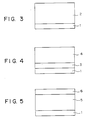
- the photosensitive material for electrophotography comprises an electrically conducting substrate 1 on which a single photosensitive layer 2 is provided containing the charge-generating agent and the charge-transporting agent therein.
- the layer 2 of generating and transporting the electric charge comprises a composition of a continuous phase which contains the charge-transporting agent (CTM) and a dispersion phase of a particular charge-generating agent (CGM) that is dispersed in the continuous phase as will be described later in detail.
- CTM charge-transporting agent
- CGM charge-generating agent
- another photosensitive material for electrophotography comprises an electrically conducting substrate 1 on which are provided a charge-generating layer (CGL) containing a particular charge-generating agent that will be described below in detail and a charge-transporting layer (CTL) 4 in the order mentioned.
- CGL charge-generating layer
- CTL charge-transporting layer
- a further photosensitive material for electrophotography comprises an electrically conducting substrate 1 on which are provided a charge-transporting layer (CTL) and a charge-generating layer (CGL) containing a particular charge-generating agent that will be mentioned below in detail in the order mentioned.
- CTL charge-transporting layer
- CGL charge-generating layer
- the photosensitive layer 2, the charge-transporting layer 4 or the charge-transporting agent (CTM) in the layer 5 may comprise a positive hole-transporting agent, an electron-transporting agent, or a combination thereof.
- the photosensitive material of the present invention may be provided, as an uppermost layer, with a protection layer that has been known per se. such as the one which contains, for example, a charge-transporting agent/or the electrically conducting fine powder.
- the P-type charge-generating grains and the N-type charge-generating grains are used in combination as a charge-generating agent, and at least part of them are made present in the form of aggregates in the photosensitive layer.
- Each aggregate comprises a plurality of the P-type (or the N-type) charge-generating grains which are aggregated together via the N-type (or the P-type) charge-generating grains of the contrasting polarity, and numerous P-N junctions exist in the aggregates.
- These pigments have a porphyrin skeleton represented by the following formula (1), wherein R1 and R2 form a benzene ring or naphthalene ring together with carbon atoms bonded thereto.
- the P-type charge-generating pigment usually has a grain size of from 0.1 to 1 ⁇ m.
- N-type charge-generating grains that constitute aggregates there can be used a known N-type charge-generating pigment such as perylene pigment, azo pigment, squalillium salt pigment or polycyclic quinone pigment. There can be further used an N-type semiconductor or photoconductor in addition to the above.
- a known N-type charge-generating pigment such as perylene pigment, azo pigment, squalillium salt pigment or polycyclic quinone pigment.
- N-type semiconductor or photoconductor in addition to the above.
- the perylene pigment will have the following formula (2), wherein R2 and R4 are each a substituted or unsubstituted alkyl group with not more than 18 carbon atoms, a cycloalkyl group, an aryl group, or an aralkyl group, and the substituent may be an alkoxy group, a halogen atom or the like.
- any charge-generating pigment that has heretofore been used can be used such as monoazo pigment, disazo pigment or trisazo pigment.
- the squalillium salt pigment will have the following formula (3), wherein R5 and R6 are each an alkyl group, an alkoxy group, or a halogen atom, R7, R8, R9 and R10 are each an alkyl group, a cycloalkyl group, an alkoxy group, a halogen atom, an aryl group, or an aralkyl group, and each of the groups may have an alkyl group, an alkoxy group or a halogen atom as a substituent.
- polycyclic quinone pigment there can be used anthanthrone pigment, quinacridone pigment, perynone pigment, quinophthalone pigment, flavanthrone pigment, pyranthrone pigment, violanthrone pigment, anthrone pigment or indanthrone pigment,
- the above-mentioned N-type charge-generating pigment usually has a primary grain size of from 0.1 to ⁇ m.
- the P-type charge-generating pigment and the N-type charge-generating pigment should be used in amounts of a ratio of from 10:0.1 to 0.1:10 and, particularly, from 10:0.5 to 0.5:10.
- the N-type inorganic semiconductor or photoconductor there is usually used a semiconductor or a photoconductor of the type of an inorganic oxide.
- Preferred examples include, titanium oxide (TiO 2 ), tin oxide (SnO 2 ), indium-doped tin oxide (ITO), antimony-doped tin oxide and zinc oxide (ZnO).
- the inorganic semiconductor or photoconductor should usually be in a fine particular form having a primary grain size of from 0.01 to 5 ⁇ m and, particularly, from 0.1 to 1 ⁇ m.
- the ratio A:B should be from 10:1 to 1:40 and, particularly, from 2:1 to 6:40.
- the ratio of the inorganic semiconductor or photoconductor is greater than the above range, the charging property of the photosensitive layer tends to decrease.
- the ratio thereof is smaller than the above range, on the other hand, the sensitivity is not much improved and the abrasion resistance is not sufficiently improved, either.
- aggregates of the P-type charge-generating grains and the N-type charge-generating grains are not formed by simply dispersing them together in a resin solution, and a pretreatment must be carried out.
- the pretreatment can be by either a wet method or a dry method.
- the P-type charge-generating grains and the N-type charge-generating grains are dispersed in a finely pulverized form in a particular polar solvent such as a tetrahydrofurane or a dichloromethane to form aggregates thereof.
- the two grains are finely pulverized and are dispersed, so that the P-type charge-generating grains are positively charged and the N-type charge-generating grains are negatively charged to effectively form aggregates.
- the present inventors have confirmed through experiments the fact that even when the grains are mixed together in an organic solvent, the individual grains are not stably dispersed and the efficiency for forming aggregates strikingly decreases when there is used an alcohol, cyclohexane, toluene or dioxane.
- the aggregates can be effectively formed by effecting the wet pulverization using a ball mill, a colloid mill, a disperse mill or a homo mixer.
- the P-type charge-generating grains and the N-type charge-generating grains are mixed together and are pulverized together. Even by the mechano-chemical method, the grains are ground into primary grains which then aggregate together, so that aggregates grow.
- the pulverization is carried out using a ball mill and a vibration mill together.
- the P-type charge-generating grains and the N-type charge-generating grains can be used in amounts of the above-mentioned ratio.
- the photosensitive material of the positively charged type the photosensitive material should advantageously be comprised chiefly of the N-type charge-generating grains.
- the photosensitive material should advantageously be comprised chiefly of the P-type charge-generating grains.
- the aggregates By blending the N-type charge-generating grains in small amounts, improved balance is obtained in the spectral sensitivity and the sensitivity can be increased on the side of long wavelengths.
- the grains of the side of the larger amount may exist in the form of individual grains liberated from the aggregates.
- the presence of such free grains does not adversely affect the sensitivity.
- the aggregates used in the present invention are made up of a plurality of the P-type (N-type) charge-generating grains that are aggregated together via the N-type (P-type) charge-generating grains, and should have a grain size of from 0.2 to 2 ⁇ m.
- the sensitivity and electrically charging performance of the photosensitive material tend to decrease. This is attributed to that the central grains in the aggregates are concealed and that the light-receiving areas decrease. It is further considered that the presence of giant grains permits the electric charge to leak in the photosensitive layer, which causes the electrically charging performance to decrease.
- aggregates of the P-type and N-type charge-generating grains and the charge-transporting agent are dispersed in a solution of a binder resin for forming the photosensitive layer, and this coating composition is provided on the electrically conducting substrate to obtain a single-layer photosensitive material.
- the coating solution is prepared by a known method using, for example, a roll mill, a ball mill, an attritor, a paint shaker or an ultrasonic dispersing machine, and is then applied using a widely known coating means, followed by drying.
- the charge-transporting agent there can be used any known electron-transporting agent or positive hole-transporting agent, such as the compounds exemplified below. These charge-transporting agents can be used in a single kind or in a combination of a plurality of kinds. For instance, the electron-transporting agent can be used in combination with a small amount of the positive hole-transporting agent or, conversely, the positive hole-transporting agent can be used in combination with a small amount of the electron-transporting agent.
- Preferred examples of the electron-transporting agent include:
- Preferred examples of the positive hole-transporting agent include:
- a variety of resins can be used as a resin medium for dispersing the electron-transporting agent and the electron-generating agent.
- a variety of polymers like olefin polymers such as styrene polymer, acrylic polymer, styrene-acrylic polymer, ethylene-vinyl acetate copolymer, polypropylene, and ionomer, as well as photocuring resins such as polyvinyl chloride, vinyl chloride-vinyl acetate copolymer, polyester, alkyd resin, polyamide, polyurethane, epoxy resin, polycarbonate, polyallylate, polysulfone, diallyl phthalate resin, silicone resin, ketone resin, polyvinyl butylal resin, polyether resin, phenol resin and epoxy acrylate resin.
- olefin polymers such as styrene polymer, acrylic polymer, styrene-acrylic polymer, ethylene-vinyl acetate copolymer, poly
- binder resins can be used in a single kind or being mixed in two or more kinds.
- Preferred resins are styrene polymer, acrylic polymer, styrene-acrylic polymer, polyester, alkyd resin, polycarbonate and polyallylate.
- organic solvents can be used for forming the coating solution.
- examples thereof include alcohols such as methanol, ethanol, isopropanol and butanol, aliphatic hydrocarbons such as n-hexane, octane and cyclohexane, aromatic hydrocarbons such as benzene, toluene and xylene, halogenated hydrocarbons such as dichloromethane, dichloroethane, carbon tetrachloride and chlorobenzene, ethers such as dimethyl ether, diethyl ether, tetrahydrofurane, ethylene glycol dimethyl ether, and diethylene glycol dimethyl ether, ketones such as acetone, methyl ethyl ketone and cyclohexanone, esters such as ethyl acetate and methyl acetate, as well as dimethyl formamide and dimethyl sulfoxide, which can be used in a single kind or being mixed in two
- the charge-generating agent composed of the aforementioned grains should occupy from 75 to 1% by weight and, particularly, from 20 to 3% by weight of the whole amount on the basis of dry weight.
- the charge-transporting agent should be contained in an amount of from 80 to 10% by weight and, particularly, from 60 to 30% by weight of the whole amount.
- the coating solution should have a solid component concentration of generally from 5 to 50% by weight.
- composition for forming the photosensitive material of the present invention may be blended with a variety of widely known blending agents such as antioxidizing agent, radical scavenger, singlet quencher, UV-absorbing agent, softening agent, surface-reforming agent, defoaming agent, filler, viscosity-imparting agent, dispersion stabilizer, wax, acceptor, and donor.
- blending agents such as antioxidizing agent, radical scavenger, singlet quencher, UV-absorbing agent, softening agent, surface-reforming agent, defoaming agent, filler, viscosity-imparting agent, dispersion stabilizer, wax, acceptor, and donor.
- a variety of materials having electrically conducting property can be used as an electrically conducting substrate on which the photosensitive layer is to be provided.
- Examples include metals such as aluminum, copper, tin, platinum, gold, silver, vanadium, molybdenum, chromium, cadmium, titanium, nickel, indium, stainless steel and brass, as well as a plastic material on which the above-mentioned metals are deposited or laminated, and a glass covered with aluminum iodide, tin oxide or indium oxide.
- the photosensitive layer of the single dispersion type should, generally, have a thickness of from 5 to 100 ⁇ m and, particularly, from 10 to 50 ⁇ m.
- the thickness is smaller than the above range, the surface potential tends to decrease and when the thickness is larger than the above range, on the other hand, the sensitivity decreases and the residual potential increases.
- the photosensitive material shown in Fig. 4 has the charge-generating layer provided on the electrically conducting substrate.
- the coating composition for forming the charge-generating layer is obtained by dispersing the charge-generating agent in the aforementioned resin solution, and should contain the charge-generating agent in an amount of from 99 to 1% by weight and, particularly, from 80 to 50% by weight reckoned as solid components, and should further have a thickness of from 0.01 to ⁇ m and, particularly, from 0.1 to 5 ⁇ m.
- the charge-transporting layer is provided on the charge-generating layer.
- the charge-transporting layer is obtained by dispersing the above-mentioned charge-transporting agent in the above-mentioned resin solution, and should contain a derivative in an amount of from 80 to 10% by weight and, particularly, from 60 to 30% by weight per the total solid components of the two, and should further have a thickness of from 1 to 100 ⁇ m and, particularly, from 5 to 50 ⁇ m.
- the charge-transporting agent in the charge-generating agent should be chiefly comprised of an electron-transporting agent and for the negatively charging applications, the charge-transporting agent in the charge-generating agent should be chiefly comprised of a positive hole-transporting agent.
- the photosensitive material shown in Fig. 5 has the charge-transporting layer provided on the electrically conducting substrate, and further has the charge-generating layer provided thereon.
- the compositions and thicknesses of the charge-transporting layer and of the charge-generating layer may be the same as those of the aforementioned case.
- the sheet-like photosensitive materials for electrophotography prepared in Examples and Comparative Examples were subjected to the charging step in which the flow of current was adjusted as described above, to the exposure step (same as described above but without using interference filter); and to the discharging step (irradiated with white light of 1000 lux for one second) a hundred times repetitively using the above-mentioned electrostatic copy testing apparatus (EPA-8100 manufactured by Kawaguchi Denki Co.). Thereafter, the surface potential SP100 (V) and the residual potential RP(100 (V) were measured in the same manner as described above, and differences from the initial surface potential and the initial residual potential were calculated by using the following formulas.
- ⁇ SP (SP100) - (SP1)
- ⁇ RP (RP100) - (RP1)
- a perylene pigment of the following formula (4) and an X-type metal-free phthalocyanine of the following formula (5) were pre-dispersed at a ratio of 10 parts by weight to one part by weight in 100 parts by weight of the THF for one hour using a ball mill, to which were then added 50 parts by weight of an N,N-diethylamino-p-benzaldehyde diphenylhydrazone (DEH; compound of the formula (6)) as a charge-transporting agent and 100 parts by weight of a polycarbonate (produced by Mitsubishi Gas Kagaku Co.) as a binder resin.
- DEH N,N-diethylamino-p-benzaldehyde diphenylhydrazone
- the mixture was then homogeneously dispersed for one hour using the ball mill to prepare a coating solution which was then heat-treated at 120 °C for one hour, and was applied onto an aluminum substrate (sheet) such that the film thickness was 20 ⁇ m (grain size of aggregates: 0.2 to 2 ⁇ m).
- the dispersion structure in the photosensitive layer was as shown in Fig. 1.
- Aggregates (grain size of aggregates: 0.2 to 2 ⁇ m) were formed in the same manner as in Example 1 but using an azo pigment (compound of the following formula (7)) instead of the perylene pigment, and a photosensitive material was formed in the same manner as in Example 1.
- Aggregates (grain size of aggregates: 0.2 to 2 ⁇ m) were formed in the same manner as in Example 1 but using an a polycyclic quinone pigment (compound of the following formula (8)) instead of the perylene pigment, and a photosensitive material was formed in the same manner as in Example 1.
- Aggregates (grain size of aggregates: 0.2 to 2 ⁇ m) were formed in the same manner as in Example 1 but using an a naphthalocyanine (compound of the following formula (9)) instead of the X-type metal-free phthalocyanine, and a photosensitive material was formed in the same manner as in Example 1.
- a naphthalocyanine compound of the following formula (9)
- Aggregates (grain size of aggregates: 0.2 to 2 ⁇ m) were formed in the same manner as in Example 1 but using the perylene pigment and the X-type metal-free phthalocyanine at a ratio of 10 parts by weight to 3 parts by weight, and a photosensitive material was formed in the same manner as in Example 1.
- Aggregates (grain size of aggregates: 0.2 to 2 ⁇ m) were formed in the same manner as in Example 1 but using the perylene pigment and the X-type metal-free phthalocyanine at a ratio of 10 parts by weight to 0.2 parts by weight, and a photosensitive material was formed in the same manner as in Example 1.
- Aggregates (grain size of aggregates: 0.2 to 2 ⁇ m) were formed in the same manner as in Example 1 but dispersing the perylene pigment and the X-type metal-free phthalocyanine in the THF for 100 hours using the ball mill, and a photosensitive material was formed in the same manner as in Example 1.
- a photosensitive material was formed in the same manner as in Example 1 but using the perylene pigment alone in an amount of 10 parts by weight.
- a photosensitive material was formed in the same manner as in Example 1 but using the X-type metal-free phthalocyanine alone in an amount of 1 part by weight.
- a photosensitive material was formed in the same manner as in Example 1 but using the X-type metal-free phthalocyanine alone in an amount of 10 parts by weight.
- a photosensitive material was formed in the same manner as in Example 1 but dispersing the perylene pigment and the X-type metal-free phthalocyanine together with the charge-transporting agent and the binder resin without pretreatment.
- the dispersion structure of this photosensitive layer was as shown in Fig. 2, from which formation of aggregates was not recognized.
- a photosensitive material was formed in the same manner as in Example 1 but by dispersing the perylene pigment and the X-type metal-free phthalocyanine for 5 minutes using a ball mill as the pretreatment.
- a photosensitive material was formed in the same manner as in Example 1 but using toluene for pre-treating the perylene pigment and the X-type metal-free phthalocyanine.
- a photosensitive material was formed in the same manner as in Example 1 but using benzene for pre-dispersing the perylene pigment and the X-type metal-free phthalocyanine.
- a photosensitive material was formed in the same manner as in Comparative Example 4 but using the perylene pigment and the X-type metal-free phthalocyanine each in an amount of 10 parts by weight.
- Example 1 2.1 was not halved 81 1 30 -11 +15 Comp.
- Example 2 was not halved ditto 1 15 20 - - Comp.
- Example 3 ditto 5.0 1 73 28 - +20 Comp.
- Example 4 2.1 was not halved 80 15 32 -25 +20 Comp.
- Example 5 2.1 ditto 81 16 31 -10 + 8 Comp.
- Example 6 2.1 ditto 81 15 30 -10 + 9 Comp.
- Example 7 2.1 ditto 81 15 30 -10 + 8 Comp.
- Example 8 3.2 8.9 135 64 43 -120 +56
- An X-type metal-free phthalocyanine and TiO 2 were dispersed at a ratio of 10 parts by weight to one part by weight in 100 parts by weight of the THF for one hour using a ball mill, to which were then added 50 parts by weight of the DEH as a charge-transporting agent and 100 parts by weight of a polycarbonate (produced by Mitsubishi Gas Kagaku Co.) as a binder resin.
- the mixture was then homogeneously dispersed for one hour using the ball mill to prepare a coating solution which was then heat-treated at 120 °C for one hour, and was applied onto an aluminum substrate (sheet) such that the film thickness was 20 ⁇ m.
- a photosensitive material was formed in the same manner as in Example 1 but using TiO 2 in an amount of 10 parts by weight.
- a photosensitive material was formed in the same manner as in Example 1 but using TiO 2 in an amount of 40 parts by weight.
- a photosensitive material was formed in the same manner as in Example 1 but using SnO 2 instead of TiO 2 .
- a photosensitive material was formed in the same manner as in Example 1 but using antimony-doped tin oxide (SnSb x O 2 ) instead of TiO 2 .
- SnSb x O 2 antimony-doped tin oxide
- a photosensitive material was formed in the same manner as in Example 1 but using indium-doped tin oxide (SnIn X O 2 ) instead of TiO 2 .
- a photosensitive material was formed in the same manner as in Example 8 without using X-type metal-free phthalocyanine but using TiO 2 in an amount of 50 parts by weight.
- a photosensitive material was formed in the same manner as in Example 8 without using X-type metal-free phthalocyanine but using TiO 2 in an amount of 0.1 parts by weight.
- Photosensitive materials obtained in Examples 8 to 13 and in Comparative Examples 3, 9 and 10 were evaluated for their properties and abrasion resistance in the same manner as in Example 1. The results were as shown in Table 2. The abrasion resistance was evaluated by measuring a difference between the initial thickness of the photosensitive layer and the thickness of the photosensitive layer after the copying operation was repeated 1000 times by using a printer (LDC-630, produced by Mita Kogyo Co.).
- the photosensitive material of the present invention exhibits very high sensitivity and excellent surface abrasion resistance.
- N-type inorganic semiconductor or photoconductor (TiO 2 in Table 2) that is added in an increased amount makes it possible to improve not only the charge generation efficiency but also the charge-transporting efficiency and sensitivity.
Landscapes
- Physics & Mathematics (AREA)
- General Physics & Mathematics (AREA)
- Chemical & Material Sciences (AREA)
- Inorganic Chemistry (AREA)
- Photoreceptors In Electrophotography (AREA)
Claims (8)
- Lichtempfindliches Material für die Elektrophotographie, mit einem elektrisch leitenden Substrat und einer lichtempfindlichen Harzschicht, die ein ladungserzeugendes Mittel und ein ladungstransportierendes Mittel enthält, wobei das ladungserzeugende Mittel ein Aggregat aus (i) einem ladungserzeugenden Pigment des P-Typs, das ein metallfreies Phthalocyanin des X-Typs, ein Oxotitanylphthalocyanin oder ein metall freies Naphthalocyanin ist, und (ii) entweder einem ladungserzeugenden Pigment des N-Typs oder einem anorganischen Halbleiter oder Photoleiter des N-Typs enthält, wobei das Aggregat eine Korngröße von 0,2 bis 2 µm aufweist und in eine lichtempfindliche Harzschicht dispergiert ist.
- Lichtempfindliches Material nach Anspruch 1, das ein ladungserzeugendes Pigment des N-Typs enthält, das aus Perylen-Pigmenten, Azo-Pigmenten, SqualilliumsalzPigmenten und polyzyklischen Chinon-Pigmenten gewählt ist.
- Lichtempfindliches Material nach Anspruch 1 oder 2, das ein ladungserzeugendes Pigment des P-Typs und ein ladungserzeugendes Pigment des N-Typs in einem Gewichtsverhältnis von 10:0,1 bis 0,1:10 enthält.
- Lichtempfindliches Material nach Anspruch 1 oder Anspruch 2, das ein organisches ladungserzeugendes Pigment des P-Typs und einen anorganischen Halbleiter oder Photoleiter des N-Typs in einem Gewichtsverhältnis von 10:1 bis 1:40 enthält.
- Lichtempfindliches Material nach Anspruch 4, in dem der anorganische Halbleiter oder Photoleiter des N-Typs ein Pigment ist, das aus Titandioxid, Zinnoxid, mit Antimon dotiertem oder mit Indium dotiertem Zinnoxid und Zinkoxid gewählt wird.
- Lichtempfindliches Material nach irgendeinem der Ansprüche 1 bis 5, in dem das ladungserzeugende Pigment des P-Typs und das ladungserzeugende Pigment des N-Typs oder der anorganische Halbleiter oder Photoleiter des N-Typs jeweils eine Korngröße von 0,1 bis 1 µm aufweisen.
- Lichtempfindliches Material nach irgendeinem der Ansprüche 1 bis 6, in dem die lichtempfindliche Schicht eine lichtempfindliche Schicht des Einzeldispersionstyps ist, die das ladungserzeugende Mittel und das ladungstransportierende Mittel enthält.
- Verwendung eines lichtempfindlichen Materials gemäß irgendeinem der Ansprüche 1 bis 7 in der Elektrophotographie.
Applications Claiming Priority (4)
| Application Number | Priority Date | Filing Date | Title |
|---|---|---|---|
| JP15970093 | 1993-06-29 | ||
| JP159700/93 | 1993-06-29 | ||
| JP5152294A JPH07261413A (ja) | 1994-03-23 | 1994-03-23 | 電子写真感光体 |
| JP51522/94 | 1994-03-23 |
Publications (2)
| Publication Number | Publication Date |
|---|---|
| EP0632332A1 EP0632332A1 (de) | 1995-01-04 |
| EP0632332B1 true EP0632332B1 (de) | 1997-01-15 |
Family
ID=26392070
Family Applications (1)
| Application Number | Title | Priority Date | Filing Date |
|---|---|---|---|
| EP94304709A Expired - Lifetime EP0632332B1 (de) | 1993-06-29 | 1994-06-28 | Photoempfindliches Material für die Elektrophotographie |
Country Status (3)
| Country | Link |
|---|---|
| US (2) | US5656407A (de) |
| EP (1) | EP0632332B1 (de) |
| DE (1) | DE69401466T2 (de) |
Families Citing this family (47)
| Publication number | Priority date | Publication date | Assignee | Title |
|---|---|---|---|---|
| US5656407A (en) * | 1993-06-29 | 1997-08-12 | Mita Industrial Co., Ltd. | Photosensitive material for electrophotography |
| US5895739A (en) * | 1997-11-25 | 1999-04-20 | Lexmark International, Inc. | Enhanced photoconductive oxo-titanyl phthalocyanine |
| US6022657A (en) * | 1998-12-22 | 2000-02-08 | Lexmark International, Inc. | Methods of making charge generation layers containing charge transport compound, and photoconductors containing the same |
| US6136483A (en) * | 1998-08-27 | 2000-10-24 | Ricoh Company, Ltd. | Electrophotographic photoconductor and electrophotographic image forming apparatus using the photoconductor |
| JP3464407B2 (ja) * | 1999-04-12 | 2003-11-10 | シャープ株式会社 | 電子写真感光体およびその製造方法 |
| JP3522604B2 (ja) | 1999-09-03 | 2004-04-26 | シャープ株式会社 | 電子写真感光体 |
| US6218062B1 (en) | 1999-10-12 | 2001-04-17 | Xerox Corporation | Charge generating layer with needle shaped particles |
| US6177219B1 (en) | 1999-10-12 | 2001-01-23 | Xerox Corporation | Blocking layer with needle shaped particles |
| US6200716B1 (en) | 1999-11-15 | 2001-03-13 | Xerox Corporation | Photoreceptor with poly (vinylbenzyl alcohol) |
| JP3357030B2 (ja) * | 2000-09-01 | 2002-12-16 | 科学技術振興事業団 | 樹脂分散有機半導体膜を用いた増倍素子 |
| US7244485B2 (en) * | 2001-04-11 | 2007-07-17 | Xerox Corporation | Imageable seamed belts having polyamide adhesive between interlocking seaming members |
| US6683175B2 (en) * | 2001-04-12 | 2004-01-27 | Canon Kabushiki Kaisha | Porphyrin compound, and electrophotographic photosensitive member, process-cartridge and apparatus using the compound |
| JP2003015334A (ja) * | 2001-04-27 | 2003-01-17 | Fuji Denki Gazo Device Kk | 電子写真用感光体およびその製造方法 |
| JP2004117558A (ja) * | 2002-09-24 | 2004-04-15 | Kyocera Mita Corp | 単層型電子写真感光体 |
| JP4082153B2 (ja) * | 2002-09-27 | 2008-04-30 | コニカミノルタホールディングス株式会社 | 画像形成方法及び画像形成装置 |
| JP4767523B2 (ja) * | 2004-07-05 | 2011-09-07 | 株式会社リコー | 電子写真感光体、それを用いた画像形成方法、画像形成装置及び画像形成装置用プロセスカートリッジ |
| US7462433B2 (en) * | 2005-08-26 | 2008-12-09 | Xerox Corporation | Photoreceptor additive |
| US7427462B2 (en) * | 2005-09-01 | 2008-09-23 | Xerox Corporation | Photoreceptor layer having rhodamine additive |
| US20070077505A1 (en) * | 2005-10-04 | 2007-04-05 | Xerox Corporation | Imaging member |
| US7544453B2 (en) * | 2005-10-11 | 2009-06-09 | Xerox Corporation | Photoreceptor with improved electron transport |
| US7399565B2 (en) * | 2005-10-24 | 2008-07-15 | Xerox Corporation | Imaging member having undercoat layer comprising porphine additive |
| US7527904B2 (en) * | 2005-12-19 | 2009-05-05 | Xerox Corporation | Imaging member |
| US7419752B2 (en) * | 2006-03-20 | 2008-09-02 | Xerox Corporation | Imaging member having polyvinylidene chloride barrier polymer resins |
| US7604914B2 (en) * | 2006-04-13 | 2009-10-20 | Xerox Corporation | Imaging member |
| US20070248813A1 (en) * | 2006-04-25 | 2007-10-25 | Xerox Corporation | Imaging member having styrene |
| EP1884544B1 (de) * | 2006-07-31 | 2011-09-07 | Kyocera Mita Corporation | Oxotitanylphthalocyaninkristall, Herstellungsverfahren dafür und elektrographischer Photorezeptor |
| US8048601B2 (en) | 2008-05-30 | 2011-11-01 | Xerox Corporation | Aminosilane and self crosslinking acrylic resin hole blocking layer photoconductors |
| US8062816B2 (en) | 2008-05-30 | 2011-11-22 | Xerox Corporation | Phosphonate hole blocking layer photoconductors |
| US8098925B2 (en) * | 2008-11-12 | 2012-01-17 | Xerox Corporation | Photoconductors and processes thereof |
| US7811730B2 (en) * | 2008-12-11 | 2010-10-12 | Xerox Corporation | Imaging member |
| US7811729B2 (en) * | 2008-12-11 | 2010-10-12 | Xerox Corporation | Imaging member |
| US7943276B2 (en) * | 2008-12-11 | 2011-05-17 | Xerox Corporation | Imaging member |
| US8057974B2 (en) * | 2008-12-11 | 2011-11-15 | Xerox Corporation | Imaging member |
| US8409773B2 (en) | 2009-02-27 | 2013-04-02 | Xerox Corporation | Epoxy carboxyl resin mixture hole blocking layer photoconductors |
| US8278015B2 (en) * | 2009-04-15 | 2012-10-02 | Xerox Corporation | Charge transport layer comprising anti-oxidants |
| US7799140B1 (en) | 2009-06-17 | 2010-09-21 | Xerox Corporation | Process for the removal of photoreceptor coatings using a stripping solution |
| US8142968B2 (en) * | 2009-06-17 | 2012-03-27 | Xerox Corporation | Photoreceptor with release layer |
| US20110014556A1 (en) * | 2009-07-20 | 2011-01-20 | Xerox Corporation | Charge acceptance stabilizer containing charge transport layer |
| US8361685B2 (en) * | 2009-11-05 | 2013-01-29 | Xerox Corporation | Silane release layer and methods for using the same |
| US8372568B2 (en) * | 2009-11-05 | 2013-02-12 | Xerox Corporation | Gelatin release layer and methods for using the same |
| US8304151B2 (en) * | 2009-11-30 | 2012-11-06 | Xerox Corporation | Corona and wear resistant imaging member |
| US8257892B2 (en) * | 2010-01-22 | 2012-09-04 | Xerox Corporation | Releasable undercoat layer and methods for using the same |
| US20110180099A1 (en) * | 2010-01-22 | 2011-07-28 | Xerox Corporation | Releasable undercoat layer and methods for using the same |
| US8481235B2 (en) | 2010-08-26 | 2013-07-09 | Xerox Corporation | Pentanediol ester containing photoconductors |
| US8426092B2 (en) | 2010-08-26 | 2013-04-23 | Xerox Corporation | Poly(imide-carbonate) polytetrafluoroethylene containing photoconductors |
| JP5814212B2 (ja) | 2012-10-31 | 2015-11-17 | 京セラドキュメントソリューションズ株式会社 | 電子写真感光体及び画像形成装置 |
| US9529286B2 (en) | 2013-10-11 | 2016-12-27 | Xerox Corporation | Antioxidants for overcoat layers and methods for making the same |
Family Cites Families (15)
| Publication number | Priority date | Publication date | Assignee | Title |
|---|---|---|---|---|
| DE2353639C2 (de) * | 1973-10-26 | 1983-08-04 | Hoechst Ag, 6230 Frankfurt | Elektrophotographisches Aufzeichnungsmaterial |
| JPS59116753A (ja) * | 1982-12-24 | 1984-07-05 | Toyo Ink Mfg Co Ltd | 電子写真感光体 |
| JPS6318353A (ja) * | 1986-07-10 | 1988-01-26 | Toppan Printing Co Ltd | 電子写真感光体 |
| JPS63220161A (ja) * | 1987-03-10 | 1988-09-13 | Canon Inc | 電子写真感光体 |
| US4877702A (en) * | 1987-10-30 | 1989-10-31 | Mita Industrial Co., Ltd. | Electrophotographic sensitive material |
| JPH01177553A (ja) * | 1988-01-07 | 1989-07-13 | Fuji Xerox Co Ltd | 電子写真用感光体 |
| US4882254A (en) * | 1988-07-05 | 1989-11-21 | Xerox Corporation | Photoconductive imaging members with mixtures of photogenerator pigment compositions |
| EP0369765B1 (de) * | 1988-11-16 | 1995-01-25 | Mita Industrial Co. Ltd. | Elektrophotographisches lichtempfindliches Material |
| KR0134186B1 (ko) * | 1989-02-28 | 1998-04-29 | 미타 요시히로 | 전자사진 감광체 |
| GB2231166B (en) * | 1989-04-13 | 1993-05-05 | Ind Tech Res Inst | Organic photoreceptor for use in electrophotography |
| US5328788A (en) * | 1990-07-26 | 1994-07-12 | Matsushita Electric Industrial Co., Ltd. | Organic photoconductive material for electrophotography and method for making the same |
| JPH04275556A (ja) * | 1990-12-17 | 1992-10-01 | Eastman Kodak Co | 近赤外線感光性の光導電性素子 |
| JPH05232724A (ja) * | 1992-02-21 | 1993-09-10 | Matsushita Electric Ind Co Ltd | 電子写真用感光体 |
| JPH05333575A (ja) * | 1992-06-01 | 1993-12-17 | Hitachi Ltd | 電子写真感光体 |
| US5656407A (en) * | 1993-06-29 | 1997-08-12 | Mita Industrial Co., Ltd. | Photosensitive material for electrophotography |
-
1994
- 1994-06-27 US US08/266,503 patent/US5656407A/en not_active Expired - Lifetime
- 1994-06-28 EP EP94304709A patent/EP0632332B1/de not_active Expired - Lifetime
- 1994-06-28 DE DE69401466T patent/DE69401466T2/de not_active Expired - Lifetime
-
1997
- 1997-01-30 US US08/791,405 patent/US5821021A/en not_active Expired - Lifetime
Also Published As
| Publication number | Publication date |
|---|---|
| DE69401466D1 (de) | 1997-02-27 |
| US5656407A (en) | 1997-08-12 |
| DE69401466T2 (de) | 1997-07-24 |
| US5821021A (en) | 1998-10-13 |
| EP0632332A1 (de) | 1995-01-04 |
Similar Documents
| Publication | Publication Date | Title |
|---|---|---|
| EP0632332B1 (de) | Photoempfindliches Material für die Elektrophotographie | |
| JP2732697B2 (ja) | 両帯電可能な電子写真用有機感光体 | |
| EP0707245B1 (de) | Elektrophotographisches Verfahren | |
| EP0810481B1 (de) | Elektrophotographischer Photorezeptor | |
| JP3176797B2 (ja) | 電子写真用感光体 | |
| JPH061385B2 (ja) | 電子写真感光体 | |
| JP3606469B2 (ja) | 光導電性組成物の製造方法及びこの光導電性組成物を用いる電子写真用感光体の製造方法 | |
| JPS63271455A (ja) | 有機感光体 | |
| JPH07261413A (ja) | 電子写真感光体 | |
| JP2573222B2 (ja) | 有機感光体 | |
| JP2001159838A (ja) | 電子写真画像形成装置 | |
| EP0709747B1 (de) | Entwicklungsvorspannungsauswahl zur Verwendung in einem elektrofotografischem Verfahren, welches fotoempfindliches Material verwendet | |
| JPH0520742B2 (de) | ||
| JP3482484B2 (ja) | 顔料混合物、その製造方法、その顔料混合物を含有する感光層塗工液、及びその顔料混合物を含有する電子写真感光体 | |
| JP2000019747A (ja) | 負帯電単層型電子写真感光体 | |
| JP3585427B2 (ja) | 画像形成装置 | |
| JPH0520745B2 (de) | ||
| JP2833192B2 (ja) | 電子写真用感光体 | |
| JP2518834B2 (ja) | 電子写真感光体用電荷発生材料 | |
| JPS63271452A (ja) | 有機感光体 | |
| JPH0520744B2 (de) | ||
| JPH07319182A (ja) | 電子写真用感光体 | |
| JPH07114195A (ja) | 電子写真感光体 | |
| JP2000047406A (ja) | 光導電体、有機顔料分散液及びそれを用いた光導電体の製造方法、及び電子写真方法及び電子写真装置 | |
| JPH07239561A (ja) | 電子写真用感光体 |
Legal Events
| Date | Code | Title | Description |
|---|---|---|---|
| PUAI | Public reference made under article 153(3) epc to a published international application that has entered the european phase |
Free format text: ORIGINAL CODE: 0009012 |
|
| AK | Designated contracting states |
Kind code of ref document: A1 Designated state(s): DE FR GB IT |
|
| 17P | Request for examination filed |
Effective date: 19950208 |
|
| 17Q | First examination report despatched |
Effective date: 19950412 |
|
| GRAG | Despatch of communication of intention to grant |
Free format text: ORIGINAL CODE: EPIDOS AGRA |
|
| GRAH | Despatch of communication of intention to grant a patent |
Free format text: ORIGINAL CODE: EPIDOS IGRA |
|
| GRAH | Despatch of communication of intention to grant a patent |
Free format text: ORIGINAL CODE: EPIDOS IGRA |
|
| GRAA | (expected) grant |
Free format text: ORIGINAL CODE: 0009210 |
|
| AK | Designated contracting states |
Kind code of ref document: B1 Designated state(s): DE FR GB IT |
|
| ET | Fr: translation filed | ||
| REF | Corresponds to: |
Ref document number: 69401466 Country of ref document: DE Date of ref document: 19970227 |
|
| ITF | It: translation for a ep patent filed | ||
| PLBE | No opposition filed within time limit |
Free format text: ORIGINAL CODE: 0009261 |
|
| STAA | Information on the status of an ep patent application or granted ep patent |
Free format text: STATUS: NO OPPOSITION FILED WITHIN TIME LIMIT |
|
| 26N | No opposition filed | ||
| PGFP | Annual fee paid to national office [announced via postgrant information from national office to epo] |
Ref country code: FR Payment date: 19980609 Year of fee payment: 5 |
|
| PG25 | Lapsed in a contracting state [announced via postgrant information from national office to epo] |
Ref country code: FR Free format text: THE PATENT HAS BEEN ANNULLED BY A DECISION OF A NATIONAL AUTHORITY Effective date: 19990630 |
|
| REG | Reference to a national code |
Ref country code: FR Ref legal event code: ST |
|
| REG | Reference to a national code |
Ref country code: GB Ref legal event code: IF02 |
|
| PG25 | Lapsed in a contracting state [announced via postgrant information from national office to epo] |
Ref country code: IT Free format text: LAPSE BECAUSE OF NON-PAYMENT OF DUE FEES Effective date: 20050628 |
|
| PGFP | Annual fee paid to national office [announced via postgrant information from national office to epo] |
Ref country code: DE Payment date: 20130626 Year of fee payment: 20 Ref country code: GB Payment date: 20130626 Year of fee payment: 20 |
|
| REG | Reference to a national code |
Ref country code: DE Ref legal event code: R071 Ref document number: 69401466 Country of ref document: DE |
|
| REG | Reference to a national code |
Ref country code: DE Ref legal event code: R071 Ref document number: 69401466 Country of ref document: DE |
|
| REG | Reference to a national code |
Ref country code: GB Ref legal event code: PE20 Expiry date: 20140627 |
|
| PG25 | Lapsed in a contracting state [announced via postgrant information from national office to epo] |
Ref country code: GB Free format text: LAPSE BECAUSE OF EXPIRATION OF PROTECTION Effective date: 20140627 |
|
| PG25 | Lapsed in a contracting state [announced via postgrant information from national office to epo] |
Ref country code: DE Free format text: LAPSE BECAUSE OF EXPIRATION OF PROTECTION Effective date: 20140701 |