EP0632486A2 - Epitaktischer Halbleitermaterial und Herstellungsverfahren - Google Patents
Epitaktischer Halbleitermaterial und Herstellungsverfahren Download PDFInfo
- Publication number
- EP0632486A2 EP0632486A2 EP94302800A EP94302800A EP0632486A2 EP 0632486 A2 EP0632486 A2 EP 0632486A2 EP 94302800 A EP94302800 A EP 94302800A EP 94302800 A EP94302800 A EP 94302800A EP 0632486 A2 EP0632486 A2 EP 0632486A2
- Authority
- EP
- European Patent Office
- Prior art keywords
- layer
- germanium
- region
- silicon
- misfit dislocations
- Prior art date
- Legal status (The legal status is an assumption and is not a legal conclusion. Google has not performed a legal analysis and makes no representation as to the accuracy of the status listed.)
- Granted
Links
Images


Classifications
-
- H—ELECTRICITY
- H10—SEMICONDUCTOR DEVICES; ELECTRIC SOLID-STATE DEVICES NOT OTHERWISE PROVIDED FOR
- H10D—INORGANIC ELECTRIC SEMICONDUCTOR DEVICES
- H10D48/00—Individual devices not covered by groups H10D1/00 - H10D44/00
- H10D48/30—Devices controlled by electric currents or voltages
- H10D48/32—Devices controlled by only the electric current supplied, or only the electric potential applied, to an electrode which does not carry the current to be rectified, amplified or switched
- H10D48/34—Bipolar devices
-
- H—ELECTRICITY
- H10—SEMICONDUCTOR DEVICES; ELECTRIC SOLID-STATE DEVICES NOT OTHERWISE PROVIDED FOR
- H10D—INORGANIC ELECTRIC SEMICONDUCTOR DEVICES
- H10D8/00—Diodes
- H10D8/01—Manufacture or treatment
- H10D8/045—Manufacture or treatment of PN junction diodes
-
- H—ELECTRICITY
- H10—SEMICONDUCTOR DEVICES; ELECTRIC SOLID-STATE DEVICES NOT OTHERWISE PROVIDED FOR
- H10D—INORGANIC ELECTRIC SEMICONDUCTOR DEVICES
- H10D62/00—Semiconductor bodies, or regions thereof, of devices having potential barriers
- H10D62/50—Physical imperfections
- H10D62/53—Physical imperfections the imperfections being within the semiconductor body
-
- H—ELECTRICITY
- H10—SEMICONDUCTOR DEVICES; ELECTRIC SOLID-STATE DEVICES NOT OTHERWISE PROVIDED FOR
- H10D—INORGANIC ELECTRIC SEMICONDUCTOR DEVICES
- H10D62/00—Semiconductor bodies, or regions thereof, of devices having potential barriers
- H10D62/80—Semiconductor bodies, or regions thereof, of devices having potential barriers characterised by the materials
- H10D62/82—Heterojunctions
- H10D62/822—Heterojunctions comprising only Group IV materials heterojunctions, e.g. Si/Ge heterojunctions
-
- H—ELECTRICITY
- H10—SEMICONDUCTOR DEVICES; ELECTRIC SOLID-STATE DEVICES NOT OTHERWISE PROVIDED FOR
- H10P—GENERIC PROCESSES OR APPARATUS FOR THE MANUFACTURE OR TREATMENT OF DEVICES COVERED BY CLASS H10
- H10P14/00—Formation of materials, e.g. in the shape of layers or pillars
- H10P14/20—Formation of materials, e.g. in the shape of layers or pillars of semiconductor materials
- H10P14/24—Formation of materials, e.g. in the shape of layers or pillars of semiconductor materials using chemical vapour deposition [CVD]
-
- H—ELECTRICITY
- H10—SEMICONDUCTOR DEVICES; ELECTRIC SOLID-STATE DEVICES NOT OTHERWISE PROVIDED FOR
- H10P—GENERIC PROCESSES OR APPARATUS FOR THE MANUFACTURE OR TREATMENT OF DEVICES COVERED BY CLASS H10
- H10P14/00—Formation of materials, e.g. in the shape of layers or pillars
- H10P14/20—Formation of materials, e.g. in the shape of layers or pillars of semiconductor materials
- H10P14/29—Formation of materials, e.g. in the shape of layers or pillars of semiconductor materials characterised by the substrates
- H10P14/2901—Materials
- H10P14/2902—Materials being Group IVA materials
- H10P14/2905—Silicon, silicon germanium or germanium
-
- H—ELECTRICITY
- H10—SEMICONDUCTOR DEVICES; ELECTRIC SOLID-STATE DEVICES NOT OTHERWISE PROVIDED FOR
- H10P—GENERIC PROCESSES OR APPARATUS FOR THE MANUFACTURE OR TREATMENT OF DEVICES COVERED BY CLASS H10
- H10P14/00—Formation of materials, e.g. in the shape of layers or pillars
- H10P14/20—Formation of materials, e.g. in the shape of layers or pillars of semiconductor materials
- H10P14/32—Formation of materials, e.g. in the shape of layers or pillars of semiconductor materials characterised by intermediate layers between substrates and deposited layers
- H10P14/3202—Materials thereof
- H10P14/3204—Materials thereof being Group IVA semiconducting materials
- H10P14/3211—Silicon, silicon germanium or germanium
-
- H—ELECTRICITY
- H10—SEMICONDUCTOR DEVICES; ELECTRIC SOLID-STATE DEVICES NOT OTHERWISE PROVIDED FOR
- H10P—GENERIC PROCESSES OR APPARATUS FOR THE MANUFACTURE OR TREATMENT OF DEVICES COVERED BY CLASS H10
- H10P14/00—Formation of materials, e.g. in the shape of layers or pillars
- H10P14/20—Formation of materials, e.g. in the shape of layers or pillars of semiconductor materials
- H10P14/32—Formation of materials, e.g. in the shape of layers or pillars of semiconductor materials characterised by intermediate layers between substrates and deposited layers
- H10P14/3242—Structure
- H10P14/3244—Layer structure
- H10P14/3251—Layer structure consisting of three or more layers
-
- H—ELECTRICITY
- H10—SEMICONDUCTOR DEVICES; ELECTRIC SOLID-STATE DEVICES NOT OTHERWISE PROVIDED FOR
- H10P—GENERIC PROCESSES OR APPARATUS FOR THE MANUFACTURE OR TREATMENT OF DEVICES COVERED BY CLASS H10
- H10P14/00—Formation of materials, e.g. in the shape of layers or pillars
- H10P14/20—Formation of materials, e.g. in the shape of layers or pillars of semiconductor materials
- H10P14/34—Deposited materials, e.g. layers
- H10P14/3402—Deposited materials, e.g. layers characterised by the chemical composition
- H10P14/3404—Deposited materials, e.g. layers characterised by the chemical composition being Group IVA materials
- H10P14/3411—Silicon, silicon germanium or germanium
-
- H—ELECTRICITY
- H10—SEMICONDUCTOR DEVICES; ELECTRIC SOLID-STATE DEVICES NOT OTHERWISE PROVIDED FOR
- H10P—GENERIC PROCESSES OR APPARATUS FOR THE MANUFACTURE OR TREATMENT OF DEVICES COVERED BY CLASS H10
- H10P32/00—Diffusion of dopants within, into or out of wafers, substrates or parts of devices
- H10P32/10—Diffusion of dopants within, into or out of semiconductor bodies or layers
- H10P32/17—Diffusion of dopants within, into or out of semiconductor bodies or layers characterised by the semiconductor material
- H10P32/171—Diffusion of dopants within, into or out of semiconductor bodies or layers characterised by the semiconductor material being group IV material
-
- H—ELECTRICITY
- H10—SEMICONDUCTOR DEVICES; ELECTRIC SOLID-STATE DEVICES NOT OTHERWISE PROVIDED FOR
- H10P—GENERIC PROCESSES OR APPARATUS FOR THE MANUFACTURE OR TREATMENT OF DEVICES COVERED BY CLASS H10
- H10P32/00—Diffusion of dopants within, into or out of wafers, substrates or parts of devices
- H10P32/10—Diffusion of dopants within, into or out of semiconductor bodies or layers
- H10P32/18—Diffusion lifetime killers
Definitions
- the present invention relates to a method for fabricating epitaxial semiconductor material and to a semiconductor material useful for material for the manufacture of a semiconductor device, and in particular to a process for making epitaxial material through the use of misfit dislocations which permits improved control of the switching speed or other lifetime dependent parameters of bipolar semiconductor devices manufactured from such semiconductor material.
- the switching speed of silicon bipolar devices can be increased by the introduction of heavy metallic impurities in the active region of the device.
- the impurities significantly reduce minority-carrier lifetime and as a result shortens reverse recovery time.
- Gold and platinum impurities are often used, and are rapidly diffused into this silicon.
- the solid solubilities of these impurities in silicon are very small and they tend to precipitate or segregate at defects, disordered regions, and surfaces. Their diffusion is therefore difficult to control and is sensitive to process conditions, particularly the diffusion temperature and time, and also cooling rate (after the diffusion) in certain temperature ranges.
- U.S. Patent No. 5,097,308 issued March 7, 1992 and U.S. Patent No. 5,102,810 issued April 7, 1992, both to Ali Salih, are directed to a method for controlling the switching speed of bipolar power devices through the use of misfit dislocations in the depletion region.
- the misfit dislocation are formed during epitaxial growth by creating a silicon/silicon-germanium interface.
- misfit dislocations to lower the minority lifetime in semiconductor devices. This can be used to enhance the switching speed of power rectifiers, particularly fast recovery power rectifiers with misfit dislocations it becomes possible to obtain localized regions in the device with low minority lifetime close to regions with a high minority lifetime. It also allows for a great amount of freedom to place these misfit dislocations in favorable locations. Misfit dislocations produce relative small leakage currents and are metallurgically and electrically stable, and thus, device performance does not significantly deteriorate under high power and temperature applications. Unlike processes where misfit dislocations had been previously used to remove impurities from the space charge region, in the patented invention, the misfit dislocations are used to directly reduce minority carrier lifetime. That becomes possible because they are associated with deep energy levels in the energy gap of silicon, like metallic impurities.
- misfit dislocations are formed by growing a thin layer of silicon containing a few percent Ge somewhere in the epi layer of "pure" silicon (substantially Ge free).
- the two interfaces of the silicon without Ge and the thin layer of silicon containing a few percent Ge are strained, because the crystal lattices of the bordering layers do not exactly match. As a result dislocations appear at these interfaces.
- misfit dislocations are permanent defects that are not sensitive to high temperature processing short of melting the silicon material. They are also localized, having their influence in well defined narrow regions in the Si device. They are formed during the epitaxial growth and do not require additional processing steps as ones used to introduce metal impurities and structural defects.
- misfit dislocations are used effectively as a more versatile alternative to metal diffusion with the added advantage of localization of their effects.
- the misfit dislocations can also be used as a complement to metal diffusion to obtain significantly better results than conventional impurity introduction techniques. Flexible tailoring of recovery characteristics can be achieved by adjusting the placing of the dislocations as well as a adjusting the densities of both misfit dislocations and metal impurities combined in the same device.
- the above described patented process teaches forming the silicon/silicon-germanium interface during epitaxy by growing a silicon layer with 2% or 3% germanium and thereafter growing a "pure" silicon layer.
- a silicon layer with 2% or 3% germanium is grown by growing a silicon layer with 2% or 3% germanium and thereafter growing a "pure" silicon layer.
- the present invention enables us to provide a method whereby silicon layers which are not contaminated with germanium can be formed after silicon-germanium layers are fabricated in a CVD reactor during epitaxy.
- the patented method teaches placement of the silicon/silicon-germanium interface near the middle of the depletion region.
- the present invention provides for the possibility of placement of the misfit dislocation regions near or even outside the boundary of the depletion layer.
- the process here disclosed is entirely epitaxial in nature and can be performed completely in a single CVD reactor. In that sense, it is similar to the process and material disclosed in Copending European Application 94301701.2 filed 10th March, 1994 (EP-A ) entitled Multilayer Epitaxial Structure and Method For Fabricating Same. That application teaches an all epitaxial process in which a heavily doped layer is grown on a lightly doped substrate. To minimize out diffusion, the substrate is "capped" by growing very thin and heavily doped silicon layers which are depleted by hydrogen purges. The epitaxial layers are then grown over the capped substrate. Those aspects are effectively utilized in the present invention which combines same with some of the features of the Salih patented process to obtain a more advantageous result.
- the preferred practice of the present invention enables us: to provide an improved semiconductor material and a method for controlling the minority lifetime, and with this lifetime the switching speed of devices formed therein where germanium contamination of silicon layers, which are formed in the CVD reactor after germanium containing layers, is substantially reduced ; to provide an improved semiconductor material and a method of controlling the minority carrier lifetime, and for example with the help of this lifetime controlling the switching speed of devices formed therein in which gold and platinum impurities are diffused simultaneously as a complement to the misfit dislocation process ; to provide an improved semiconductor material and a method for controlling the minority carrier lifetime in regions of devices formed therein in which the misfit dislocations are located in a region proximate to or outside a depletion region or outside a space charge region in the case of a forward biased junction ; to provide an improved semiconductor material and a method for controlling the minority carrier lifetime in specific regions of devices formed therein in which a gold diffusion is performed during the epi growing steps by replacing one of the wafers in the epi susceptor by a gold doped wafer
- a method for fabricating an improved epitaxial material (see fig. 2).
- an epitaxial layer is grown on a silicon substrate.
- the layer includes a first region containing misfit dislocations.
- Germanium containing gas is introduced into the reactor chamber as the substrate temperature is reduced to 1150°C to grow a 2 ⁇ thick silicon layer containing for example 3% germanium.
- the chamber is then purged.
- a layer of substantially germanium free silicon is then grown again, 2 ⁇ thick.
- Germanium containing gas is again introduced into the chamber to form a second germanium containing layer, 2 ⁇ thick.
- the chamber is purged after the second germanium containing layer is formed. During this purge the temperature is increased.
- a second substantially germanium free silicon layer (2 ⁇ thick) is grown on the etched surface of the second germanium containing layer.
- the chamber is purged again.
- another 2 ⁇ substantially germanium free silicon layer is formed.
- the surface of this last layer is etched to remove a significant part of it.
- HCl gas is introduced to back etch about one micron of the silicon layer surface. This is to remove unwanted germanium residue which has settled on the wall of the vapor deposition chamber thereby preventing further unwanted silicon germanium deposition.
- a second region of several misfit dislocations may be formed at a location spaced from the first region.
- a third, region of misfit dislocations may be formed at a location spaced from the second region.
- the material may then be subjected to diffusion to form a P/N junction.
- the method further comprises the step of simultaneously introducing gold and platinum impurities into the first region.
- material within which to fabricate a bipolar power semiconductor device includes a silicon substrate with first and second surface areas.
- An epitaxial layer is formed on the substrate.
- the epitaxial layer includes a layer that in the finished device will become a depletion region of a first conductivity type.
- a region in the epitaxial layer is formed under conditions which result in misfit dislocations as described above.
- Gold and platinum impurities may be introduced into the region of misfit dislocations simultaneously by a separate diffusion.
- misfit dislocation regions formed in or close to the depletion region. These regions function as an alternative and a complement to metal diffusion for enhancement of switching characteristics of power rectifiers.
- the misfit dislocations are formed in a silicon epitaxial layer in the depletion region in material which will become a bipolar power semiconductor device, such as a rectifier, before the rectifying junction is diffused.
- the misfit dislocations serve as lifetime killers and also as getter sites for metallic impurities.
- a small amount of metallic atoms, preferably a mix of gold and platinum, will be simultaneously diffused into the misfit dislocation region and will remain there in larger concentrations than outside the misfit dislocation regions, leaving the surface and the remaining depletion region with minimal metallic precipitates.
- the end result, if the place for the misfit dislocation region is well chosen, is a very fast switching rectifier with relatively low forward voltage and leakage current.
- a process embodying the present invention has been successfully demonstrated with a rectifier having a switching speed about 25 nano seconds and a breakdown voltage of approximately 700 to 800 volts.
- the process is particularly well suited for use in high voltage, very fast switching power rectifiers rated at less than 1000 volts.
- the process may start with an N type substrate 10 (see fig. 1) of Arsenic doped silicon of less than .005 ohm-cm resistivity with crystal orientation of ⁇ 1-0-0 ⁇ .
- the substrate is preferably capped as taught in Application 94301701.2 referred to above.
- a N- silicon epitaxial layer is grown (in a vapor deposition reactor chamber) over the substrate. In this epi layer three regions are grown with misfit dislocations. The placement of the regions is such that when processing is finished, these misfit dislocation regions end up in or close to the depletion region, which is a fully reverse biased P-N junction.
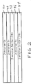
- Each misfit dislocation region consists of two 2 micron thick layers of silicon with 3% germanium, separated by a 2 micron layer of silicon with no germanium (see fig.2). Two layers of two microns thick silicon sub layers are deposited on top of the second SiGe layer.
- the epitaxial layer is grown. After the device if finished the epitaxial layer will include an N++ out diffusion buffer region 14. A P+ diffused region 18 is diffused into this epitaxial layer to create a P-N junction 20. If this P-N junction is reverse biased, a depletion region 16 will sustain the bias voltage.
- Depletion region 16 will contain N-type silicon with regions 22, 24 and 26 separated by regions 28, 30 and 32 containing misfit dislocations.
- Each of the misfit dislocation regions 28, 30 and 32 are preferably formed of five layers each approximately 2 microns thick.
- a typical region 28, 30 and 32 including misfit dislocations is illustrated in Figure 2.
- a first germanium containing layer 34 Si/Ge
- Si/Ge silicon/Ge
- a 4 min. hydrogen purge is performed to clean the gas in the chamber.
- a first substantially germanium free silicon layer 36 is then grown over layer 34.
- Layer 36 is also approximately 2 microns thick.
- a second germanium containing layer 38 is grown (Si/Ge) which is similar to layer 34 in composition and thickness. After this another purge. During this purge the temperature is raised to 1100°C. Above layer 38 another substantially germanium free layer 40 is grown. Then another purge and another substantially germanium free layer 42. Silicon sublayers 40 and 42, each are approximately two microns thick. Finally a gas etch etches away a part of layer 42 and another 4 min. hydrogen purge removes the etching gasses.
- Each multi-layer region of misfit dislocations has a thickness of approximately 10 microns.
- the regions are spaced apart by N-silicon regions 24 and 26 of approximately 13 microns thickness.
- Adjacent the surface of region 32 of misfit dislocations is grown an approximately 45 micron thick silicon buffer. A portion of the buffer will be diffused with a P type impurity to form a P+ type region 18 with a P/N junction 20.
- the regions of misfit dislocations are preferably proximate to junction 20.
- Fig. 3 shows the case where the misfit dislocation regions 28 and 30 are situated just outside the depletion region 16.
- the misfit dislocation regions are the same as earlier described and shown in Fig.2, however preferably with one two or more Ge doped layers.
- misfit dislocations as well as metal diffusion are employed to enhance the switching speed in devices such as power rectifiers.
- the misfit dislocations serve as getter sites of the metallic impurities.
- the metallic impurities are diffused all through the silicon and end up into the misfit dislocation regions as the regions are formed and remain in those regions in relatively large concentrations, as compared to the surface and remainder of the depletion region.
- the source of these metallic impurities can be a gold doped wafer in the vapor deposition reactor chamber.
- misfit dislocations are associated with deep energy levels in the energy gap of silicon. Misfit dislocations act as localized lifetime killers. The employment of such misfit dislocations is a controllable, clean technique for increasing switching speed of power rectifiers and reducing the minority carrier lifetime of mutilayer devices.
- misfit dislocations are effective gettering sites for metallic impurities. Small amounts of gold and platinum can easily be incorporated into the region of misfit dislocations, leaving the remaining silicon layers with minimal metallic impurity precipitates.
Applications Claiming Priority (2)
| Application Number | Priority Date | Filing Date | Title |
|---|---|---|---|
| US82951 | 1993-07-01 | ||
| US08/082,951 US5342805A (en) | 1993-07-01 | 1993-07-01 | Method of growing a semiconductor material by epilaxy |
Publications (3)
| Publication Number | Publication Date |
|---|---|
| EP0632486A2 true EP0632486A2 (de) | 1995-01-04 |
| EP0632486A3 EP0632486A3 (de) | 1995-03-29 |
| EP0632486B1 EP0632486B1 (de) | 2000-09-06 |
Family
ID=22174496
Family Applications (1)
| Application Number | Title | Priority Date | Filing Date |
|---|---|---|---|
| EP94302800A Expired - Lifetime EP0632486B1 (de) | 1993-07-01 | 1994-04-20 | Verfahren zur Herstellung epitaktischen Halbleitermaterials |
Country Status (7)
| Country | Link |
|---|---|
| US (1) | US5342805A (de) |
| EP (1) | EP0632486B1 (de) |
| JP (1) | JP2638737B2 (de) |
| KR (1) | KR0166989B1 (de) |
| DE (1) | DE69425787T2 (de) |
| SG (1) | SG47620A1 (de) |
| TW (1) | TW228608B (de) |
Families Citing this family (9)
| Publication number | Priority date | Publication date | Assignee | Title |
|---|---|---|---|---|
| US5640043A (en) * | 1995-12-20 | 1997-06-17 | General Instrument Corporation Of Delaware | High voltage silicon diode with optimum placement of silicon-germanium layers |
| DE69941446D1 (de) | 1998-04-09 | 2009-11-05 | Nxp Bv | Halbleiter mit gleichrichtendem übergang und seine herstellung |
| US6858503B1 (en) * | 2003-02-05 | 2005-02-22 | Advanced Micro Devices, Inc. | Depletion to avoid cross contamination |
| JP5067381B2 (ja) * | 2009-02-19 | 2012-11-07 | 東京エレクトロン株式会社 | 熱処理装置の運転方法 |
| JP2015149346A (ja) * | 2014-02-05 | 2015-08-20 | 三菱電機株式会社 | 半導体装置の製造方法および半導体装置 |
| WO2015128254A1 (en) | 2014-02-25 | 2015-09-03 | Koninklijke Philips N.V. | Light emitting semiconductor devices with getter layer |
| CN105814694B (zh) * | 2014-10-03 | 2019-03-08 | 富士电机株式会社 | 半导体装置以及半导体装置的制造方法 |
| JP7313201B2 (ja) * | 2019-06-14 | 2023-07-24 | 東京エレクトロン株式会社 | エッチング方法およびエッチング装置 |
| EP4576168A1 (de) * | 2023-12-22 | 2025-06-25 | Nexperia B.V. | Unterdrückung der selbstdotierung während des epitaktischen wachstums einer epitaxie-schicht in einer halbleitervorrichtung |
Family Cites Families (5)
| Publication number | Priority date | Publication date | Assignee | Title |
|---|---|---|---|---|
| US5084411A (en) * | 1988-11-29 | 1992-01-28 | Hewlett-Packard Company | Semiconductor processing with silicon cap over Si1-x Gex Film |
| JPH02235327A (ja) * | 1989-03-08 | 1990-09-18 | Fujitsu Ltd | 半導体成長装置および半導体成長方法 |
| US5097308A (en) * | 1990-03-13 | 1992-03-17 | General Instrument Corp. | Method for controlling the switching speed of bipolar power devices |
| US5102810A (en) * | 1990-03-13 | 1992-04-07 | General Instrument Corp. | Method for controlling the switching speed of bipolar power devices |
| DE4119531A1 (de) * | 1991-06-13 | 1992-12-17 | Wacker Chemitronic | Epitaxierte halbleiterscheiben mit sauerstoffarmer zone einstellbarer ausdehnung und verfahren zu ihrer herstellung |
-
1993
- 1993-07-01 US US08/082,951 patent/US5342805A/en not_active Expired - Lifetime
- 1993-07-13 TW TW082105580A patent/TW228608B/zh active
- 1993-09-13 JP JP5227114A patent/JP2638737B2/ja not_active Expired - Lifetime
-
1994
- 1994-04-14 KR KR1019940007815A patent/KR0166989B1/ko not_active Expired - Fee Related
- 1994-04-20 DE DE69425787T patent/DE69425787T2/de not_active Expired - Fee Related
- 1994-04-20 SG SG1996003229A patent/SG47620A1/en unknown
- 1994-04-20 EP EP94302800A patent/EP0632486B1/de not_active Expired - Lifetime
Also Published As
| Publication number | Publication date |
|---|---|
| US5342805A (en) | 1994-08-30 |
| HK1011793A1 (en) | 1999-07-16 |
| KR950004579A (ko) | 1995-02-18 |
| EP0632486B1 (de) | 2000-09-06 |
| JP2638737B2 (ja) | 1997-08-06 |
| KR0166989B1 (ko) | 1999-01-15 |
| DE69425787T2 (de) | 2001-01-04 |
| EP0632486A3 (de) | 1995-03-29 |
| TW228608B (en) | 1994-08-21 |
| JPH0737815A (ja) | 1995-02-07 |
| DE69425787D1 (de) | 2000-10-12 |
| SG47620A1 (en) | 1998-04-17 |
Similar Documents
| Publication | Publication Date | Title |
|---|---|---|
| US5413679A (en) | Method of producing a silicon membrane using a silicon alloy etch stop layer | |
| US4717681A (en) | Method of making a heterojunction bipolar transistor with SIPOS | |
| US6096627A (en) | Method for introduction of an impurity dopant in SiC, a semiconductor device formed by the method and a use of a highly doped amorphous layer as a source for dopant diffusion into SiC | |
| US4349394A (en) | Method of making a zener diode utilizing gas-phase epitaxial deposition | |
| US4466173A (en) | Methods for fabricating vertical channel buried grid field controlled devices including field effect transistors and field controlled thyristors utilizing etch and refill techniques | |
| US6114223A (en) | Gettering regions and methods of forming gettering regions within a semiconductor wafer | |
| US6339011B1 (en) | Method of forming semiconductive active area having a proximity gettering region therein and method of processing a monocrystalline silicon substrate to have a proximity gettering region | |
| US6909119B2 (en) | Low temperature formation of backside ohmic contacts for vertical devices | |
| EP0632486B1 (de) | Verfahren zur Herstellung epitaktischen Halbleitermaterials | |
| US4429324A (en) | Zener diode and method of making the same | |
| US5565690A (en) | Method for doping strained heterojunction semiconductor devices and structure | |
| EP0180457B1 (de) | Halbleiteranordnung mit einer integrierten Schaltung und Verfahren zu deren Herstellung | |
| EP0633606A1 (de) | Verfahren zur Herstellung einer Leistungsdiode | |
| US5352628A (en) | Method of forming diffusion region of semiconductor device by solid phase diffusion | |
| JP2755185B2 (ja) | Soi基板 | |
| US5141887A (en) | Low voltage, deep junction device and method | |
| EP0200059B1 (de) | Verfahren zur Herstellung eines ohmischen Kontaktes auf einem III-V Halbleiter und hergestelltes Halbleiterzwischenprodukt | |
| US5102810A (en) | Method for controlling the switching speed of bipolar power devices | |
| US5097308A (en) | Method for controlling the switching speed of bipolar power devices | |
| EP0935816B1 (de) | Verfahren zur herstellung einer halbleiteranordnung mit schottky-übergang | |
| JP3579069B2 (ja) | 半導体装置の製造方法 | |
| EP1008187B1 (de) | Halbleiter mit gleichrichtendem übergang und seine herstellung | |
| HK1011793B (en) | Method of fabricating epitaxial semiconductor material | |
| US20030222272A1 (en) | Semiconductor devices using minority carrier controlling substances | |
| EP0144545A2 (de) | Diffusionsverfahren zum Herstellen eines Thyristors |
Legal Events
| Date | Code | Title | Description |
|---|---|---|---|
| PUAI | Public reference made under article 153(3) epc to a published international application that has entered the european phase |
Free format text: ORIGINAL CODE: 0009012 |
|
| AK | Designated contracting states |
Kind code of ref document: A2 Designated state(s): DE FR GB IT NL |
|
| PUAL | Search report despatched |
Free format text: ORIGINAL CODE: 0009013 |
|
| AK | Designated contracting states |
Kind code of ref document: A3 Designated state(s): DE FR GB IT NL |
|
| 17P | Request for examination filed |
Effective date: 19950411 |
|
| 17Q | First examination report despatched |
Effective date: 19961004 |
|
| RAP1 | Party data changed (applicant data changed or rights of an application transferred) |
Owner name: GENERAL SEMICONDUCTOR, INC. |
|
| GRAG | Despatch of communication of intention to grant |
Free format text: ORIGINAL CODE: EPIDOS AGRA |
|
| RTI1 | Title (correction) |
Free format text: METHOD OF FABRICATING EPITAXIAL SEMICONDUCTOR MATERIAL |
|
| GRAG | Despatch of communication of intention to grant |
Free format text: ORIGINAL CODE: EPIDOS AGRA |
|
| GRAG | Despatch of communication of intention to grant |
Free format text: ORIGINAL CODE: EPIDOS AGRA |
|
| GRAH | Despatch of communication of intention to grant a patent |
Free format text: ORIGINAL CODE: EPIDOS IGRA |
|
| GRAH | Despatch of communication of intention to grant a patent |
Free format text: ORIGINAL CODE: EPIDOS IGRA |
|
| GRAA | (expected) grant |
Free format text: ORIGINAL CODE: 0009210 |
|
| AK | Designated contracting states |
Kind code of ref document: B1 Designated state(s): DE FR GB IT NL |
|
| ITF | It: translation for a ep patent filed | ||
| ET | Fr: translation filed | ||
| REF | Corresponds to: |
Ref document number: 69425787 Country of ref document: DE Date of ref document: 20001012 |
|
| PGFP | Annual fee paid to national office [announced via postgrant information from national office to epo] |
Ref country code: DE Payment date: 20010402 Year of fee payment: 8 |
|
| PG25 | Lapsed in a contracting state [announced via postgrant information from national office to epo] |
Ref country code: GB Free format text: LAPSE BECAUSE OF NON-PAYMENT OF DUE FEES Effective date: 20010420 |
|
| PLBE | No opposition filed within time limit |
Free format text: ORIGINAL CODE: 0009261 |
|
| STAA | Information on the status of an ep patent application or granted ep patent |
Free format text: STATUS: NO OPPOSITION FILED WITHIN TIME LIMIT |
|
| 26N | No opposition filed | ||
| GBPC | Gb: european patent ceased through non-payment of renewal fee |
Effective date: 20010420 |
|
| PG25 | Lapsed in a contracting state [announced via postgrant information from national office to epo] |
Ref country code: DE Free format text: LAPSE BECAUSE OF NON-PAYMENT OF DUE FEES Effective date: 20021101 |
|
| PGFP | Annual fee paid to national office [announced via postgrant information from national office to epo] |
Ref country code: NL Payment date: 20030403 Year of fee payment: 10 |
|
| PGFP | Annual fee paid to national office [announced via postgrant information from national office to epo] |
Ref country code: FR Payment date: 20030418 Year of fee payment: 10 |
|
| PG25 | Lapsed in a contracting state [announced via postgrant information from national office to epo] |
Ref country code: NL Free format text: LAPSE BECAUSE OF NON-PAYMENT OF DUE FEES Effective date: 20041101 |
|
| PG25 | Lapsed in a contracting state [announced via postgrant information from national office to epo] |
Ref country code: FR Free format text: LAPSE BECAUSE OF NON-PAYMENT OF DUE FEES Effective date: 20041231 |
|
| NLV4 | Nl: lapsed or anulled due to non-payment of the annual fee |
Effective date: 20041101 |
|
| REG | Reference to a national code |
Ref country code: FR Ref legal event code: ST |
|
| PG25 | Lapsed in a contracting state [announced via postgrant information from national office to epo] |
Ref country code: IT Free format text: LAPSE BECAUSE OF NON-PAYMENT OF DUE FEES Effective date: 20050420 |