EP0632501A1 - Dispositif semi-conducteur comprenant des moyens de protection - Google Patents
Dispositif semi-conducteur comprenant des moyens de protection Download PDFInfo
- Publication number
- EP0632501A1 EP0632501A1 EP94201869A EP94201869A EP0632501A1 EP 0632501 A1 EP0632501 A1 EP 0632501A1 EP 94201869 A EP94201869 A EP 94201869A EP 94201869 A EP94201869 A EP 94201869A EP 0632501 A1 EP0632501 A1 EP 0632501A1
- Authority
- EP
- European Patent Office
- Prior art keywords
- region
- insulated gate
- semiconductor device
- parasitic bipolar
- coupled
- Prior art date
- Legal status (The legal status is an assumption and is not a legal conclusion. Google has not performed a legal analysis and makes no representation as to the accuracy of the status listed.)
- Granted
Links
Images



Classifications
-
- H—ELECTRICITY
- H10—SEMICONDUCTOR DEVICES; ELECTRIC SOLID-STATE DEVICES NOT OTHERWISE PROVIDED FOR
- H10D—INORGANIC ELECTRIC SEMICONDUCTOR DEVICES
- H10D30/00—Field-effect transistors [FET]
- H10D30/60—Insulated-gate field-effect transistors [IGFET]
- H10D30/64—Double-diffused metal-oxide semiconductor [DMOS] FETs
- H10D30/66—Vertical DMOS [VDMOS] FETs
-
- H—ELECTRICITY
- H10—SEMICONDUCTOR DEVICES; ELECTRIC SOLID-STATE DEVICES NOT OTHERWISE PROVIDED FOR
- H10D—INORGANIC ELECTRIC SEMICONDUCTOR DEVICES
- H10D1/00—Resistors, capacitors or inductors
- H10D1/40—Resistors
- H10D1/43—Resistors having PN junctions
-
- H—ELECTRICITY
- H10—SEMICONDUCTOR DEVICES; ELECTRIC SOLID-STATE DEVICES NOT OTHERWISE PROVIDED FOR
- H10D—INORGANIC ELECTRIC SEMICONDUCTOR DEVICES
- H10D30/00—Field-effect transistors [FET]
- H10D30/60—Insulated-gate field-effect transistors [IGFET]
-
- H—ELECTRICITY
- H10—SEMICONDUCTOR DEVICES; ELECTRIC SOLID-STATE DEVICES NOT OTHERWISE PROVIDED FOR
- H10D—INORGANIC ELECTRIC SEMICONDUCTOR DEVICES
- H10D64/00—Electrodes of devices having potential barriers
- H10D64/20—Electrodes characterised by their shapes, relative sizes or dispositions
- H10D64/23—Electrodes carrying the current to be rectified, amplified, oscillated or switched, e.g. sources, drains, anodes or cathodes
- H10D64/251—Source or drain electrodes for field-effect devices
- H10D64/256—Source or drain electrodes for field-effect devices for lateral devices wherein the source or drain electrodes are recessed in semiconductor bodies
-
- H—ELECTRICITY
- H10—SEMICONDUCTOR DEVICES; ELECTRIC SOLID-STATE DEVICES NOT OTHERWISE PROVIDED FOR
- H10D—INORGANIC ELECTRIC SEMICONDUCTOR DEVICES
- H10D8/00—Diodes
-
- H—ELECTRICITY
- H10—SEMICONDUCTOR DEVICES; ELECTRIC SOLID-STATE DEVICES NOT OTHERWISE PROVIDED FOR
- H10D—INORGANIC ELECTRIC SEMICONDUCTOR DEVICES
- H10D8/00—Diodes
- H10D8/20—Breakdown diodes, e.g. avalanche diodes
- H10D8/25—Zener diodes
-
- H—ELECTRICITY
- H10—SEMICONDUCTOR DEVICES; ELECTRIC SOLID-STATE DEVICES NOT OTHERWISE PROVIDED FOR
- H10D—INORGANIC ELECTRIC SEMICONDUCTOR DEVICES
- H10D84/00—Integrated devices formed in or on semiconductor substrates that comprise only semiconducting layers, e.g. on Si wafers or on GaAs-on-Si wafers
- H10D84/101—Integrated devices comprising main components and built-in components, e.g. IGBT having built-in freewheel diode
- H10D84/141—VDMOS having built-in components
-
- H—ELECTRICITY
- H10—SEMICONDUCTOR DEVICES; ELECTRIC SOLID-STATE DEVICES NOT OTHERWISE PROVIDED FOR
- H10D—INORGANIC ELECTRIC SEMICONDUCTOR DEVICES
- H10D84/00—Integrated devices formed in or on semiconductor substrates that comprise only semiconducting layers, e.g. on Si wafers or on GaAs-on-Si wafers
- H10D84/101—Integrated devices comprising main components and built-in components, e.g. IGBT having built-in freewheel diode
- H10D84/141—VDMOS having built-in components
- H10D84/148—VDMOS having built-in components the built-in components being breakdown diodes, e.g. Zener diodes
-
- H—ELECTRICITY
- H10—SEMICONDUCTOR DEVICES; ELECTRIC SOLID-STATE DEVICES NOT OTHERWISE PROVIDED FOR
- H10D—INORGANIC ELECTRIC SEMICONDUCTOR DEVICES
- H10D89/00—Aspects of integrated devices not covered by groups H10D84/00 - H10D88/00
- H10D89/60—Integrated devices comprising arrangements for electrical or thermal protection, e.g. protection circuits against electrostatic discharge [ESD]
- H10D89/601—Integrated devices comprising arrangements for electrical or thermal protection, e.g. protection circuits against electrostatic discharge [ESD] for devices having insulated gate electrodes, e.g. for IGFETs or IGBTs
Definitions
- This invention relates to a semiconductor device, in particular a semiconductor device comprising an insulated gate field effect transistor integrated within the same semiconductor body as one or more further components for controlling or protecting the insulated gate field effect transistor.
- the insulated gate field effect transistor may be a vertical power MOSFET of the so-called DMOS type where the term "vertical" means that the main current in normal operation of the MOSFET is between opposed first and second major surfaces
- DMOS vertical power MOSFET
- protected switches or smart power devices have been proposed in which one or more additional components for controlling or protecting the insulated gate field effect transistor are integrated within the same semiconductor body as the insulated gate field effect transistor.
- US-A-4760434 describes a vertical type MOSFET with on chip thermal and other protection in which some of the additional components are formed as thin film devices provided on top of and isolated from insulated gate field effect transistor or MOSFET and some integrated within an opposite conductivity type isolation well region provided within a first region which generally is an epitaxial layer and forms at least a drain drift region of the semiconductor body.
- a first region which generally is an epitaxial layer and forms at least a drain drift region of the semiconductor body.
- a semiconductor device comprising a semiconductor body having first and second major surfaces with a first region of one conductivity type adjacent the first major surface, an insulated gate field effect transistor formed within the first region and having source and drain electrodes and an insulated gate electrode, at least one further component coupled between the insulated gate electrode of the insulated gate field effect transistor and a gate input terminal, the further component requiring a second region of the opposite conductivity type provided within the first region so that a region of the further component, the second region and the first region form a parasitic bipolar transistor and, provided on an insulating layer on the first major surface, a first rectifying element coupled between the base region of the parasitic bipolar transistor and the gate input terminal and a second rectifying element coupled between the emitter region of the parasitic bipolar transistor and the gate input terminal for causing, when the voltage between the source and insulated gate electrodes reverses sign, the first and second rectifying elements in series with the base and emitter regions of the parasitic bipolar transistor to become forward-biassed to reduce the
- the first and second rectifying elements act to reduce the base-emitter voltage of the parasitic bipolar transistor and so reduce the possibility of unwanted bipolar action.
- a third rectifying element may be coupled in anti-parallel with the second rectifying element to facilitate the supply of gate drive to the insulated gate field effect transistor under normal operating conditions.
- a fourth rectifying element may be coupled in series with the second rectifying element to further reduce the base-emitter voltage which can be applied across the parasitic bipolar transistor.
- the rectifying elements may comprise thin film diodes, for example polycrystalline silicon diodes.
- the insulated gate field effect transistor may comprise a vertical insulated gate field effect transistor with the source electrode at the first major surface and the drain electrode at the second major surface.
- the insulated gate field effect transistor may comprise a plurality of second regions of the opposite conductivity type formed within the first region adjacent the first major surface and each containing a source region of the one conductivity type coupled to the source electrode, with the insulated gate electrode overlying a conduction channel area of each second region to define a gateable conductive path between the source regions and the first region which forms at least part of a drain region coupled to the drain electrode of the insulated gate field effect transistor.
- the second region may form a well or isolation region within which the at least one further component is formed.
- the at least one further component may comprise an insulated gate field effect transistor of the one conductivity type or a diffused resistor of the one conductivity type formed within the well region.
- the at least one further component could be an electrostatic protection diode with the second region forming one of the regions of the diode. Also, any two or more of these different types of components may be provided in the semiconductor body.
- the first and second rectifying elements D1 and D2 act to reduce the base-emitter voltage of the parasitic bipolar transistor B and so reduce the possibility of unwanted bipolar action.
- FIG. 1 there is illustrated a very simplified circuit diagram of a known protected switch 1' marketed by Philips Semiconductors as a TOPFET (Trade Mark) protected switch.
- the protected switch 1' comprises an n-channel enhancement mode power MOSFET 6 of the vertical DMOS type.
- the MOSFET 6 is intended to be connected as a low-side switch to a suitable load L such as an automotive light or motor coil or similar. Accordingly, the drain electrode D of the MOSFET 1' is coupled to a terminal T to which one terminal or end of the load L is to be connected while the source electrode S is coupled to a power supply line 10 which in use is coupled to a reference potential, generally ground, and the other terminal of the load L is coupled to a positive voltage supply line 11.
- the insulated gate electrode G of the MOSFET 6 is coupled to the gate terminal GT to which an appropriate gate drive circuit will be coupled in use via gate input resistors, three of which R3, R4 and R5 are shown in Figure 1.
- a voltage clamping circuit 13 is coupled between the drain and gate electrodes D and G of the MOSFET 1 to protect the MOSFET during switching of an inductive load, in particular to turn the MOSFET back on in the event of an inductive load causing an over-voltage at the drain electrode D.
- Any suitable form of voltage clamping circuit may be used.
- a circuit such as that described in our EP-A-523800 may be used.
- One or more protection zener diodes may be provided at the gate input. Two zener diodes ZD1 and ZD2 are shown.
- the protected switch shown in Figure 1 also includes a further protection circuit 14 which is coupled to the gate of an N-channel enhancement mode IGFET 15 having its main source-to-drain current path coupled between the gate G and source S electrodes (as shown to the supply line 10) to cause the gate to be pulled low, connected to ground in this case, in the event of an undesired condition being detected.
- the undesired condition may be, for example, a short-circuit or over-temperature and the further protection circuit 14 may have any suitable form.
- an over-temperature detection circuit such as described in EP-A-360333, EP-A-369530 or EP-A-479362 may be used in appropriate circumstances.
- the parasitic bipolar transistor B which is inherent in the protected switch is shown in phantom lines in Figure 1.
- Figure 2 illustrates by way of cross-sectional views of different parts of a semiconductor body 2 how different components which may be used in a protected switch such as that shown in Figure 1 may be formed.
- the semiconductor body 2 comprises, in this example, a relatively highly doped n conductivity single crystal silicon substrate 2a on which is provided a relatively lowly doped n conductivity type silicon epitaxial layer 2b which forms the first region, generally the drain drift region, of the MOSFET 6.
- the MOSFET 6 is formed using conventional DMOS processing technology and one cell 6a of the MOSFET 6 is shown in Figure 2a.
- the cell 6a comprises adjacent one major surface 2c of the semiconductor body 2 a p conductivity body region 16 which contains an n conductivity source region 17 and defines therewith a conduction channel area 16b under the insulated gate 18 of the MOSFET.
- the p body region 16 may have a central relatively highly doped subsidiary region 16a which is shorted (either as shown by a moat etched through the source region 17 or by masking the source implant) to the source electrode S to inhibit parasitic bipolar action.
- the source electrode S and gate electrode G are formed by metallisation provided on top of an insulating layer 30 and making contact to the source regions 17 and insulated gate 18, respectively, via appropriate contact holes.
- the drain electrode D is provided on the other major surface 2d of the semiconductor body 2.
- Figure 2b shows a lateral NMOS transistor, for example the transistor 15 shown in Figure 1, having source and drain regions 19 and 20 diffused in a p conductivity second region which in this example forms an isolation or well region 21 and an overlying insulated gate 22 and source, gate and drain electrodes 23, 24 and 25 formed on the insulating layer 30.
- a parasitic bipolar transistor exists between the source region 19, the well region 21 and the first region 2b.
- Figure 2c shows a diffused resistor, for example the resistor R4, which consists of an n conductivity region 26 within a p conductivity well or isolation region which may be the same region 21.
- An electrode 27 couples the well region 21 to a reference potential which is generally ground and resistor electrodes 28a and 28b are provided at each end of the region 26.
- a parasitic bipolar transistor exists between the region 26, the well region 21 and the first region 2b.
- Figure 2d shows a diffused diode, for example the zener diode ZD1, consisting of a relatively highly doped p conductivity region 29 within which is provided an n conductivity region 31 together with appropriate electrodes 29a and 31a making contact through contact holes in the insulating layer 30.
- a parasitic bipolar transistor exists between the first region 2b and the regions 29 and 31 of the diode ZD1.
- Figure 2e shows a thin film diode D1 while Figure 2f shows a thin film resistor, for example R3, formed on top of the insulating layer 30, usually over the well region 21.
- the diode D1 is a pn junction diode consisting of oppositely doped regions 32 and 33 of polycrystalline silicon with respective electrodes 32a and 33a making contact through openings in an insulating layer 34 while the resistor R3 is generally formed by an n conductivity doped polycrystalline silicon region 35 with respective electrodes 35a and 35b making contact through openings in the insulating layer 34.
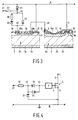
- Figure 3 illustrates by way of a part-cross-sectional and part circuit diagrammatic drawing, a first example of a semiconductor device 1a in accordance with the invention.
- a semiconductor device 1a in accordance with the invention.
- only one cell 6a of the MOSFET 6 is shown and one further component coupled to the insulated gate G of the MOSFET by a line 40 and to the gate input terminal GT via diodes D1, D2 and D3 (as will be described below) is shown.
- the further component is shown as a diffused resistor R4, but could be a diffused lateral N channel MOSFET or a diffused diode as shown in Figure 2.
- the electrode 27 is coupled to the source electrode S, that is to the ground power supply line 10 while the resistor electrode 28a is coupled via a node 42 to the anode of the thin film diode D2 and to the cathode of the thin film diode D3.
- the other electrodes of the two diodes D2 and D3 are coupled via a node 41 to the cathode of a thin film diode D1 having its anode coupled to the source electrode S or supply line 10.
- An optional thin film resistor R6 may be provided between diode D2 and the node 41.
- FIG. 3 is a simplified circuit diagram showing the general circuit where the box labeled P represents the logic components such as the resistor shown in Figure 3.
- This circuit should protect the MOSFET 6 from damage when the voltage at the gate input goes negative with respect to the source voltage of the MOSFET 6.
- the voltage at node 41 will be, typically, 0.5 volts above the input voltage (that is the voltage at node 42) and as the MOSFET is turned off, the input voltage will fall quickly to 0.5 volts and more slowly to zero volts as determined by the internal input-source resistance which may typically be 65 kilo-ohms.
- the MOSFET 6 When the input voltage is 0.5 volts, the MOSFET 6 will be below threshold and so no current will pass through the load.
- Figure 5 is a circuit diagram for illustrating the effect of the parasitic bipolar transistor B formed by the one or more further components.
- the first region 2b forms the collector region (and is coupled to the drain electrode D) of the parasitic bipolar transistor B
- the well region 21 forms the base region (and is coupled via the diode D1 to node 41 and to the gate input terminal GT)
- an n conductivity region region 26 in this example forms the emitter region and is coupled to the node 42.
- the diode D2 reduces the base-emitter voltage Vbe of the parasitic bipolar transistor B to a proportion (dependent on the diodes D1 and D2) of the forward voltage Vf of the diode D1.
- diodes D1 and D2 are similar and so the proportion is a half. This limits the base current of the bipolar transistor B to a negligible value so that the full BVces (collector-emitter saturated voltage) can be achieved.
- the diode D1 also acts to reduce the thermal leakage base current of the parasitic bipolar transistor B .
- the diode D3 acts to facilitate normal operation of the MOSFET 6.
- the resistor R6 may optionally be provided if a negative voltage is likely to arise at the input for considerably longer than two milliseconds. This resistor R6 should be sufficiently large to keep the current flowing through the input small during a negative input voltage situation.
- FIGs 6 and 7 illustrate an alternative in which a further thin film diode D4 is provided in series with the diode D2. Assuming the diodes are similar then this arrangement will reduce the Vbe of the parasitic transistor B to one third (as opposed to a half in Figures 4 and 5) of the Vf of the diode D1 and will also comparatively reduce the turn off time of the MOSFET 6. Of course, further diodes could be added to further reduce the Vbe of the parasitic transistor B.
- a semiconductor device in accordance with the invention should thus avoid or at least reduce the possibility of parasitic bipolar action due to further components such as those mentioned above integrated in the semiconductor body 2, may also remove the need for integral ESD protection diodes and certainly should assist in avoiding the situation where parasitic bipolar action arises because the parasitic bipolar transistor which is part of the ESD protection diode has a BVceo lower than the voltage at which the clamping circuit 13 operates.
- a negative input voltage can be created by a combination of high current in the MOSFET 6, significant wiring resistance between the source electrode and ground or if separate grounds are used for the MOSFET and the gate driving circuit.
- the clamping circuit may become operational and a voltage may be generated in the source-ground wiring which, in the absence of the present invention, would provide a voltage greater than the Vbe of the parasitic bipolar transistor B. The present invention thus prevents or at least inhibits failure of the MOSFET under such circumstances.
- the present invention may be applied to a high-side switch, that is where the MOSFET 6 is connected between the positive power supply line 11 and the load L to inhibit the turn on of parasitic bipolar transistors which might otherwise arise if a supply line 11 over-voltage transient results in the clamping circuit 13 operating causing the MOSFET to conduct and potentially raising the potential of the source above ground so that, if the gate is held at ground, the gate becomes negative with respect to the source.
- the present invention could be applied to P channel devices with appropriate modification and it should be understood that a reference to the voltage difference between the source and gate reversing sign means the situation when this voltage difference is of the opposite sign to that required for the MOSFET 6 to be conducting.
- the diode D1, D2 and D3 arrangement could be provided for one or more of any further components integrated with the MOSFET, depending upon the likelihood of a particular component causing parasitic bipolar action.
- the present invention could of course be applied to semiconductor materials other than silicon.
Landscapes
- Metal-Oxide And Bipolar Metal-Oxide Semiconductor Integrated Circuits (AREA)
- Semiconductor Integrated Circuits (AREA)
- Insulated Gate Type Field-Effect Transistor (AREA)
Applications Claiming Priority (2)
| Application Number | Priority Date | Filing Date | Title |
|---|---|---|---|
| GB939313651A GB9313651D0 (en) | 1993-07-01 | 1993-07-01 | A semiconductor device |
| GB9313651 | 1993-07-01 |
Publications (2)
| Publication Number | Publication Date |
|---|---|
| EP0632501A1 true EP0632501A1 (fr) | 1995-01-04 |
| EP0632501B1 EP0632501B1 (fr) | 1999-11-24 |
Family
ID=10738147
Family Applications (1)
| Application Number | Title | Priority Date | Filing Date |
|---|---|---|---|
| EP94201869A Expired - Lifetime EP0632501B1 (fr) | 1993-07-01 | 1994-06-29 | Dispositif semi-conducteur comprenant des moyens de protection |
Country Status (5)
| Country | Link |
|---|---|
| US (1) | US5466952A (fr) |
| EP (1) | EP0632501B1 (fr) |
| JP (1) | JP3665367B2 (fr) |
| DE (1) | DE69421758T2 (fr) |
| GB (1) | GB9313651D0 (fr) |
Cited By (4)
| Publication number | Priority date | Publication date | Assignee | Title |
|---|---|---|---|---|
| WO1997030481A1 (fr) * | 1996-02-19 | 1997-08-21 | Siemens Aktiengesellschaft | Circuit integre pour la commande d'un transistor de puissance a effet de champ mos avec charge cote source |
| EP0808024A3 (fr) * | 1996-05-17 | 2000-01-12 | Delco Electronics Corporation | Dispositif électrique d'attaque de charge comprenant un circuit de limitation de courant de charge |
| EP0809295A3 (fr) * | 1996-05-21 | 2000-07-05 | Siemens Aktiengesellschaft | Mosfet avec protection en température |
| EP1063757A3 (fr) * | 1999-05-05 | 2001-12-05 | SILICONIX Incorporated | MOSFET de puissance avec grille prépolarisée |
Families Citing this family (6)
| Publication number | Priority date | Publication date | Assignee | Title |
|---|---|---|---|---|
| DE69432016T2 (de) * | 1994-09-13 | 2004-01-08 | Stmicroelectronics S.R.L., Agrate Brianza | Verfahren zur Herstellung integrierter Schaltungen und erzeugte Halbleiterscheibe |
| US5808947A (en) * | 1995-08-21 | 1998-09-15 | Sgs-Thomson Microelectronics, Inc. | Integrated circuit that supports and method for wafer-level testing |
| US5861660A (en) * | 1995-08-21 | 1999-01-19 | Stmicroelectronics, Inc. | Integrated-circuit die suitable for wafer-level testing and method for forming the same |
| JP3414645B2 (ja) * | 1998-06-26 | 2003-06-09 | 沖電気工業株式会社 | 半導体装置 |
| US6833590B2 (en) * | 2001-01-11 | 2004-12-21 | Renesas Technology Corp. | Semiconductor device |
| JP4052923B2 (ja) * | 2002-10-25 | 2008-02-27 | 株式会社ルネサステクノロジ | 半導体装置 |
Citations (3)
| Publication number | Priority date | Publication date | Assignee | Title |
|---|---|---|---|---|
| JPS59232452A (ja) * | 1983-06-16 | 1984-12-27 | Nec Corp | Cmos集積回路 |
| JPS6091675A (ja) * | 1983-10-25 | 1985-05-23 | Matsushita Electric Ind Co Ltd | 半導体装置 |
| US4760434A (en) * | 1985-11-29 | 1988-07-26 | Nippondenso Co., Ltd. | Semiconductor device with protective means against overheating |
Family Cites Families (5)
| Publication number | Priority date | Publication date | Assignee | Title |
|---|---|---|---|---|
| GB2222884A (en) * | 1988-09-19 | 1990-03-21 | Philips Electronic Associated | Temperature sensing circuit |
| GB2224846A (en) * | 1988-11-14 | 1990-05-16 | Philips Electronic Associated | Temperature sensing circuit |
| GB2248151A (en) * | 1990-09-24 | 1992-03-25 | Philips Electronic Associated | Temperature sensing and protection circuit. |
| EP0523800B1 (fr) * | 1991-07-19 | 1998-04-08 | Philips Electronics Uk Limited | Commutateur semi-conducteur protégé contre les surtensions |
| GB9216953D0 (en) * | 1992-08-11 | 1992-09-23 | Philips Electronics Uk Ltd | A semiconductor component |
-
1993
- 1993-07-01 GB GB939313651A patent/GB9313651D0/en active Pending
-
1994
- 1994-06-28 JP JP14638794A patent/JP3665367B2/ja not_active Expired - Fee Related
- 1994-06-29 EP EP94201869A patent/EP0632501B1/fr not_active Expired - Lifetime
- 1994-06-29 DE DE69421758T patent/DE69421758T2/de not_active Expired - Lifetime
- 1994-06-30 US US08/269,810 patent/US5466952A/en not_active Expired - Lifetime
Patent Citations (3)
| Publication number | Priority date | Publication date | Assignee | Title |
|---|---|---|---|---|
| JPS59232452A (ja) * | 1983-06-16 | 1984-12-27 | Nec Corp | Cmos集積回路 |
| JPS6091675A (ja) * | 1983-10-25 | 1985-05-23 | Matsushita Electric Ind Co Ltd | 半導体装置 |
| US4760434A (en) * | 1985-11-29 | 1988-07-26 | Nippondenso Co., Ltd. | Semiconductor device with protective means against overheating |
Non-Patent Citations (2)
| Title |
|---|
| PATENT ABSTRACTS OF JAPAN vol. 9, no. 106 (E - 313) 10 May 1985 (1985-05-10) * |
| PATENT ABSTRACTS OF JAPAN vol. 9, no. 240 (E - 345) 26 September 1985 (1985-09-26) * |
Cited By (5)
| Publication number | Priority date | Publication date | Assignee | Title |
|---|---|---|---|---|
| WO1997030481A1 (fr) * | 1996-02-19 | 1997-08-21 | Siemens Aktiengesellschaft | Circuit integre pour la commande d'un transistor de puissance a effet de champ mos avec charge cote source |
| US6054738A (en) * | 1996-02-19 | 2000-04-25 | Siemens Aktiengesellschaft | Integrated circuit configuration for driving a power MOSFET with a load on the source side |
| EP0808024A3 (fr) * | 1996-05-17 | 2000-01-12 | Delco Electronics Corporation | Dispositif électrique d'attaque de charge comprenant un circuit de limitation de courant de charge |
| EP0809295A3 (fr) * | 1996-05-21 | 2000-07-05 | Siemens Aktiengesellschaft | Mosfet avec protection en température |
| EP1063757A3 (fr) * | 1999-05-05 | 2001-12-05 | SILICONIX Incorporated | MOSFET de puissance avec grille prépolarisée |
Also Published As
| Publication number | Publication date |
|---|---|
| DE69421758T2 (de) | 2000-06-08 |
| JP3665367B2 (ja) | 2005-06-29 |
| GB9313651D0 (en) | 1993-08-18 |
| DE69421758D1 (de) | 1999-12-30 |
| JPH0758331A (ja) | 1995-03-03 |
| US5466952A (en) | 1995-11-14 |
| EP0632501B1 (fr) | 1999-11-24 |
Similar Documents
| Publication | Publication Date | Title |
|---|---|---|
| EP0505191B1 (fr) | Dispositif à semiconducteur avec une région n à basse concentration pour améliorer les propriétés dV/dt | |
| US5963407A (en) | Overvoltage protection device for the protection of a power transistor having a MOS control terminal | |
| US5126911A (en) | Integrated circuit self-protected against reversal of the supply battery polarity | |
| EP0733283B1 (fr) | Commutateur protege | |
| US5221850A (en) | Conductivity-modulating mosfet | |
| JPH02185069A (ja) | 高エネルギー阻止能力及び温度補償された阻止電圧を具備する半導体デバイス | |
| EP3987661B1 (fr) | Conception de dispositif pour la protection contre les courts-circuits de transistors | |
| EP0523800B1 (fr) | Commutateur semi-conducteur protégé contre les surtensions | |
| JP3164065B2 (ja) | 半導体装置 | |
| KR100388727B1 (ko) | 보호스위치및차량의전기시스템 | |
| CN101019319A (zh) | 半导体开关装置和电子设备 | |
| US6469352B2 (en) | Two-terminal semiconductor overcurrent limiter | |
| US5466952A (en) | Semiconductor device having an IGET and a control or protection component | |
| EP1137068B1 (fr) | Dispositif semi-conducteur de puissance ayant un circuit de protection | |
| US5401996A (en) | Overvoltage protected semiconductor switch | |
| US10944257B2 (en) | Integrated silicon controlled rectifier (SCR) and a low leakage SCR supply clamp for electrostatic discharge (ESP) protection | |
| JP2004356622A (ja) | 接合型電子部品および前記電子部品を含む集積された電力装置 | |
| KR100200538B1 (ko) | 부성 저항 특성을 갖는 보호소자를 구비한 반도체장치 | |
| JP3139223B2 (ja) | 半導体装置及びその製造方法 | |
| JP3559075B2 (ja) | Cmos技術の集積電子回路用の極性反転保護装置 | |
| US6518815B2 (en) | Power device with protection against undesirable self-activation | |
| US6201677B1 (en) | Insulated gate type semiconductor apparatus with a control circuit | |
| US4893212A (en) | Protection of power integrated circuits against load voltage surges | |
| JP2870558B2 (ja) | 自動車用パワー集積回路 | |
| JP3884849B2 (ja) | 制御回路内蔵絶縁ゲート型半導体装置 |
Legal Events
| Date | Code | Title | Description |
|---|---|---|---|
| PUAI | Public reference made under article 153(3) epc to a published international application that has entered the european phase |
Free format text: ORIGINAL CODE: 0009012 |
|
| AK | Designated contracting states |
Kind code of ref document: A1 Designated state(s): DE FR GB IT NL |
|
| 17P | Request for examination filed |
Effective date: 19950704 |
|
| 17Q | First examination report despatched |
Effective date: 19970228 |
|
| GRAG | Despatch of communication of intention to grant |
Free format text: ORIGINAL CODE: EPIDOS AGRA |
|
| GRAG | Despatch of communication of intention to grant |
Free format text: ORIGINAL CODE: EPIDOS AGRA |
|
| GRAH | Despatch of communication of intention to grant a patent |
Free format text: ORIGINAL CODE: EPIDOS IGRA |
|
| GRAH | Despatch of communication of intention to grant a patent |
Free format text: ORIGINAL CODE: EPIDOS IGRA |
|
| GRAA | (expected) grant |
Free format text: ORIGINAL CODE: 0009210 |
|
| AK | Designated contracting states |
Kind code of ref document: B1 Designated state(s): DE FR GB IT NL |
|
| PG25 | Lapsed in a contracting state [announced via postgrant information from national office to epo] |
Ref country code: NL Free format text: LAPSE BECAUSE OF FAILURE TO SUBMIT A TRANSLATION OF THE DESCRIPTION OR TO PAY THE FEE WITHIN THE PRESCRIBED TIME-LIMIT Effective date: 19991124 Ref country code: IT Free format text: LAPSE BECAUSE OF FAILURE TO SUBMIT A TRANSLATION OF THE DESCRIPTION OR TO PAY THE FEE WITHIN THE PRE;WARNING: LAPSES OF ITALIAN PATENTS WITH EFFECTIVE DATE BEFORE 2007 MAY HAVE OCCURRED AT ANY TIME BEFORE 2007. THE CORRECT EFFECTIVE DATE MAY BE DIFFERENT FROM THE ONE RECORDED.SCRIBED TIME-LIMIT Effective date: 19991124 |
|
| REF | Corresponds to: |
Ref document number: 69421758 Country of ref document: DE Date of ref document: 19991230 |
|
| ET | Fr: translation filed | ||
| NLV1 | Nl: lapsed or annulled due to failure to fulfill the requirements of art. 29p and 29m of the patents act | ||
| PLBE | No opposition filed within time limit |
Free format text: ORIGINAL CODE: 0009261 |
|
| STAA | Information on the status of an ep patent application or granted ep patent |
Free format text: STATUS: NO OPPOSITION FILED WITHIN TIME LIMIT |
|
| 26N | No opposition filed | ||
| REG | Reference to a national code |
Ref country code: GB Ref legal event code: IF02 |
|
| REG | Reference to a national code |
Ref country code: FR Ref legal event code: TP |
|
| REG | Reference to a national code |
Ref country code: GB Ref legal event code: 732E |
|
| PGFP | Annual fee paid to national office [announced via postgrant information from national office to epo] |
Ref country code: DE Payment date: 20120524 Year of fee payment: 19 |
|
| PGFP | Annual fee paid to national office [announced via postgrant information from national office to epo] |
Ref country code: GB Payment date: 20120525 Year of fee payment: 19 Ref country code: FR Payment date: 20120705 Year of fee payment: 19 |
|
| GBPC | Gb: european patent ceased through non-payment of renewal fee |
Effective date: 20130629 |
|
| REG | Reference to a national code |
Ref country code: DE Ref legal event code: R119 Ref document number: 69421758 Country of ref document: DE Effective date: 20140101 |
|
| REG | Reference to a national code |
Ref country code: FR Ref legal event code: ST Effective date: 20140228 |
|
| PG25 | Lapsed in a contracting state [announced via postgrant information from national office to epo] |
Ref country code: GB Free format text: LAPSE BECAUSE OF NON-PAYMENT OF DUE FEES Effective date: 20130629 Ref country code: DE Free format text: LAPSE BECAUSE OF NON-PAYMENT OF DUE FEES Effective date: 20140101 |
|
| PG25 | Lapsed in a contracting state [announced via postgrant information from national office to epo] |
Ref country code: FR Free format text: LAPSE BECAUSE OF NON-PAYMENT OF DUE FEES Effective date: 20130701 |