EP0632579A2 - Gleichstromsteuerungsschaltung in Burst-Datenempfängern - Google Patents
Gleichstromsteuerungsschaltung in Burst-Datenempfängern Download PDFInfo
- Publication number
- EP0632579A2 EP0632579A2 EP94107895A EP94107895A EP0632579A2 EP 0632579 A2 EP0632579 A2 EP 0632579A2 EP 94107895 A EP94107895 A EP 94107895A EP 94107895 A EP94107895 A EP 94107895A EP 0632579 A2 EP0632579 A2 EP 0632579A2
- Authority
- EP
- European Patent Office
- Prior art keywords
- signal
- amplifier
- circuit
- current
- control circuit
- Prior art date
- Legal status (The legal status is an assumption and is not a legal conclusion. Google has not performed a legal analysis and makes no representation as to the accuracy of the status listed.)
- Granted
Links
- 239000003990 capacitor Substances 0.000 claims abstract description 16
- 238000006243 chemical reaction Methods 0.000 claims description 3
- 125000004122 cyclic group Chemical group 0.000 claims description 2
- 238000000034 method Methods 0.000 claims 2
- 238000005259 measurement Methods 0.000 claims 1
- 238000005070 sampling Methods 0.000 claims 1
- 230000005540 biological transmission Effects 0.000 abstract description 5
- 239000013307 optical fiber Substances 0.000 abstract description 5
- 230000003287 optical effect Effects 0.000 description 4
- 230000032683 aging Effects 0.000 description 2
- 230000018109 developmental process Effects 0.000 description 2
- 235000001537 Ribes X gardonianum Nutrition 0.000 description 1
- 235000001535 Ribes X utile Nutrition 0.000 description 1
- 235000016919 Ribes petraeum Nutrition 0.000 description 1
- 244000281247 Ribes rubrum Species 0.000 description 1
- 235000002355 Ribes spicatum Nutrition 0.000 description 1
- 238000012512 characterization method Methods 0.000 description 1
- 230000008878 coupling Effects 0.000 description 1
- 238000010168 coupling process Methods 0.000 description 1
- 238000005859 coupling reaction Methods 0.000 description 1
- 238000001514 detection method Methods 0.000 description 1
- 230000000694 effects Effects 0.000 description 1
- 230000000737 periodic effect Effects 0.000 description 1
Images


Classifications
-
- H—ELECTRICITY
- H03—ELECTRONIC CIRCUITRY
- H03F—AMPLIFIERS
- H03F1/00—Details of amplifiers with only discharge tubes, only semiconductor devices or only unspecified devices as amplifying elements
- H03F1/30—Modifications of amplifiers to reduce influence of variations of temperature or supply voltage or other physical parameters
Definitions
- This invention concerns a circuit that restores the variations in DC level present in the signal received by a bursted data receiver, in such a way that the increases in this level resulting from the reception of the data bursts are eliminated.
- Optical receivers contain an opto-electrical transducer based generally on a PINFET and an amplifier that produces at its output an electrical signal with an amplitude proportional to the optical power received over an optical fibre.
- the received bursts have a major low frequency component, meaning that the time constant of the circuit formed by this capacitor and the equivalent input resistance of the amplifier must be high in order to permit the lowest frequencies in the signal to pass.
- This situation means that the direct current decoupling capacitor alters its charge at the end of each burst by an amount that depends on the amplitude of the high logic level ( hereafter "1"), on the number of bursts, and on the ratio between the number of bits with value "1" and with value "0" in each burst.
- the technical problem to be overcome consists in compensating the variations in the DC component that appear on the direct current decoupling capacitor in data burst transmission systems.
- This invention which makes use of a line receiver to perform the conversion of data signals of any type received over a determined communication medium to signals of an electrical type, of a direct current decoupling circuit to isolate the DC component from the line receiver and of a first amplifier to boost the electrical signal level present after the decoupling circuit, is characterised in that it comprises a control circuit that measures the DC component present at the input of the first amplifier in a cyclic manner, during the frame instants when no signal is being received.
- the invention is also characterised in that it also comprises a current generator, which supplies the input node of the first amplifier with a current the value of which is determined by the control circuit in such a way the charge on the capacitor of the direct current decoupling circuit is altered in the sense of compensating the increase of the DC component on the extremities of this capacitor as a consequence of data burst reception.
- the DC component of the input signal to the first amplifier generated as a result of charge building up on the capacitor and due to the form of the received data, is compensated by the current delivered by the currant generator so that in the event of receiving bursts with a determined minimum amplitude, the "0" logic level of this burst is close to zero volts.
- This invention in a recommended implementation, has been conceived for an optical fibre transmission system consisting of a line receiver 1, comprising, in turn, a PINFET diode and an amplifier (not shown), that performs the conversion of the data signals received over an optical fibre into electrical signals S.
- the output of this line receiver 1 is connected to a direct current decoupling circuit, formed, in turn, by a capacitor C and a resistor R1, such that the DC component at the output of the line receiver 1 (the value of which varies widely depending on parameters such as temperature, ageing, etc.) is perfectly decoupled.
- this time constant be high with respect to the bit period.
- the time constant is 28 ms, which is very large compared to the bit period which is about 20 ns.
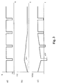
- Figure 3-a shows the signal S present at the output of the line receiver 1 where the received data correspond to a series of complete frames of consecutive ones, the length of each frame being approximately 500 ⁇ s.
- Figure 3-b) shows the development of the voltage across the capacitor C of the direct current decoupling circuit C,R1.
- Figure 3-c shows the development of the signal at the output of the direct current decoupling circuit C,R1, in which it can be seen how the increase in capacitor charge produced by the first burst is gradually compensated in tile following bursts until the same voltage is obtained on both capacitor terminals.
- This increase is measured by the control circuit 2 which generates a first control voltage Vc1 that is applied to a current generator I which, in turn, provides a suitable current to compensate the preceding increase in voltage.
- This control circuit consists of a sample and hold means 3 that samples the signal at its input in a periodic manner according to a frame clock 4 at the frame instants when no signal is being received.
- the output signal from this sample and hold means 3 is a second control signal Vc2 that is applied to a direct current adapting circuit 5 which converts this second control signal Vc2 into the first control signal Vc1 the value of which is suitable to make the current generated by the current generator I compensate the initial voltage increase.
- the direct current adapting circuit 5 is made up of a first inverter amplifier R3,R4,A2 that amplifies and inverts the second control signal Vc2 and a second inverter amplifier R5,R6,A3 that amplifies and inverts the difference between the signal coming from the first inverter amplifier R3,R4,A2 and a second reference voltage V2, producing in this way the first control signal Vc1.
- the current generator I has been designed with a PNP bipolar transistor T, the base of which receives the first control signal Vc1 and whose emitter is connected to another reference voltage V1 through a resistor R2, whereby the collector output current tends to bring the input voltage of the amplifier A1 to a value close to zero volts (reference value when no received signal), using for this the necessary number of frames.
Landscapes
- Engineering & Computer Science (AREA)
- Power Engineering (AREA)
- Optical Communication System (AREA)
- Dc Digital Transmission (AREA)
- Monitoring And Testing Of Exchanges (AREA)
- Interface Circuits In Exchanges (AREA)
Applications Claiming Priority (2)
| Application Number | Priority Date | Filing Date | Title |
|---|---|---|---|
| ES9301186 | 1993-05-31 | ||
| ES9301186A ES2076077B1 (es) | 1993-05-31 | 1993-05-31 | Circuito de control de continua en receptores de datos a rafagas. |
Publications (3)
| Publication Number | Publication Date |
|---|---|
| EP0632579A2 true EP0632579A2 (de) | 1995-01-04 |
| EP0632579A3 EP0632579A3 (de) | 1995-11-08 |
| EP0632579B1 EP0632579B1 (de) | 1999-02-24 |
Family
ID=8282006
Family Applications (1)
| Application Number | Title | Priority Date | Filing Date |
|---|---|---|---|
| EP19940107895 Expired - Lifetime EP0632579B1 (de) | 1993-05-31 | 1994-05-21 | Gleichstromsteuerungsschaltung in Burst-Datenempfängern |
Country Status (3)
| Country | Link |
|---|---|
| EP (1) | EP0632579B1 (de) |
| DE (1) | DE69416621T2 (de) |
| ES (1) | ES2076077B1 (de) |
Cited By (3)
| Publication number | Priority date | Publication date | Assignee | Title |
|---|---|---|---|---|
| WO1997008857A1 (en) * | 1995-08-24 | 1997-03-06 | British Telecommunications Public Limited Company | Burst mode optical digital receiver and repeater |
| GB2309606A (en) * | 1995-10-31 | 1997-07-30 | Plessey Semiconductors Ltd | Circuits for generating a current which is proportional to absolute temperature |
| EP1367763A1 (de) * | 2002-05-31 | 2003-12-03 | Alcatel | Verfahren der asynchronen Datenpaketübertragung sowie zugehörige Sender und Empfänger |
Family Cites Families (4)
| Publication number | Priority date | Publication date | Assignee | Title |
|---|---|---|---|---|
| US4498001A (en) * | 1982-07-26 | 1985-02-05 | At&T Bell Laboratories | Transimpedance amplifier for optical receivers |
| JPS6128208A (ja) * | 1984-07-18 | 1986-02-07 | Iwatsu Electric Co Ltd | レベル補償回路 |
| US4829594A (en) * | 1986-09-23 | 1989-05-09 | Motorola, Inc. | Adaptive correction of DC error transients |
| GB2250885B (en) * | 1990-12-13 | 1994-07-20 | Motorola Inc | Clamp circuit |
-
1993
- 1993-05-31 ES ES9301186A patent/ES2076077B1/es not_active Expired - Fee Related
-
1994
- 1994-05-21 EP EP19940107895 patent/EP0632579B1/de not_active Expired - Lifetime
- 1994-05-21 DE DE1994616621 patent/DE69416621T2/de not_active Expired - Fee Related
Cited By (5)
| Publication number | Priority date | Publication date | Assignee | Title |
|---|---|---|---|---|
| WO1997008857A1 (en) * | 1995-08-24 | 1997-03-06 | British Telecommunications Public Limited Company | Burst mode optical digital receiver and repeater |
| US6229634B1 (en) | 1995-08-24 | 2001-05-08 | British Telecommunications Public Limited Company | Burst mode optical receiver and repeater |
| GB2309606A (en) * | 1995-10-31 | 1997-07-30 | Plessey Semiconductors Ltd | Circuits for generating a current which is proportional to absolute temperature |
| EP0772111A3 (de) * | 1995-10-31 | 1998-04-15 | Plessey Semiconductors Limited | Schaltungsanordnung zur Erzeugung eines Stromes, der proportional zur absoluten Temperatur ist |
| EP1367763A1 (de) * | 2002-05-31 | 2003-12-03 | Alcatel | Verfahren der asynchronen Datenpaketübertragung sowie zugehörige Sender und Empfänger |
Also Published As
| Publication number | Publication date |
|---|---|
| ES2076077A2 (es) | 1995-10-16 |
| DE69416621T2 (de) | 1999-07-29 |
| DE69416621D1 (de) | 1999-04-01 |
| ES2076077R (de) | 1997-02-01 |
| EP0632579B1 (de) | 1999-02-24 |
| EP0632579A3 (de) | 1995-11-08 |
| ES2076077B1 (es) | 1997-08-16 |
Similar Documents
| Publication | Publication Date | Title |
|---|---|---|
| US5426389A (en) | System for DC restoration of serially transmitted binary signals | |
| US4475210A (en) | Data eye monitor | |
| US5822104A (en) | Digital optical receiving apparatus | |
| US5818378A (en) | Cable length estimation circuit using data signal edge rate detection and analog to digital conversion | |
| US4234954A (en) | On-line bit error rate estimator | |
| US8068559B1 (en) | Pulse width modulation (PWM) clock and data receiver and method for recovering information from received data signals | |
| US5050190A (en) | Signal detection circuit not affected by minute voltage fluctuations contained in input signal and operation method therefor | |
| US4097806A (en) | Adaptive equalizer with improved distortion analysis | |
| US4910753A (en) | FSK demodulating device | |
| EP0632579B1 (de) | Gleichstromsteuerungsschaltung in Burst-Datenempfängern | |
| US4423518A (en) | Timing recovery circuit | |
| JP3463727B2 (ja) | クロックパルス伝送回路 | |
| CA2045360C (en) | Signal detecting device | |
| US4833346A (en) | Switched threshold comparator for a fiber-optic receiver | |
| US6381270B1 (en) | Cable equalizer for AES digital audio data | |
| US20030231032A1 (en) | Multistage level discrimination circuit | |
| US20040208508A1 (en) | Optical signal reception control circuit and method for controlling reception of optical signal | |
| JPH0793617B2 (ja) | 位相ロックループ | |
| US5712475A (en) | Light receiving circuit with variable threshold circuit | |
| US20020140856A1 (en) | Data slicer circuit | |
| US4744093A (en) | Method of detecting phase pulse signals from an AC distribution line | |
| US4024343A (en) | Circuit arrangement for synchronizing an output signal in accordance with a periodic pulsatory input signal | |
| US4795919A (en) | Zero signal state detecting circuit | |
| US4598412A (en) | Binary digital data signal reproducing circuit in digital data transmission system | |
| EP1430314B1 (de) | Minimum detektor |
Legal Events
| Date | Code | Title | Description |
|---|---|---|---|
| PUAI | Public reference made under article 153(3) epc to a published international application that has entered the european phase |
Free format text: ORIGINAL CODE: 0009012 |
|
| AK | Designated contracting states |
Kind code of ref document: A2 Designated state(s): BE DE FR GB IT NL SE |
|
| PUAL | Search report despatched |
Free format text: ORIGINAL CODE: 0009013 |
|
| AK | Designated contracting states |
Kind code of ref document: A3 Designated state(s): BE DE FR GB IT NL SE |
|
| 17P | Request for examination filed |
Effective date: 19960422 |
|
| GRAG | Despatch of communication of intention to grant |
Free format text: ORIGINAL CODE: EPIDOS AGRA |
|
| 17Q | First examination report despatched |
Effective date: 19980514 |
|
| GRAG | Despatch of communication of intention to grant |
Free format text: ORIGINAL CODE: EPIDOS AGRA |
|
| GRAH | Despatch of communication of intention to grant a patent |
Free format text: ORIGINAL CODE: EPIDOS IGRA |
|
| GRAH | Despatch of communication of intention to grant a patent |
Free format text: ORIGINAL CODE: EPIDOS IGRA |
|
| GRAA | (expected) grant |
Free format text: ORIGINAL CODE: 0009210 |
|
| AK | Designated contracting states |
Kind code of ref document: B1 Designated state(s): BE DE FR GB IT NL SE |
|
| PG25 | Lapsed in a contracting state [announced via postgrant information from national office to epo] |
Ref country code: SE Free format text: THE PATENT HAS BEEN ANNULLED BY A DECISION OF A NATIONAL AUTHORITY Effective date: 19990224 Ref country code: NL Free format text: LAPSE BECAUSE OF FAILURE TO SUBMIT A TRANSLATION OF THE DESCRIPTION OR TO PAY THE FEE WITHIN THE PRESCRIBED TIME-LIMIT Effective date: 19990224 Ref country code: BE Free format text: LAPSE BECAUSE OF FAILURE TO SUBMIT A TRANSLATION OF THE DESCRIPTION OR TO PAY THE FEE WITHIN THE PRESCRIBED TIME-LIMIT Effective date: 19990224 |
|
| REF | Corresponds to: |
Ref document number: 69416621 Country of ref document: DE Date of ref document: 19990401 |
|
| ITF | It: translation for a ep patent filed | ||
| ET | Fr: translation filed | ||
| NLV1 | Nl: lapsed or annulled due to failure to fulfill the requirements of art. 29p and 29m of the patents act | ||
| PLBE | No opposition filed within time limit |
Free format text: ORIGINAL CODE: 0009261 |
|
| STAA | Information on the status of an ep patent application or granted ep patent |
Free format text: STATUS: NO OPPOSITION FILED WITHIN TIME LIMIT |
|
| 26N | No opposition filed | ||
| REG | Reference to a national code |
Ref country code: GB Ref legal event code: IF02 |
|
| PGFP | Annual fee paid to national office [announced via postgrant information from national office to epo] |
Ref country code: GB Payment date: 20030428 Year of fee payment: 10 |
|
| PGFP | Annual fee paid to national office [announced via postgrant information from national office to epo] |
Ref country code: FR Payment date: 20030512 Year of fee payment: 10 |
|
| PGFP | Annual fee paid to national office [announced via postgrant information from national office to epo] |
Ref country code: DE Payment date: 20030514 Year of fee payment: 10 |
|
| PG25 | Lapsed in a contracting state [announced via postgrant information from national office to epo] |
Ref country code: GB Free format text: LAPSE BECAUSE OF NON-PAYMENT OF DUE FEES Effective date: 20040521 |
|
| PG25 | Lapsed in a contracting state [announced via postgrant information from national office to epo] |
Ref country code: DE Free format text: LAPSE BECAUSE OF NON-PAYMENT OF DUE FEES Effective date: 20041201 |
|
| GBPC | Gb: european patent ceased through non-payment of renewal fee |
Effective date: 20040521 |
|
| PG25 | Lapsed in a contracting state [announced via postgrant information from national office to epo] |
Ref country code: FR Free format text: LAPSE BECAUSE OF NON-PAYMENT OF DUE FEES Effective date: 20050131 |
|
| REG | Reference to a national code |
Ref country code: FR Ref legal event code: ST |
|
| PG25 | Lapsed in a contracting state [announced via postgrant information from national office to epo] |
Ref country code: IT Free format text: LAPSE BECAUSE OF NON-PAYMENT OF DUE FEES;WARNING: LAPSES OF ITALIAN PATENTS WITH EFFECTIVE DATE BEFORE 2007 MAY HAVE OCCURRED AT ANY TIME BEFORE 2007. THE CORRECT EFFECTIVE DATE MAY BE DIFFERENT FROM THE ONE RECORDED. Effective date: 20050521 |