EP0632937B1 - Gleichstrom-Wechselstrom Versorgung - Google Patents
Gleichstrom-Wechselstrom Versorgung Download PDFInfo
- Publication number
- EP0632937B1 EP0632937B1 EP92914556A EP92914556A EP0632937B1 EP 0632937 B1 EP0632937 B1 EP 0632937B1 EP 92914556 A EP92914556 A EP 92914556A EP 92914556 A EP92914556 A EP 92914556A EP 0632937 B1 EP0632937 B1 EP 0632937B1
- Authority
- EP
- European Patent Office
- Prior art keywords
- frequency
- push
- power
- pull
- loop
- Prior art date
- Legal status (The legal status is an assumption and is not a legal conclusion. Google has not performed a legal analysis and makes no representation as to the accuracy of the status listed.)
- Expired - Lifetime
Links
Images

Classifications
-
- H—ELECTRICITY
- H02—GENERATION; CONVERSION OR DISTRIBUTION OF ELECTRIC POWER
- H02M—APPARATUS FOR CONVERSION BETWEEN AC AND AC, BETWEEN AC AND DC, OR BETWEEN DC AND DC, AND FOR USE WITH MAINS OR SIMILAR POWER SUPPLY SYSTEMS; CONVERSION OF DC OR AC INPUT POWER INTO SURGE OUTPUT POWER; CONTROL OR REGULATION THEREOF
- H02M7/00—Conversion of AC power input into DC power output; Conversion of DC power input into AC power output
- H02M7/42—Conversion of DC power input into AC power output without possibility of reversal
- H02M7/44—Conversion of DC power input into AC power output without possibility of reversal by static converters
- H02M7/48—Conversion of DC power input into AC power output without possibility of reversal by static converters using discharge tubes with control electrode or semiconductor devices with control electrode
- H02M7/4807—Conversion of DC power input into AC power output without possibility of reversal by static converters using discharge tubes with control electrode or semiconductor devices with control electrode having a high frequency intermediate AC stage
-
- H—ELECTRICITY
- H02—GENERATION; CONVERSION OR DISTRIBUTION OF ELECTRIC POWER
- H02M—APPARATUS FOR CONVERSION BETWEEN AC AND AC, BETWEEN AC AND DC, OR BETWEEN DC AND DC, AND FOR USE WITH MAINS OR SIMILAR POWER SUPPLY SYSTEMS; CONVERSION OF DC OR AC INPUT POWER INTO SURGE OUTPUT POWER; CONTROL OR REGULATION THEREOF
- H02M3/00—Conversion of DC power input into DC power output
- H02M3/22—Conversion of DC power input into DC power output with intermediate conversion into AC
- H02M3/24—Conversion of DC power input into DC power output with intermediate conversion into AC by static converters
- H02M3/28—Conversion of DC power input into DC power output with intermediate conversion into AC by static converters using discharge tubes with control electrode or semiconductor devices with control electrode to produce the intermediate AC
- H02M3/325—Conversion of DC power input into DC power output with intermediate conversion into AC by static converters using discharge tubes with control electrode or semiconductor devices with control electrode to produce the intermediate AC using devices of a triode or a transistor type requiring continuous application of a control signal
- H02M3/335—Conversion of DC power input into DC power output with intermediate conversion into AC by static converters using discharge tubes with control electrode or semiconductor devices with control electrode to produce the intermediate AC using devices of a triode or a transistor type requiring continuous application of a control signal using semiconductor devices only
- H02M3/33569—Conversion of DC power input into DC power output with intermediate conversion into AC by static converters using discharge tubes with control electrode or semiconductor devices with control electrode to produce the intermediate AC using devices of a triode or a transistor type requiring continuous application of a control signal using semiconductor devices only having several active switching elements
- H02M3/33576—Conversion of DC power input into DC power output with intermediate conversion into AC by static converters using discharge tubes with control electrode or semiconductor devices with control electrode to produce the intermediate AC using devices of a triode or a transistor type requiring continuous application of a control signal using semiconductor devices only having several active switching elements having at least one active switching element at the secondary side of an isolation transformer
- H02M3/33592—Conversion of DC power input into DC power output with intermediate conversion into AC by static converters using discharge tubes with control electrode or semiconductor devices with control electrode to produce the intermediate AC using devices of a triode or a transistor type requiring continuous application of a control signal using semiconductor devices only having several active switching elements having at least one active switching element at the secondary side of an isolation transformer having a synchronous rectifier circuit or a synchronous freewheeling circuit at the secondary side of an isolation transformer
-
- H—ELECTRICITY
- H04—ELECTRIC COMMUNICATION TECHNIQUE
- H04M—TELEPHONIC COMMUNICATION
- H04M19/00—Current supply arrangements for telephone systems
- H04M19/08—Current supply arrangements for telephone systems with current supply sources at the substations
-
- Y—GENERAL TAGGING OF NEW TECHNOLOGICAL DEVELOPMENTS; GENERAL TAGGING OF CROSS-SECTIONAL TECHNOLOGIES SPANNING OVER SEVERAL SECTIONS OF THE IPC; TECHNICAL SUBJECTS COVERED BY FORMER USPC CROSS-REFERENCE ART COLLECTIONS [XRACs] AND DIGESTS
- Y02—TECHNOLOGIES OR APPLICATIONS FOR MITIGATION OR ADAPTATION AGAINST CLIMATE CHANGE
- Y02B—CLIMATE CHANGE MITIGATION TECHNOLOGIES RELATED TO BUILDINGS, e.g. HOUSING, HOUSE APPLIANCES OR RELATED END-USER APPLICATIONS
- Y02B70/00—Technologies for an efficient end-user side electric power management and consumption
- Y02B70/10—Technologies improving the efficiency by using switched-mode power supplies [SMPS], i.e. efficient power electronics conversion e.g. power factor correction or reduction of losses in power supplies or efficient standby modes
Definitions
- the present invention relates to electronic power conversion equipment. More particularly, the present invention relates to a DC to AC power supply which has particular application and suitability to remote power supply including on-demand ring voltage generation for use at remotely located subscriber interface units ("SIU") within fiber optic networks.
- SIU subscriber interface units
- Conventional telephone instruments include an incoming call annunciator: classically a bell, more recently a piezoelectric resonator.
- a wire pair extends from a telephone central office location to the service subscriber's premises.
- Central office battery voltage is typically applied to the wire pair to power the telephone service set, and an AC voltage, nominally 90 volts at 20 Hertz, is applied whenever it is appropriate to ring the telephone bell(s) of the service set(s) at the subscriber's premises, in order to signal an incoming call and induce a user to remove the handset from its cradle, known as an "off hook" condition.
- the standard telephone service set within the U.S. Bell System includes a bell call annunciator which is broadly resonant at 20 Hertz. In Europe and elsewhere, a frequency of 25 Hertz is commonly employed as the ringing frequency.
- Ringing voltage is generated at a central office in a number of ways.
- a rotary generator or ringing machine consists of a single-speed motor (either AC or DC, depending upon the local power supply). The motor rotates one or more AC generators which generate the desired ringing frequencies and voltages. Magnetic generators operating from the AC power mains have been used to generate ringing signals. Such generators employ resistors, transformers and tuned circuits of inductors and capacitors in order to develop the desired ringing signal. Vibrating reed converters have also been employed to generate ringing voltage from the 48 volt central office battery supply.
- converters have included two magnetic coils, an armature and a reed assembly mounted on a frame, and have converted the 48 volts DC into a square wave of the desired frequency for ringing.
- a filter circuit has modified the square wave to a sine wave.
- a mechanical interrupter has been employed to divide the ringing generator's signal into alternating ringing and silent periods.
- One implementation has been a motor for rotating a shaft carrying a number of cams which operate switch contacts that switch the ringing signal on and off.
- Electronic oscillators have also been employed to generate signals used for ringing. Such circuits have been used in conjunction with private branch exchanges, etc. All of the foregoing approaches have been bulky and have required significant amounts of primary operating power.
- Fiber optic networks are proliferating within telecommunications systems. Fiber optic cables are now being extended to "curbside" or within about 100 feet or so of the subscriber's premises. In fiber optic based networks, it is not possible to send central office battery or ringing signals over the fiber optic cable, and these signals must be locally generated at the SIU and delivered to the customer in an appearance functionally identical to the existing "wire plant" network capability. While small, switched mode DC to DC converters are known to be efficient in supplying power, a hitherto unsolved need has arisen for a highly compact, highly efficient DC to DC to AC power supply including an on-demand ringing voltage generator, e.g. for inclusion within an SIU of a fiber optic network.
- a general object of the present invention is to generate and put out a smooth sine wave at a selected frequency within a range of low frequencies and at high conversion efficiency and low cost in a manner which overcomes limitations and drawbacks of the prior art.
- Another general object of the present invention is to provide a power supply for a subscriber interface unit (SIU) of an optical fiber network including an on-demand ringing voltage generation apparatus for generating a sine wave power signal in a manner which overcomes limitations and drawbacks of prior approaches.
- SIU subscriber interface unit
- a more specific object of the present invention is to provide a small, compact and highly efficient power supply for an SIU of a fiber optic network which includes a very compact and efficient DC to AC ringing voltage generator for generating and putting out a ringing signal approximating a sine wave at sufficient power to operate multiple telephone instrument bells and annunciators simultaneously and with a highly efficient circuit contained in a small physical space.
- a further object of the present invention is to provide a switched mode DC to AC power supply which includes synchronous push-pull rectification to generate an AC voltage mimicking a reference AC sinewave in a manner particularly suited for use as ringing voltage for multiple telephone instruments.
- One more object of the present invention is to provide a highly efficient, externally controllable ringing voltage generator which may be turned on and off in accordance with logic control signals.
- Yet another object of the present invention is to provide a DC to AC generator so designed that a range of operating frequencies are directly obtained by adjusting the drive frequency without circuit modification, so that e.g. 20 Hertz ringing signals may be generated for SIUs in North America, while 25 Hertz ringing signals may be generated for SIUs in Europe and in other areas of the world without circuit modification or adjustment.
- Still another object of the present invention is to provide a power supply for a subscriber interface unit (SIU) of a fiber optic network which is small and efficient in size, requiring neither physically large inductors nor physically large capacitors.
- SIU subscriber interface unit
- Yet one more object of the present invention is to make use of readily available, low cost elements, particularly integrated circuit pulse width modulator integrated circuits to realize a push pull synchronous dual quadrant rectifier circuit within a switched power supply DC to AC generator.
- Still one more object of the present invention is to employ a switched DC to AC converter and synchronous push pull rectifier to generate an AC power signal closely approximating a sine wave with minimal quantization errors or discontinuities (glitches).
- Still another object of the invention is to provide a ring sync signal for the proper timing of the application to or the removal from the subscribers time of the ringing voltage. Since various voltages on the sync wave are presented by counter states either zero crossing or points before or after zero crossing are available for use in timing ring relays or other switching circuitry which applies the ringing voltage to the line. This eliminates the need for analog circuitry to accomplish this function.
- Still one more object of the present invention is to provide a switched mode power supply for supplying power to a subscriber interface unit, including low frequency AC ringing voltage, in a manner which is independent of and isolated from a primary power source which supplies primary power to the power supply.
- a DC to AC power converter for converting a DC voltage supply to an AC voltage approximating a sine wave at a first frequency F1 via a switched mode DC to DC power supply operating at a second and much higher frequency F2.
- the DC to AC power converter includes
- the DC to AC power converter further includes a synchronizing circuit for phase synchronizing operation of the power switching circuit, the push driver and the pull driver at the higher F2 frequency.
- the DC to AC power converter establishes the frequency F1 as being in a range from 10 to 50 Hertz, and operates with the frequency F2 as being in a range from 50,000 Hertz to 1,000,000 Hertz
- the DC to AC power converter is configured to operate in a flyback mode wherein energy stored in the transformer (s) when the power switching circuit is off is delivered via the push loop and the pull loop, resp., and further comprises a storage capacitor connected at the summing junction.
- the DC to AC power converter is configured to operate in a forward mode and further comprises an inductor for energy storage connected at the summing junction.
- the DC to AC power converter further includes logic a circuit connected to control operation of said power switching circuit in accordance with an externally supplied logic control signal.
- the power switching circuit includes a first pulse width modulator
- the push driver includes a second pulse width modulator
- the pull driver includes a third pulse width modulator, the first, second and third pulse width modulators being clocked by said synchronizing circuit at the F2 frequency.
- the counter is a Johnson configuration counter configured as a modulo- 10 counter having four low order inverting outputs connected to resistors extending to a common node connecting to an input of the integrator, the integrator comprises an operational amplifier including a feedback network providing a low pass filter.
- a ring sync single is connected to each of the resistors connected to the modulo- 10 outputs for the proper timing of the application to or the removal from the subscribers time of the ringing voltage.
- the power supply according to the invention may also comprise a DC to DC switch mode power supply unit, wherein the ringing voltage DC to AC switched mode generator operates in a self-oscillation mode when the source of DC primary power is first supplied to the DC to DC switch mode power supply so as to generate power for starting said main DC to DC switched mode power supply.
- the service subscriber interface unit After the service subscriber interface unit is started, it generates 3 power supply sync reference signal PSYNC which synchronizes operation of the main DC to DC switched mode power supply and the DC to AC switched mode generator and also supplies a reference waveform which is used to generate the ringing voltage sinewave.
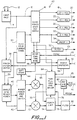
- Fig. 1 is a block diagram of a power supply incorporating the principles of the present invention, e. g. for powering a subscriber interface unit.
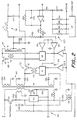
- Fig. 2 is a simplified schematic circuit diagram of a first preferred embodiment of a DC to DC to AC ring generator circuit within the Fig. 1 power supply, following a flyback configuration in accordance with principles of the present invention.
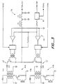
- Fig. 3 is a simplified schematic circuit diagram of a second preferred embodiment of a DC to DC to AC ring generator circuit implementing a forward mode configuration with separate power transformers and an energy storage choke in accordance with principles of the present invention.
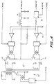
- Fig. 4 is a simplified schematic circuit diagram of a third preferred embodiment of a DC to DC to AC ring generator circuit implementing a forward mode configuration with a single power transformer and energy storage choke in accordance with principles of the present invention.
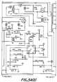
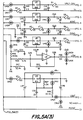
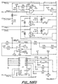
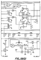
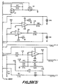
- Figs. 5A (1) to (3) and 5B (1) to 3) are a detailed circuit schematic of the Fig. 1 DC to DC to AC switch mode power supply in accordance with principles of the present invention, illustrating in detail an implementation of the Fig. 2 ring generator embodiment
- SIU subscriber interface unit
- SIU optical to electrical signal converter
- telecommunications signalling and data signals into analog control and intelligence signals, most typically voice, fax or modem signals and deliver these analog electrical signals to the subscriber over e.g. a twisted wire pair.
- the SIU is about 100 feet or so from the subscriber's premises, and is therefore necessarily a compact, highly efficient and rugged unit which may be contained in a small weather shed or protection shelter subject to the extremes of the ambient exterior environment, or which may be mounted within an equipment room at the subscriber's premises.
- the SIU must be very efficient, as the primary power supply available to it may be limited, and it must be very robust, with an expected service life free from maintenance of many years.
- a power supply 10 for an SIU (not shown) is depicted in functional and structural overview. Circuit details for one preferred implementation of this power supply 10 are provided in the circuit schematics of Figs. 5A (1)-(3) and 5B (1)-(3).
- the power supply 10, incorporating principles of the present invention efficiently converts primary DC voltage, either 48 volts or 135 volts, into a plurality of voltages, including ringing voltage, and supplies these voltages to the SIU, and through the SIU to the service subscribers via twisted pairs.
- the power supply 10 includes an on-demand ringing voltage generator in accordance with principles of the present invention.
- the ringing voltage generator synthesizes a sine wave at a sub-multiple of a ringing voltage digital driving signal, and puts out AC ringing voltage at a power level sufficient to operate up to twenty telephone bells or other annunciators simultaneously. Approximate ringing power output is 15 watts, continuous duty cycle.
- a power input 12 leads from a DC power source, either 48 volts or 135 volts DC.
- a DC power source either 48 volts or 135 volts DC.
- an external rectifier and capacitor provide the nominal 135 volts DC.
- the incoming DC voltage passes through an overvoltage surge protector array 14 which may comprise shunt and series connected metal oxide varistor (MOV) elements as conventionally employed for surge protection.
- MOV metal oxide varistor
- Surge protected power on an internal bus 15 extends to a switch mode main power supply element 16 which includes a +24 volt DC regulator 18 and +24VDC output 20, a -32 volt DC regulator 22 and -32VDC output 24, a +5 volt DC regulator 26 and +5VDC output 28, a -5 volt DC regulator 30 and -5VDC output 32 and an undervoltage detector circuit 34 which detects an undervoltage condition at the main power supply 16 and provides an alarm signal to the SIU over an output line 36.
- a +5 volts DC analog supply bus is kept separate from a +5 volts DC digital supply bus.
- the internal power bus 15 also leads to a power shutdown switch 38 which generates and supplies an enable power signal via a line 39 to a ringer power driver circuit 40.
- the ringer power driver circuit includes a pulse width modulating element which switches the DC power into alternating drive current and supplies the drive current to e.g. an enhancement mode power FET switch in series with a primary of a transformer within a ringer power transformer and switch block 42. Output from the ringer power transformer and switch block 42 is taken through a soft start block 44 to control operation of a DC/DC pulse width modulator time base generator block 46 which supplies the basic timing signals to all of the elements of the power supply 10.
- the time base generator block 46 is supplied with a reference sync signal PSYNC from the SIU over a line 48.
- the PSYNC reference signal is most preferably a logic signal approximating a square wave, and has a frequency of e.g 120 KHz to 750 KHz, and most preferably about 128 KHz.
- the time base generator block 46 applies drive to a DC/DC drive sensing circuit 50 which senses drive current applied to the main DC/DC power transformer and switch 16. PSYNC from the time base generator 46 is also supplied to the ringer power driver circuit 40.
- a filter 52 filters and puts out +5VDC digital on a line 54 to a power shutdown circuit 56 and to other digital circuitry within the power supply 10.
- Another input 58 to the power shutdown circuit 56 carries a ring enable logic signal from the SIU. This signal, as processed by the power shutdown circuit 56, causes the power shutdown switch 38 to be operated externally by the SIU, so that ringer voltage is generated only when needed, thereby conserving power.
- the DC/AC ringer power converter receives a ring frequency signal over a line 62 from the SIU, typically 200 Hz for North America, and 250Hz for Europe and other countries employing a 25 Hz ringing signal frequency.
- the ring frequency signal on the line 62 (which is a digital logic signal or square wave) is applied to a reference sine wave generator circuit 60 which generates a reference sine wave e.g. at one tenth the frequency of the ring frequency signal, in a manner which will be explained in greater detail hereinafter.
- the sine wave generator circuit 60 also generates a ring sync signal RSYNC.
- RSYNC provides a ring sync signal for the proper timing of the application to or the removal from a subscriber's time of the ringing voltage.
- the reference sine wave is also applied as a reference signal input to a dual quadrant push pull ring converter and driver 64 along with sync from the time base generator 46 and an enable signal from the power shutdown circuit 56.
- the push pull ring converter and driver 64 generates a two-quadrant push phase drive signal, and a two-quadrant pull phase drive signal and applies them to control push and pull two quadrant synchronous rectifiers.
- the plus control signal e.g. "push”
- the minus control signal e.g. pull phase
- Outputs from the push phase synchronous rectifier 68 and pull phase synchronous rectifier 72 are combined in a power combining and limiting circuit 74.
- a ringer loop feedback signal is also supplied from the output of the power limiting circuit 74 to the push pull converter and driver circuit 64 over a feedback path 76.
- the low frequency reference sinewave and the feedback signal are summed to zero and any resultant error signal controls which synchronous rectifier will be operating at any particular t i me.
- a filter 78 filters the output of the limit circuit 74 and supplies ringing current at an output 80.
- the ringing current is available selectively on demand from the SIU.
- the ringing voltage is approximately 200 Volts peak to peak, is modulated upon the -32 volt DC "central office" battery voltage put out at the output 24 by the main power supply, and thus has peak to peak excursions relative to earth ground return of +68 volts and -132 volts.
- the Fig. 1 ringer circuit comprising the elements 42, 64, 68, 72, 74 and 78, may be configured in either a flyback mode, as shown in Fig. 2 and 5A-5B, or it may be configured in a forward mode, as shown in Figs. 3 and 4, for example.
- Fig. 2 a simplified schematic of the ringing voltage generator circuit is provided. Components and elements have been given reference letters and numerals in Fig. 2 which generally correspond to the reference letters and numerals applied to the same elements in the detailed circuit schematic of Figs. 5A (1)-(3) and 5B (1)-(3).
- the driver circuit 40 includes a pulse width modulator U11 which drives an enhancement mode field effect power transistor Q5 as at a switching rate established by the PSYNC square wave driving signal, nominally 128 KHz.
- Current flowing through the primary winding of the ringing transformer T4 is sensed through the series resistor R59 and fed back to control operation of the PWM U11.
- the pulse transformer T8 and blocking capacitor C52 enable the PSYNC driving signal to be applied to operate the PWM U11.
- the function of the circuit 40 is to dump energy into the ringer power transformer T4 by causing a magnetic field to build up when the FET switch Q5 is closed.
- a feedback winding of the transformer T4 enables the switch Q5 to open and close in a free running mode when power is first applied, and before the SIU is capable of generating the PSYNC reference signal. This enables the circuit 40 to generate an initial or starting voltage supplied to the V+ bus which enables the other circuitry of the power supply 10 to begin to function in order to generate the power supplies required for operation of the SIU.
- the positive quadrants synchronous rectifier 68 includes a series loop of a T4 secondary winding, half wave diode rectifier CR7, and an enhancement mode power FET Q2 driven by a pulse transformer T2 operating in the linear mode. Direct current rectified by the diode CR7 is selectively passed by the FET Q2 and delivered to one winding of a current sense transformer T1.
- the pulse transformer T2 is driven by a pulse width modulator U2.
- the negative quadrants synchronous rectifier 72 similarly includes a series loop of another T4 secondary winding, a half wave rectifier diode CR5, and an enhancement mode power FET Q1 driven by another pulse transformer T3,
- the pulse transformer T3 is in turn driven by a pulse width modulator circuit U1.
- An analog comparator circuit comprising U5+ and U5- generates and puts out control currents to the PWMs U1 and U2 in accordance with an error signal at a summing junction labelled NODE A.
- the error signal is the difference between the reference low frequency sine wave supplied via a resistor R36 and a feedback signal supplied through a feedback resistor R35.
- the comparator U5 selects the appropriate PWM, either PWM U1 or PWM U2 to cause a signal to be passed by the respective FET switch, either Q1 or Q2, so that the voltage at the output is forced to follow the reference waveform fed into NODE A.
- the ratio of the resistors R35 and R36 establishes the voltage ratio between the reference voltage and the output voltage, and the respective resistances scale the error signal to be within the dynamic range of the comparator U5.
- the error signal tends to become positive, this will cause the positive voltage quadrants loop comprising CR7 and Q2 to turn off, and the negative quadrants loop comprising CR5 and Q1 to turn on.
- the reverse situation also obtains.
- the width of discrete pulses put out by each loop is fixed by the respective PWM U1 or U2, and has a maximum duration fixed by the PSYNC clock period.
- the control loop starting at NODE A turns on either the positive quadrants loop switch Q2 or the negative quadrants loop switch Q1 for as long as necessary to force NODE A to remain at zero volts.
- the reference sinewave generator 60 may follow a number of forms, it most preferably includes a type CD 4018 counter circuit configured as a Johnson counter in a decade arrangement.
- the modulo-10 Johnson counter architecture is a known configuration which is implemented with a shift register, and puts out essentially a Gray code in which adjacent counts result only in a single bit change.
- the following table illustrates the output pattern put out by the counter U4.
- Resistors R8 and R11 are e.g. 22 Kilohms, while resistors R7 and R9 are 33 Kilohms.
- a resistor ratio of 1/1.3 has been found to result in an output waveform from the modulo- 10 Johnson counter U4 which closely reproduces a sinewave.
- the integration capacitor C4 causes the resultant waveform put out by the counter U4 to follow a locus approximating a sinewave over four quadrants.
- An operational amplifier U6 is configured as an integrator, and it smooths the resultant sine wave and delivers it to NODE A via the resistor R36.
- RSYNC is connected to each of R8, R7, R9, and R11 to generate an appropriate ring sync.
- a negative feedback network connected across the operational amplifier U6 and comprising a 0.1 microfarad capacitor C20 and a 50 Kilohm resistor R37 establishes a low pass filter which passes signals up to about 50 Hz, but which eliminates high frequencies, including any high frequency aliases or spurs otherwise coming out of the Johnson counter U4.
- the square wave ringing reference signal entering the Johnson counter U4 is ten times the resultant sine wave, and can range from 100Hz to 500 Hz, resulting in an AC sinewave output of the ringing generator 60 of 10 Hz to 50 Hz. Differing ringing frequencies may thereby be readily generated and put out without requiring any modification or"tuning" of the ringing voltage generator circuit 60.
- the nominal ringing frequency is 20 Hz
- the reference square wave is 200 Hz
- Europe and elsewhere in the world for a 25 Hz ringing voltage, a 250 Hz reference square wave is directly applied at the ringing generator input.
- the ringing voltage transformer T4 is operated in a flyback mode wherein during the field development half cycle in which the driving circuit 40 is on, the synchronous rectifier loops 68 and 72 are biased off, and only come to life after the power driver circuit 40 has shut down.
- a filter includes an input capacitance C26, C27, and C28 followed by a relatively small smoothing choke L1 and an output capacitance C17.
- a forward mode configuration is illustrated in Fig. 3 wherein the positive quadrants loop 68' includes a driving circuit 40A, and the negative quadrants loop 72' includes a driving circuit 40B.
- the power transformers T4-A and T4-B may be made much smaller than the flyback mode transformer T4, and the drivers 40A and 40B and associated transformers T4-A and T4-B are connected so that the selected one of the diodes CR7 and CR5 will conduct on the forward or field building half cycle.
- energy storage is provided by a storage inductor LS which feeds the low pass filter 78.
- a forward mode configuration using a single transformer T4" and a single driving circuit 40" is shown in Fig. 4.
- a secondary winding and diode CR6 then provide a starting voltage V+ which is applied to start operation of a pulse width modulator U7 which in turn starts the main power supply comprising a drive transformer T5, driver FET switch Q7 and primary of main transformer T7.
- the main DC to DC converter now turns on, and generates the voltages noted in Fig. 1 and applies those voltages throughout the SIU.
- an optoisolator U9 shuts off operation of the ringer generator driver 40 by turning off the FET switch Q6.
- the SIU is receiving power, and begins to generate both the PSYNC and RINGREF square waves which are supplied back to the power supply 10.
- current demands are monitored in both the main DC to DC converter and within the ringing generator driver, and output power is controlled by the pulse width modulators U7 and U1 1.
- the laser at the SIU is dimmed, thereby extending the service life thereof.
- logic circuits U3-1, U3-3 and U3-4 cause the drivers U1 and U2 to come back to life and also turn on the switch Q6.
- the switch Q6 applies power to the ringer driver 40, and ringing voltage is generated and put out.
- the duration of the ringing voltage on interval is controlled by this logic circuitry under the direction of the SIU.
- the ringing power supply is turned on and off during each ring interval of a ringing sequence, further conserving power.
Landscapes
- Engineering & Computer Science (AREA)
- Power Engineering (AREA)
- Signal Processing (AREA)
- Devices For Supply Of Signal Current (AREA)
- Input Circuits Of Receivers And Coupling Of Receivers And Audio Equipment (AREA)
- Prostheses (AREA)
- Dc-Dc Converters (AREA)
Claims (7)
- DC zu AC Leistungswandler (10) zum Umwandeln einer Versorgungsgleichspannung in eine eine Sinusschwingung annähernde Wechselspannung mit einer ersten Frequenz F1 mittels eines DC zu DC Schaltnetzteils, das bei einer zweiten und höheren Frequenz F2 arbeitet, mit:einem Eingang (12) zum Empfangen der Versorgungsgleichspannung,einem Leistungsschaltkreis (40; 40A, 40B; 40'') zum Schalten der Versorgungsgleichspannung mit der zweiten Frequenz F2 und zum Anlegen der geschalteten Versorgungsgleichspannung an die Primärwicklungen einer oder mehrerer Transformatoren (T4; T4A, T4B; T4'') mit wenigstens einer Push-Sekundärwicklung und einer Pull-Sekundärwicklung,einer Push-Schleife (68), die die Push-Sekundärwicklung, einen Push-Gleichrichter (CR7) und einen Push-Schalter (Q2) aufweist, der bei der zweiten Frequenz F2 arbeitet,einer Pull-Schleife (72), die die Pull-Sekundärwicklung, einen Pull-Gleichrichter (CR5) und einen Pull-Schalter (Q1) aufweist, der bei der zweiten Frequenz F2 arbeitet,einer Additionsverbindung zum Addieren von Leistungen, die von der Push-Schleife (68) und von der Pull-Schleife (72) abgegeben werden und zum Bereitstellen eines Ausgangs,einer Sinusschwingung-Referenzsignal-Vorrichtung (60) zum Abgeben einer eine F1 positive Halbperiode und eine F1 negative Halbperiode aufweisende Nenn-Referenz-Sinusschwingung mit der ersten Frequenz F1, wobei die Sinusschwingung-Referenzsignal-Vorrichtung (60) aufweist:einen Referenz-Klingelsignal-Eingang zum Empfangen eines Referenz-Klingelsignals (RING REF), dessen Frequenz ein ganzzahliges Vielfaches der ersten Frequenz F1 ist,einen Zähler (U4) zum Zählen bei der Frequenz des Referenz-Klingelsignals, der eine Ausgangs-Netzwerk-Vorrichtung zum Erzeugen einer sukzessiven Näherung einer Sinusschwingung der Frequenz F1 aufweist, undeinen an den Zähler (4) angeschlossenen Integrator zum Integrieren der sukzessiven Näherung in die Nenn-Sinus-Schwingung,einem mittels der F1 positiven Halbperiode gesteuerten Push-Treiber (64) zum Steuern des Push-Schalters (Q2) bei der zweiten Frequenz F2 im wesentlichen in Übereinstimmung mit der F1 positiven Halbperiode, undeinem mittels der F1 negativen Halbperiode gesteuerten Pull-Treiber (64) zum Steuern des Pull-Schalters (Q1) bei der zweiten Frequenz F2 im wesentlichen in Übereinstimmung mit der F1 negativen Halbperiode.
- DC zu AC Leistungswandler nach Anspruch 1, ferner mit einer Synchronisations-Vorrichtung (46) zum Phasen-Synchronisations-Betrieb des Leistungsschaltkreises (40; 40A, 40B; 40'') und des Push-Treibers (64) bzw. des Pull-Treibers (64) bei der zweiten Frequenz F2.
- DC zu AC Leistungswandler nach Anspruch 1, der zum Betreiben in einem Sperrwandler-Modus ausgelegt ist, wobei Energie in dem einen oder den mehreren Transformatoren (T4) gespeichert ist, wenn der Leistungsschaltkreis (40) ausgeschaltet ist und mittels der Push-Schleife (64) bzw. der Pull-Schleife (64) abgegeben wird, und der DC zu AC Leistungswandler ferner einen Speicherkondensator (C17) aufweist, der an die Additionsverbindung angeschlossen ist.
- DC zu AC Leistungswandler nach Anspruch 1, der zum Betreiben in einem Durchflußwandler-Modus ausgelegt ist und ferner eine an die Additionsverbindung angeschlossene Induktionsspule (LS) zum Speichern von Energie und einen Logikkreis aufweist, der zum Steuern des Betriebs des Leistungsschaltkreises (40A, 40B; 40'') in Übereinstimmung mit einem von außen zugeführten Logiksteuersignal angeschlossen ist.
- DC zu AC Leistungswandler nach Anspruch 2, wobei der Leistungsschaltkreis (40; 40A, 40B; 40'') einen ersten Impulsbreitenmodulator (U11), der Push-Treiber (64) einen zweiten Impulsbreitenmodulator (U2) und der Pull-Treiber (64) einen dritten Impulsbreitenmodulator (U1) aufweisen, und der erste, der zweite und der dritte Impulsbreitenmodulator (U11, U1, U2) mittels der Synchronisationsvorrichtung (46) bei der zweiten Frequenz F2 getaktet werden.
- DC zu AC Leistungswandler nach Anspruch 1, wobei der Zähler (U4) einen Johnson-Zähler aufweist und der Integrator einen Operationsverstärker (U6) mit einem einen Tiefpaßfilter (C20, R37) aufweisenden Rückkopplungsnetzwerk umfaßt, das Referenz-Klingelsignal 10 mal F1 ist, der Johnson-Zähler als ein Modulo-10-Zähler konfiguriert ist und vier invertierende, niederwertige Ausgänge aufweist, die an Widerstände (R7, R8, R9, R10) angeschlossen sind, welche mit einem an einen Eingang des Integrators angeschlossenen gemeinsamen Knoten verbunden sind, und der eine oder die mehreren Transformatoren aus einem einzigen Transformator (T4, T4'') bestehen.
- DC zu AC Leistungswandler nach Anspruch 4, wobei der eine oder die mehreren Transformatoren einen Push-Schleifen-Transformator und einen Pull-Schleifen-Transformator aufweisen, und der Leistungsschaltkreis einen Push-Schleifen-Leistungsschaltkreis, der mit einer Primärwicklung des Push-Schleifen-Transformators verbunden ist, und einen Pull-Schleifen-Leistungsschaltkreis aufweist, der mit einer Primärwicklung des Pull-Schleifen-Transformators verbunden ist.
Priority Applications (1)
| Application Number | Priority Date | Filing Date | Title |
|---|---|---|---|
| AT92914556T ATE153485T1 (de) | 1992-03-25 | 1992-03-25 | Gleichstrom-wechselstrom versorgung |
Applications Claiming Priority (1)
| Application Number | Priority Date | Filing Date | Title |
|---|---|---|---|
| PCT/US1992/002456 WO1993019516A1 (en) | 1992-03-25 | 1992-03-25 | Dc/dc/ac power supply |
Publications (2)
| Publication Number | Publication Date |
|---|---|
| EP0632937A1 EP0632937A1 (de) | 1995-01-11 |
| EP0632937B1 true EP0632937B1 (de) | 1997-05-21 |
Family
ID=22230925
Family Applications (1)
| Application Number | Title | Priority Date | Filing Date |
|---|---|---|---|
| EP92914556A Expired - Lifetime EP0632937B1 (de) | 1992-03-25 | 1992-03-25 | Gleichstrom-Wechselstrom Versorgung |
Country Status (5)
| Country | Link |
|---|---|
| EP (1) | EP0632937B1 (de) |
| JP (1) | JPH07505031A (de) |
| AU (1) | AU667477B2 (de) |
| DE (1) | DE69219902T2 (de) |
| WO (1) | WO1993019516A1 (de) |
Families Citing this family (4)
| Publication number | Priority date | Publication date | Assignee | Title |
|---|---|---|---|---|
| DE4406500A1 (de) * | 1994-02-28 | 1995-08-31 | Siemens Ag | Schaltungsanordnung zur verlustarmen Erzeugung einer Wechselspannung |
| WO1999008371A1 (en) * | 1997-08-04 | 1999-02-18 | Koninklijke Philips Electronics N.V. | Power supply using synchronous rectification |
| US7102898B2 (en) | 2001-02-01 | 2006-09-05 | Di/Dt, Inc. | Isolated drive circuitry used in switch-mode power converters |
| JP2004536543A (ja) | 2001-02-01 | 2004-12-02 | ディーアイ/ディーティー, インコーポレーテッド | スイッチモード電力コンバータで使用される絶縁駆動回路 |
-
1992
- 1992-03-25 JP JP5516080A patent/JPH07505031A/ja active Pending
- 1992-03-25 EP EP92914556A patent/EP0632937B1/de not_active Expired - Lifetime
- 1992-03-25 DE DE69219902T patent/DE69219902T2/de not_active Expired - Fee Related
- 1992-03-25 AU AU22456/92A patent/AU667477B2/en not_active Ceased
- 1992-03-25 WO PCT/US1992/002456 patent/WO1993019516A1/en not_active Ceased
Also Published As
| Publication number | Publication date |
|---|---|
| JPH07505031A (ja) | 1995-06-01 |
| DE69219902D1 (de) | 1997-06-26 |
| AU667477B2 (en) | 1996-03-28 |
| EP0632937A1 (de) | 1995-01-11 |
| WO1993019516A1 (en) | 1993-09-30 |
| AU2245692A (en) | 1993-10-21 |
| DE69219902T2 (de) | 1998-01-08 |
Similar Documents
| Publication | Publication Date | Title |
|---|---|---|
| US5321596A (en) | DC/DC/AC power supply for a subscriber interphase unit | |
| US6049471A (en) | Controller for pulse width modulation circuit using AC sine wave from DC input signal | |
| US4803719A (en) | Method for powering telephone apparatus and telephone apparatus powered directly from the telephone line without external power | |
| US4349703A (en) | Programmable ring signal generator | |
| JPS6130963A (ja) | オフラインスイツチングモ−ド電源 | |
| CN87106586A (zh) | 产生交流电压的电路结构 | |
| US5539805A (en) | Power supply system including ringing voltage reset under low input voltage conditions | |
| JPS6130785B2 (de) | ||
| JP2000152654A (ja) | 2重出力電源及びその動作方法 | |
| US5903448A (en) | Four quadrant flyback converter, method of operation thereof and power plant employing the same | |
| EP0010900A1 (de) | Statischer Wechselrichter mit einer relativ niederfrequenten Ausgangsspannung und Verfahren zur Erzeugung dieser Spannung | |
| US3539727A (en) | Batteryless data receiver having power supply isolation between detection circuits and signal output | |
| AU667477B2 (en) | DC/DC/AC power supply | |
| US6690792B1 (en) | Active decoupling and power management circuit for line-powered ringing generator | |
| CA1075840A (en) | Circuit for interfacing an audio frequency line to a central unit | |
| CA2165591A1 (en) | Isolated high impedance, dc current sources for telecommunications applications | |
| US4648019A (en) | High efficiency ringing generator | |
| ATE242571T1 (de) | Rufsignalerzeugung in einer teilnehmerschaltung (slic) | |
| US4726060A (en) | Line circuit for driving a ringer and a service indicating lamp in a telephone set | |
| US4611097A (en) | Sine wave ring generator | |
| US4436960A (en) | Telephone ringing signal generator | |
| CA1157595A (en) | Ringing signal supply | |
| CA2107129A1 (en) | Dc/dc/ac power supply | |
| JPH0563798A (ja) | 呼出信号発生回路 | |
| US5838788A (en) | Telephone ringing signal generator |
Legal Events
| Date | Code | Title | Description |
|---|---|---|---|
| PUAI | Public reference made under article 153(3) epc to a published international application that has entered the european phase |
Free format text: ORIGINAL CODE: 0009012 |
|
| 17P | Request for examination filed |
Effective date: 19940921 |
|
| AK | Designated contracting states |
Kind code of ref document: A1 Designated state(s): AT BE CH DE DK ES FR GB GR IT LI NL SE |
|
| 17Q | First examination report despatched |
Effective date: 19950320 |
|
| GRAG | Despatch of communication of intention to grant |
Free format text: ORIGINAL CODE: EPIDOS AGRA |
|
| GRAH | Despatch of communication of intention to grant a patent |
Free format text: ORIGINAL CODE: EPIDOS IGRA |
|
| GRAH | Despatch of communication of intention to grant a patent |
Free format text: ORIGINAL CODE: EPIDOS IGRA |
|
| RTI1 | Title (correction) | ||
| GRAA | (expected) grant |
Free format text: ORIGINAL CODE: 0009210 |
|
| RAP1 | Party data changed (applicant data changed or rights of an application transferred) |
Owner name: ERICSSON RAYNET, A DELAWARE GENERAL PARTNERSHIP |
|
| AK | Designated contracting states |
Kind code of ref document: B1 Designated state(s): AT BE CH DE DK ES FR GB GR IT LI NL SE |
|
| PG25 | Lapsed in a contracting state [announced via postgrant information from national office to epo] |
Ref country code: NL Free format text: LAPSE BECAUSE OF FAILURE TO SUBMIT A TRANSLATION OF THE DESCRIPTION OR TO PAY THE FEE WITHIN THE PRESCRIBED TIME-LIMIT Effective date: 19970521 Ref country code: LI Effective date: 19970521 Ref country code: IT Free format text: LAPSE BECAUSE OF FAILURE TO SUBMIT A TRANSLATION OF THE DESCRIPTION OR TO PAY THE FEE WITHIN THE PRESCRIBED TIME-LIMIT;WARNING: LAPSES OF ITALIAN PATENTS WITH EFFECTIVE DATE BEFORE 2007 MAY HAVE OCCURRED AT ANY TIME BEFORE 2007. THE CORRECT EFFECTIVE DATE MAY BE DIFFERENT FROM THE ONE RECORDED. Effective date: 19970521 Ref country code: GR Free format text: LAPSE BECAUSE OF FAILURE TO SUBMIT A TRANSLATION OF THE DESCRIPTION OR TO PAY THE FEE WITHIN THE PRESCRIBED TIME-LIMIT Effective date: 19970521 Ref country code: FR Effective date: 19970521 Ref country code: ES Free format text: THE PATENT HAS BEEN ANNULLED BY A DECISION OF A NATIONAL AUTHORITY Effective date: 19970521 Ref country code: DK Effective date: 19970521 Ref country code: CH Effective date: 19970521 Ref country code: BE Effective date: 19970521 Ref country code: AT Effective date: 19970521 |
|
| REF | Corresponds to: |
Ref document number: 153485 Country of ref document: AT Date of ref document: 19970615 Kind code of ref document: T |
|
| REG | Reference to a national code |
Ref country code: CH Ref legal event code: EP |
|
| REF | Corresponds to: |
Ref document number: 69219902 Country of ref document: DE Date of ref document: 19970626 |
|
| PG25 | Lapsed in a contracting state [announced via postgrant information from national office to epo] |
Ref country code: SE Effective date: 19970821 |
|
| EN | Fr: translation not filed | ||
| NLV1 | Nl: lapsed or annulled due to failure to fulfill the requirements of art. 29p and 29m of the patents act | ||
| REG | Reference to a national code |
Ref country code: CH Ref legal event code: PL |
|
| PLBE | No opposition filed within time limit |
Free format text: ORIGINAL CODE: 0009261 |
|
| STAA | Information on the status of an ep patent application or granted ep patent |
Free format text: STATUS: NO OPPOSITION FILED WITHIN TIME LIMIT |
|
| 26N | No opposition filed | ||
| PGFP | Annual fee paid to national office [announced via postgrant information from national office to epo] |
Ref country code: GB Payment date: 19980616 Year of fee payment: 7 |
|
| PG25 | Lapsed in a contracting state [announced via postgrant information from national office to epo] |
Ref country code: GB Free format text: LAPSE BECAUSE OF NON-PAYMENT OF DUE FEES Effective date: 19990325 |
|
| GBPC | Gb: european patent ceased through non-payment of renewal fee |
Effective date: 19990325 |
|
| PGFP | Annual fee paid to national office [announced via postgrant information from national office to epo] |
Ref country code: DE Payment date: 20050502 Year of fee payment: 14 |
|
| PG25 | Lapsed in a contracting state [announced via postgrant information from national office to epo] |
Ref country code: DE Free format text: LAPSE BECAUSE OF NON-PAYMENT OF DUE FEES Effective date: 20061003 |