EP0633689A2 - Infrarot-Festkörperbildsensor - Google Patents
Infrarot-Festkörperbildsensor Download PDFInfo
- Publication number
- EP0633689A2 EP0633689A2 EP94107161A EP94107161A EP0633689A2 EP 0633689 A2 EP0633689 A2 EP 0633689A2 EP 94107161 A EP94107161 A EP 94107161A EP 94107161 A EP94107161 A EP 94107161A EP 0633689 A2 EP0633689 A2 EP 0633689A2
- Authority
- EP
- European Patent Office
- Prior art keywords
- charge
- horizontal
- vertical
- charge transfer
- pixel line
- Prior art date
- Legal status (The legal status is an assumption and is not a legal conclusion. Google has not performed a legal analysis and makes no representation as to the accuracy of the status listed.)
- Granted
Links
Images


Classifications
-
- H—ELECTRICITY
- H04—ELECTRIC COMMUNICATION TECHNIQUE
- H04N—PICTORIAL COMMUNICATION, e.g. TELEVISION
- H04N25/00—Circuitry of solid-state image sensors [SSIS]; Control thereof
- H04N25/70—SSIS architectures; Circuits associated therewith
- H04N25/71—Charge-coupled device [CCD] sensors; Charge-transfer registers specially adapted for CCD sensors
- H04N25/73—Charge-coupled device [CCD] sensors; Charge-transfer registers specially adapted for CCD sensors using interline transfer [IT]
-
- H—ELECTRICITY
- H04—ELECTRIC COMMUNICATION TECHNIQUE
- H04N—PICTORIAL COMMUNICATION, e.g. TELEVISION
- H04N25/00—Circuitry of solid-state image sensors [SSIS]; Control thereof
- H04N25/20—Circuitry of solid-state image sensors [SSIS]; Control thereof for transforming only infrared radiation into image signals
-
- H—ELECTRICITY
- H04—ELECTRIC COMMUNICATION TECHNIQUE
- H04N—PICTORIAL COMMUNICATION, e.g. TELEVISION
- H04N25/00—Circuitry of solid-state image sensors [SSIS]; Control thereof
- H04N25/60—Noise processing, e.g. detecting, correcting, reducing or removing noise
- H04N25/67—Noise processing, e.g. detecting, correcting, reducing or removing noise applied to fixed-pattern noise, e.g. non-uniformity of response
- H04N25/671—Noise processing, e.g. detecting, correcting, reducing or removing noise applied to fixed-pattern noise, e.g. non-uniformity of response for non-uniformity detection or correction
- H04N25/677—Noise processing, e.g. detecting, correcting, reducing or removing noise applied to fixed-pattern noise, e.g. non-uniformity of response for non-uniformity detection or correction for reducing the column or line fixed pattern noise
Definitions
- the present invention generally relates to two-dimensional solid-state image sensors, and more particularly, to an improvement of an infrared solid-state image sensor.
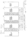
- FIG. 9 an infrared solid-state image sensor of a CSD (Charge Sweep Device) type of the prior art is shown in a schematic block diagram.
- a solid-state image sensor of the CSD type is described in detail in, for example, IEEE Journal of Solid State Circuits, Vol. SC-22, 1987, pp. 1124-1129.
- the infrared solid-state image sensor of Fig. 9 includes photodetectors 111-118, 211-218, 311-318 disposed as a two-dimensional pixel matrix in the horizontal direction and the vertical direction.
- Transfer gates 121-128, 221-228, 321-328 control transfer of signal charge from photodetectors 111-118, 211-218, 311-318 to vertical charge transfer elements 130, 230, 330, respectively.
- Storage gates 140, 240, 340 temporarily store the signal charge transferred from vertical charge transfer elements 130, 230, 330, respectively.
- Storage control gates 150, 250, 350 control transfer of signal charge from storage gates 140, 240, 340, respectively, into a horizontal charge transfer element 500.
- a preamplifier 600 provides through an output terminal 700 a voltage signal converted in proportion to an amount of signal charge provided from horizontal charge transfer element 500.
- a pixel line selecting circuit 800 is a shift register, which selects one of pixel lines in the horizontal direction (for example, lines 118, 218, 318). In Fig. 9, for simplification of the figure, connection lines relating to pixel line selecting circuit 800 are omitted.
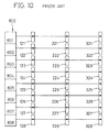
- Fig. 10 shows a connection relationship between pixel line selecting circuit 800 and transfer gates 121-128, 221-228, 321-328. Each of stages 801-808 in pixel line selecting circuit 800 is connected to a corresponding one of transfer gate lines arranged in the horizontal direction. More specifically, if, for example, pixel line selecting circuit 800 opens transfer gates 128, 228, 328 through stage 808, signal charge from photodetectors 118, 218, 318 is transferred into vertical charge transfer elements 130, 230, 330, respectively.
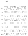
- Pixel line selecting circuit 800 generates clock signals as shown in Fig. 11. More specifically, a period from the time when the output of the nth stage of pixel line selecting circuit 800 attains an H (high) level to the time when the (n-1)th stage attains an H level is one horizontal period tH.
- One horizontal pixel line is selected for every horizontal period tH. In other words, one horizontal period corresponds to a time during which one horizontal pixel line is scanned in a solid-state image sensor.
- a vertical driving circuit 900 drives transfer of signal charge in vertical charge transfer elements 130, 230, 330.
- a connection between vertical driving circuit 900 and vertical charge transfer elements 130, 230, 330 is omitted.
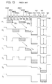
- Fig. 12 shows a connection between vertical driving circuit 900 and vertical charge transfer elements 130, 230, 330.
- Vertical charge transfer elements 130, 230, 330 include gate electrodes 131-138, 231-238, 331-338, respectively. Each of lines of these gate electrodes arranged horizontally is connected to a corresponding one of a plurality of stages 901-908 in vertical driving circuit 900. Clock signals are applied to these gate electrodes in the vertical charge transfer elements from vertical driving circuit 900.
- Fig. 13 shows potential states depending on time in a cross section taken along the line A-A of Fig. 9.
- a gate electrode 501 shown rightmost is included in a horizontal CCD (Charge Coupled Device) serving as horizontal charge transfer element 500.
- Fig. 14 is a timing chart showing clock signals applied to various gate electrodes shown in Fig. 13. More specifically, clock signals ⁇ 901- ⁇ 908 are respectively applied to gate electrodes 131-138 in vertical charge transfer element 130 from vertical driving circuit 900.
- Clock signals ⁇ ST, ⁇ SC, and ⁇ H are applied to a storage gate 140, a storage control gate 150, and a horizontal CCD gate 501, respectively.
- Potential states T1-T7 shown in Fig. 13 correspond to states at times T1-T7 shown in Fig. 14, respectively.
- potential state T1 of Fig. 13 a state immediately after transfer gate 121 is selected by pixel line selecting circuit 800, and signal charge is read out from photodetector 111 into vertical charge transfer element 130 is shown as an example. More specifically, charges QS1, QS2 are signal charges read out from photodetector 111 serving as one pixel. After being subjected to potential changes as at times T2, T3, T4, these signal charges QS1, QS2 are gathered under storage gate 140 as in a potential state shown at time T5.
- horizontal CCD 500 continues its own transfer operation.
- signal charge gathered under storage gate 140 is transferred into horizontal CCD 500 through storage control gate 150.
- signal charge from storage gate 140 as shown in a potential state at time T7 of Fig. 13 is sequentially transferred together with signal charge from other storage gates 240, 340, to be applied to preamplifier 600.
- a two-dimensional solid-state image sensor including eight pixel lines in the horizontal direction and three pixel columns in the vertical direction was described.
- a solid-state image sensor in practice generally includes several hundred horizontal pixel lines and several hundred vertical pixel columns.
- infrared image sensing is characterized by image sensing at low contrast under a high background level. Quantitative comparison of optical signal intensities in infrared image sensing and visible light image sensing is shown in, for example, IEDM Technical Digest, 1983, p. 5.
- the dark state is a state where light is not incident on a solid-state image sensor at all.
- the signal intensity is in proportion to a quantity of light on the basis of the dark state.
- Photon flux reflected from an object in the ordinary visible light image sensing is 108-1017 photon/sec ⁇ cm2, and contrast, the ratio of the signal intensity to the background level, is approximately 0.2-8.0.
- an object irradiates infrared light having an intensity depending on the temperature.
- the infrared solid-state image sensor detects infrared light irradiated depending on the temperature of the object.
- the ordinary background is in a state at room temperature, and the infrared solid-state image sensor is always subjected to a high level background radiation.
- photon flux of the background radiation is approximately 8 x 10¹⁴ photon/sec ⁇ cm2
- a change of the signal intensity corresponding to a temperature change of 1°C is only approximately 0.045 of the background level.
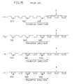
- Fig. 15 shows spreading of signal charge in the vertical charge transfer element.
- Fig. 15 (A1) signal charge immediately after being read out to a site of an arrow X from one pixel is shown by a hatched region.
- the signal charge spreads in the longitudinal direction of the vertical charge transfer element as shown in Fig. 15 (A2) to fill a plurality of potential wells. Then, the signal charge is transferred from left to right of Fig. 15.
- the signal charge in the vertical charge transfer element spreads in opposite directions along the vertical charge transfer element from a point X at which it is read out.
- Potential wells in a channel of the vertical charge transfer element are created to be as uniform as possible under respective gate electrodes.
- potential ununiformities 1310, 1320, 1330 as shown in Fig. 15 are practically generated.
- the reasons therefor are, for example, ununiformity of dimension of the channel width and variation of impurity concentration in the channel.
- ununiformity of the potential is represented by potential recessed portions 1310, 1320, 1330.
- small potential projections are sometimes generated in bottom portions of the potential wells.
- Potential recessed portions 1310, 1320, 1330 serve as signal charge traps.
- potential point-like projections do not serve as signal charge traps, a portion enclosed by a line-like projection serves as a signal charge trap.
- recessed portion 1330 traps the signal charge.
- recessed portion 1320 traps signal charge.
- recessed portions 1330, 1320, 1310 trap signal charge.
- One object of the present invention is to provide an infrared solid-state image sensor which can prevent deterioration of an image quality due to loss of transferred signal charge, even if there exists ununiformity of potential in a vertical charge transfer element.
- the infrared solid-state image sensor includes a plurality of photodetectors carrying out photoelectric conversion and charge storage as a plurality of pixels disposed in the horizontal direction and the vertical direction, pixel line selecting means for selecting at least one horizontal pixel line in one horizontal period, a plurality of vertical charge transfer elements for transferring signal charge read out from a selected pixel in the vertical direction, vertical driving means for driving the vertical charge transfer elements, and a horizontal charge transfer element for transferring signal charge from the vertical charge transfer elements in the horizontal direction, the pixel line selecting means selecting at a first time of scanning a pixel line, signal charge from which can spread to a potential well the farthest in the vertical charge transfer elements from the horizontal charge transfer element.
- the infrared solid-state image sensor includes a plurality of photodetectors for carrying out photoelectric conversion and charge storage as a plurality of pixels disposed in the horizontal direction and the vertical direction, pixel line selecting means for selecting at least one horizontal pixel line in one horizontal period, a plurality of vertical charge transfer elements for transferring signal charge from a selected pixel in the vertical direction, vertical driving means for driving the vertical charge transfer elements, and a horizontal charge transfer element for transferring signal charge from the vertical charge transfer elements in the horizontal direction, the vertical driving means controlling the vertical charge transfer elements so that they transfer signal charge in the reverse direction away from the horizontal charge transfer element at least until spreading of signal charge read out from the horizontal pixel line selected at a first time into the vertical charge transfer elements reaches a potential well the farthest from the horizontal charge transfer element, and then transfer the signal charge in the forward direction toward the horizontal charge transfer element.
- the infrared solid-state image sensor includes a plurality of photodetectors for carrying out photoelectric conversion and charge storage as a plurality of pixels disposed in the horizontal direction and the vertical direction, pixel line selecting means for selecting at least one horizontal pixel line in one horizontal period, a plurality of vertical charge transfer elements for transferring signal charge from a selected pixel in the vertical direction, vertical driving means for driving the vertical charge transfer elements, a horizontal charge transfer element for transferring signal charge from the vertical charge transfer elements in the horizontal direction, and charge input means for inputting charge to each of the vertical charge transfer elements, the charge input means inputting charge to the vertical charge transfer elements from their end portions farther from the horizontal charge transfer element at latest before a horizontal pixel line is selected at a first time of scanning.
- Fig. 1 is a schematic block diagram of an infrared solid-state image sensor according to one embodiment of the present invention.
- Fig. 2 is a diagram showing a connection between a pixel line selecting circuit and transfer gates in the infrared solid-state image sensor of Fig. 1.
- Fig. 3 is a timing chart of clock signals generated by the pixel line selecting circuit of Fig. 1.
- Fig. 4 is a schematic block diagram of an infrared solid-state image sensor according to another embodiment of the present invention.
- Fig. 5 is a timing chart of clock signals generated by a vertical driving circuit of Fig. 4.
- Fig. 6 is a schematic block diagram of an infrared solid-state image sensor according to still another embodiment of the present invention.
- Fig. 7 is a schematic block diagram of an infrared solid-state image sensor according to a further embodiment of the present invention.
- Fig. 8 is a schematic block diagram of an infrared solid-state image sensor according to a further embodiment of the present invention.
- Fig. 9 is a schematic block diagram showing one example of an infrared solid-state image sensor of the prior art.
- Fig. 10 is a diagram showing a connection between a pixel line selecting circuit and transfer gates of Fig. 9.
- Fig. 11 is a timing chart of clock signals generated by the pixel line selecting circuit of Fig. 9.
- Fig. 12 is a diagram showing a connection between a vertical driving circuit and gate electrodes in vertical charge transfer elements of Fig. 9.
- Fig. 13 is a potential diagram for explaining a charge transfer operation in the vertical charge transfer elements of Fig. 9.
- Fig. 14 is a timing chart of clock signals used for charge transfer in Fig. 13.
- Fig. 15 is a potential diagram for explaining spreading of signal charge in the vertical charge transfer elements in a conventional infrared solid-state image sensor.
- the infrared solid-state image sensor according to one embodiment of the present invention is shown in the form of a schematic block diagram. Although the infrared solid-state image sensor of Fig. 1 is similar to that of Fig. 9, a pixel line selecting circuit 810 of Fig. 1 is different from a pixel line selecting circuit 800 of Fig. 9.
- each of a plurality of stages 811-818 in pixel line selecting circuit 810 is connected to a corresponding one of transfer gate lines arranged horizontally.
- a plurality of stages 811-818 in pixel line selecting circuit 810 generates clock signals ⁇ 811- ⁇ 818 shown in Fig. 3, respectively. More specifically, in pixel line selecting circuit 810, output of the (n+1)th stage attains an H level one horizontal period after output of the nth stage attains an H level.
- a horizontal pixel line selected at a first time in each frame is the farthest from horizontal charge transfer element 500, and includes photodetectors 111, 211, 311. Signal charges read out from photodetectors 111, 211, 311 to vertical charge transfer elements 130, 230, 330, respectively, are transferred from upper ends of the vertical charge transfer elements toward lower ends close to horizontal charge transfer element 500. More specifically, signal charges from the horizontal pixel line selected at a first time are transferred through all regions of the respective vertical charge transfer elements.
- the amount of charge due to background radiation is large.
- the total amount of charge trapped in charge trap regions existing in the vertical charge transfer elements is sufficiently small compared to the amount of charge due to the background radiation. Therefore, while signal charge from the horizontal pixel line selected at a first time in each frame is transferred from upper ends to lower ends of vertical charge transfer elements 130, 230, 330, the trap regions in the vertical charge transfer elements are filled with charge. More specifically, trap regions 1310, 1320, 1330 as shown in Fig. 15, for example, are filled with charge from left in order.
- horizontal pixel lines 111, 211, 311 which are the farthest from horizontal charge transfer element 500, were selected at a first time.
- a horizontal pixel line may be selected, signal charge from which can spread to a potential well the farthest in the vertical charge transfer element from horizontal charge transfer element 500.
- the infrared solid-state image sensor according to another embodiment of the present invention is shown in a schematic block diagram.
- a vertical driving circuit 910 of Fig. 4 is different from a vertical driving circuit 900 of Fig. 9.
- Fig. 5 is a timing chart showing driving clock signals generated by vertical driving circuit 910.
- the vertical charge transfer element When the vertical charge transfer element is operated by clock shown in Fig. 9, signal charge is transferred in a direction opposite to the forward direction toward horizontal charge transfer element 500 in a period Tr, and then the signal charge is transferred in the forward direction in a following period Tf.
- the time length of the period Tr of transfer in the reverse direction is determined so that signal charge from any horizontal pixel line reaches the potential well in the vertical charge transfer element the farthest from horizontal charge transfer element 500.
- the infrared solid-state image sensor according to a still another embodiment of the present invention is shown in a schematic block diagram.
- the infrared solid-state image sensor of Fig. 6 is similar to that of Fig. 9, the infrared solid-state image sensor of Fig. 6 includes charge filling circuits 1001, 1002, 1003.
- Charge filling circuits 1001, 1002, 1003 are circuits for filling additional charge to an end the farthest from horizontal charge transfer element 500 in vertical charge transfer elements 130, 230, 330, respectively.
- a fill and spill input device can be used as shown in Optical Radiation Detectors, 1984, p.230, published by John Willy & Sons.
- a predetermined amount of charge is filled from charge filling circuits 1001, 1002, 1003 to vertical charge transfer elements 130, 230, 330, respectively, to be transferred together with signal charge.
- the filled input charge is subtracted for correction in a signal processing circuit (not shown).
- Charge filling circuits 1001, 1002, 1003 can be replaced by a horizontal input CCD 1010 as shown in Fig. 7. It will be readily understood that operations of the infrared solid-state image sensor of Fig. 7 are similar to those of Fig. 6.
- Figs. 6 and 7 the case was described where input charge is filled into the vertical charge transfer element before a horizontal pixel line is selected at a first time.
- the inputted charge may be input for every several horizontal periods or for every horizontal period. It is also possible to transfer signal charge and input charge separately from each other. In this case, the input charge may be transferred during a horizontal blanking period.
- components of input charge are not included in the output read out, it is possible to provide only components of signal charge, which in turn unnecessitates correction afterwards.
- the input charge When input charge is transferred separately from signal charge, the input charge may be transferred through horizontal charge transfer element 500 so that it will not adapted as an image signal, or a drain may be provided so that the input charge will be discarded as unnecessary charge. On the other hand, it causes no inconvenience if signal charge and input charge separately transferred in the vertical charge transfer element are mixed in storage gates 140, 240, 340. It is because the input charge can be readily subtracted for correction, as described above.
- the infrared solid-state image sensor according to a further embodiment of the present invention is shown in a schematic block diagram.
- the solid-state image sensor of Fig. 8 is similar to that of Fig. 9, the solid-state image sensor of Fig. 8 includes dummy photodetectors 119, 219, 319. Dummy photodetectors 119, 219, 319 are connected to vertical charge transfer elements 130, 230, 330 through transfer gates 129, 229, 329, respectively. Charge from each of the dummy photodetectors is filled into a site in the corresponding vertical charge transfer element the farthest from the horizontal charge transfer element. Transfer gates 119, 219, 319 for dummy detection are controlled by a clock signal ⁇ D.
- Dummy detectors 119, 219, 319 may be the same as other photodetectors used as pixels, or may be different ones.
- the clock signal ⁇ D may indicate a timing at which charge is transferred from the dummy photodetector to the vertical charge transfer element before a horizontal pixel line is selected at a first time.
- the clock signal ⁇ D may activate the transfer gate of the dummy photodetector for every predetermined horizontal periods or for every horizontal period.
- the charge trap sites due to ununiformity of the potential in the vertical charge transfer element are filled with charge, at least before second et seq. horizontal pixel lines are selected, it is possible to provide an infrared solid-state image sensor in which an image is not deteriorated due to loss of signal charge in the vertical charge transfer element.
Landscapes
- Engineering & Computer Science (AREA)
- Multimedia (AREA)
- Signal Processing (AREA)
- Transforming Light Signals Into Electric Signals (AREA)
- Solid State Image Pick-Up Elements (AREA)
Applications Claiming Priority (2)
| Application Number | Priority Date | Filing Date | Title |
|---|---|---|---|
| JP165325/93 | 1993-07-05 | ||
| JP5165325A JP3021238B2 (ja) | 1993-07-05 | 1993-07-05 | 赤外線固体撮像素子 |
Publications (3)
| Publication Number | Publication Date |
|---|---|
| EP0633689A2 true EP0633689A2 (de) | 1995-01-11 |
| EP0633689A3 EP0633689A3 (de) | 1995-02-01 |
| EP0633689B1 EP0633689B1 (de) | 1999-04-21 |
Family
ID=15810191
Family Applications (1)
| Application Number | Title | Priority Date | Filing Date |
|---|---|---|---|
| EP94107161A Expired - Lifetime EP0633689B1 (de) | 1993-07-05 | 1994-05-06 | Infrarot-Festkörperbildsensor |
Country Status (3)
| Country | Link |
|---|---|
| EP (1) | EP0633689B1 (de) |
| JP (1) | JP3021238B2 (de) |
| DE (1) | DE69417958T2 (de) |
Cited By (1)
| Publication number | Priority date | Publication date | Assignee | Title |
|---|---|---|---|---|
| EP0729268A3 (de) * | 1995-02-23 | 1997-08-20 | Mitsubishi Electric Corp | Festkörperbildaufnahmevorrichtung und Verfahren zu ihrem Betrieb |
Family Cites Families (1)
| Publication number | Priority date | Publication date | Assignee | Title |
|---|---|---|---|---|
| FR2660821A1 (fr) * | 1990-04-06 | 1991-10-11 | Thomson Csf | Matrice photosensible a transfert de charges adaptee a un balayage progressif et son procede de fabrication. |
-
1993
- 1993-07-05 JP JP5165325A patent/JP3021238B2/ja not_active Expired - Fee Related
-
1994
- 1994-05-06 DE DE69417958T patent/DE69417958T2/de not_active Expired - Fee Related
- 1994-05-06 EP EP94107161A patent/EP0633689B1/de not_active Expired - Lifetime
Cited By (1)
| Publication number | Priority date | Publication date | Assignee | Title |
|---|---|---|---|---|
| EP0729268A3 (de) * | 1995-02-23 | 1997-08-20 | Mitsubishi Electric Corp | Festkörperbildaufnahmevorrichtung und Verfahren zu ihrem Betrieb |
Also Published As
| Publication number | Publication date |
|---|---|
| EP0633689B1 (de) | 1999-04-21 |
| JP3021238B2 (ja) | 2000-03-15 |
| JPH0723301A (ja) | 1995-01-24 |
| DE69417958D1 (de) | 1999-05-27 |
| EP0633689A3 (de) | 1995-02-01 |
| DE69417958T2 (de) | 1999-10-07 |
Similar Documents
| Publication | Publication Date | Title |
|---|---|---|
| US7733401B2 (en) | Image capturing apparatus | |
| US7496291B2 (en) | Method and apparatus for interleaved image captures | |
| KR960002643B1 (ko) | 고체 촬상 소자 | |
| US6335757B1 (en) | CCD imaging device for high speed profiling | |
| EP0561599A3 (de) | Festkörperbildaufnahmevorrichtung mit automatischer Korrektur defekter Bildelemente | |
| JPH07114474B2 (ja) | 電子スチルカメラ | |
| US7675559B2 (en) | Image sensing apparatus having a two step transfer operation and method of controlling same | |
| JP2563257B2 (ja) | ビデオカメラ装置 | |
| US4821103A (en) | Solid state imaging apparatus and method with expanded dynamic range | |
| US4528595A (en) | Line transfer imager and television camera including such an imager | |
| US6778215B1 (en) | Driving method of solid-state image pickup device and image pickup system | |
| US4914493A (en) | CCD (charge coupled device) solid-state image pickup element | |
| US4661854A (en) | Transfer smear reduction for charge sweep device imagers | |
| EP0633689A2 (de) | Infrarot-Festkörperbildsensor | |
| KR19990072919A (ko) | 고체촬상장치,그구동방법및카메라 | |
| US4803555A (en) | Method of driving a solid state image pickup device | |
| JPH0575931A (ja) | 撮像装置 | |
| JP2671307B2 (ja) | 固体撮像装置 | |
| JP2895941B2 (ja) | 固体撮像装置 | |
| JP3147952B2 (ja) | 測光装置 | |
| JPS60125082A (ja) | 固体撮像装置 | |
| US20040212857A1 (en) | Control for a photosensor array | |
| JPH0622225A (ja) | Ccd撮像装置 | |
| JPS60217763A (ja) | 固体撮像装置の駆動方式 | |
| JPH06125496A (ja) | 電子スチルカメラ |
Legal Events
| Date | Code | Title | Description |
|---|---|---|---|
| PUAI | Public reference made under article 153(3) epc to a published international application that has entered the european phase |
Free format text: ORIGINAL CODE: 0009012 |
|
| PUAL | Search report despatched |
Free format text: ORIGINAL CODE: 0009013 |
|
| AK | Designated contracting states |
Kind code of ref document: A2 Designated state(s): DE FR GB |
|
| AK | Designated contracting states |
Kind code of ref document: A3 Designated state(s): DE FR GB |
|
| 17P | Request for examination filed |
Effective date: 19950306 |
|
| 17Q | First examination report despatched |
Effective date: 19970218 |
|
| GRAG | Despatch of communication of intention to grant |
Free format text: ORIGINAL CODE: EPIDOS AGRA |
|
| GRAG | Despatch of communication of intention to grant |
Free format text: ORIGINAL CODE: EPIDOS AGRA |
|
| GRAG | Despatch of communication of intention to grant |
Free format text: ORIGINAL CODE: EPIDOS AGRA |
|
| GRAH | Despatch of communication of intention to grant a patent |
Free format text: ORIGINAL CODE: EPIDOS IGRA |
|
| GRAH | Despatch of communication of intention to grant a patent |
Free format text: ORIGINAL CODE: EPIDOS IGRA |
|
| GRAH | Despatch of communication of intention to grant a patent |
Free format text: ORIGINAL CODE: EPIDOS IGRA |
|
| GRAA | (expected) grant |
Free format text: ORIGINAL CODE: 0009210 |
|
| AK | Designated contracting states |
Kind code of ref document: B1 Designated state(s): DE FR GB |
|
| REF | Corresponds to: |
Ref document number: 69417958 Country of ref document: DE Date of ref document: 19990527 |
|
| ET | Fr: translation filed | ||
| PLBE | No opposition filed within time limit |
Free format text: ORIGINAL CODE: 0009261 |
|
| STAA | Information on the status of an ep patent application or granted ep patent |
Free format text: STATUS: NO OPPOSITION FILED WITHIN TIME LIMIT |
|
| 26N | No opposition filed | ||
| REG | Reference to a national code |
Ref country code: GB Ref legal event code: IF02 |
|
| PGFP | Annual fee paid to national office [announced via postgrant information from national office to epo] |
Ref country code: GB Payment date: 20030430 Year of fee payment: 10 |
|
| PGFP | Annual fee paid to national office [announced via postgrant information from national office to epo] |
Ref country code: FR Payment date: 20030508 Year of fee payment: 10 |
|
| PGFP | Annual fee paid to national office [announced via postgrant information from national office to epo] |
Ref country code: DE Payment date: 20030515 Year of fee payment: 10 |
|
| PG25 | Lapsed in a contracting state [announced via postgrant information from national office to epo] |
Ref country code: GB Free format text: LAPSE BECAUSE OF NON-PAYMENT OF DUE FEES Effective date: 20040506 |
|
| PG25 | Lapsed in a contracting state [announced via postgrant information from national office to epo] |
Ref country code: DE Free format text: LAPSE BECAUSE OF NON-PAYMENT OF DUE FEES Effective date: 20041201 |
|
| GBPC | Gb: european patent ceased through non-payment of renewal fee |
Effective date: 20040506 |
|
| PG25 | Lapsed in a contracting state [announced via postgrant information from national office to epo] |
Ref country code: FR Free format text: LAPSE BECAUSE OF NON-PAYMENT OF DUE FEES Effective date: 20050131 |
|
| REG | Reference to a national code |
Ref country code: FR Ref legal event code: ST |