EP0634677A1 - Optische Wellenleitervorrichtung - Google Patents
Optische Wellenleitervorrichtung Download PDFInfo
- Publication number
- EP0634677A1 EP0634677A1 EP94105510A EP94105510A EP0634677A1 EP 0634677 A1 EP0634677 A1 EP 0634677A1 EP 94105510 A EP94105510 A EP 94105510A EP 94105510 A EP94105510 A EP 94105510A EP 0634677 A1 EP0634677 A1 EP 0634677A1
- Authority
- EP
- European Patent Office
- Prior art keywords
- input
- region
- output terminal
- core
- optical
- Prior art date
- Legal status (The legal status is an assumption and is not a legal conclusion. Google has not performed a legal analysis and makes no representation as to the accuracy of the status listed.)
- Ceased
Links
Images






Classifications
-
- G—PHYSICS
- G02—OPTICS
- G02B—OPTICAL ELEMENTS, SYSTEMS OR APPARATUS
- G02B6/00—Light guides; Structural details of arrangements comprising light guides and other optical elements, e.g. couplings
- G02B6/24—Coupling light guides
- G02B6/26—Optical coupling means
- G02B6/264—Optical coupling means with optical elements between opposed fibre ends which perform a function other than beam splitting
-
- G—PHYSICS
- G02—OPTICS
- G02B—OPTICAL ELEMENTS, SYSTEMS OR APPARATUS
- G02B6/00—Light guides; Structural details of arrangements comprising light guides and other optical elements, e.g. couplings
- G02B6/10—Light guides; Structural details of arrangements comprising light guides and other optical elements, e.g. couplings of the optical waveguide type
- G02B6/12—Light guides; Structural details of arrangements comprising light guides and other optical elements, e.g. couplings of the optical waveguide type of the integrated circuit kind
- G02B6/122—Basic optical elements, e.g. light-guiding paths
- G02B6/125—Bends, branchings or intersections
-
- G—PHYSICS
- G02—OPTICS
- G02B—OPTICAL ELEMENTS, SYSTEMS OR APPARATUS
- G02B6/00—Light guides; Structural details of arrangements comprising light guides and other optical elements, e.g. couplings
- G02B6/24—Coupling light guides
- G02B6/26—Optical coupling means
- G02B6/262—Optical details of coupling light into, or out of, or between fibre ends, e.g. special fibre end shapes or associated optical elements
-
- G—PHYSICS
- G02—OPTICS
- G02B—OPTICAL ELEMENTS, SYSTEMS OR APPARATUS
- G02B6/00—Light guides; Structural details of arrangements comprising light guides and other optical elements, e.g. couplings
- G02B6/24—Coupling light guides
- G02B6/26—Optical coupling means
- G02B6/28—Optical coupling means having data bus means, i.e. plural waveguides interconnected and providing an inherently bidirectional system by mixing and splitting signals
- G02B6/2804—Optical coupling means having data bus means, i.e. plural waveguides interconnected and providing an inherently bidirectional system by mixing and splitting signals forming multipart couplers without wavelength selective elements, e.g. "T" couplers, star couplers
- G02B6/2817—Optical coupling means having data bus means, i.e. plural waveguides interconnected and providing an inherently bidirectional system by mixing and splitting signals forming multipart couplers without wavelength selective elements, e.g. "T" couplers, star couplers using reflective elements to split or combine optical signals
Definitions
- the present invention relates to the structure of an optical waveguide device that functions while a functional component for performing optical branching, coupling, switching, and the like is inserted in the path of an optical waveguide and, more particularly, to a structure for facilitating manufacture of such a device which has a small transmission loss in an insertion region of the functional component.
- An optical device that performs optical branching, coupling, switching, and the like in a small region on an millimeter-order is a very important constituent element for downsizing or increasing the degree of functions of an optical communication system, an optical sensor, or the like.
- a so-called parts insertion type optical waveguide device which functions by inserting a functional component for performing optical functions such as optical branching, coupling, switching, and the like in an optical waveguide has been attracting attention in recent years.
- functions such as optical branching, coupling, and the like are conventionally realized by fabricating a directional coupler or an optical waveguide pattern having a structure of, e.g., a Y- or X-shaped waveguide, on a waveguide substrate.
- the switching function is realized by varying the propagation constant of the directional coupler.
- the functions of branching, coupling, switching and the like of the optical waveguide device can be realized by incorporating a functional component that performs branching, coupling, switching, and the like in the path of the optical waveguide formed on the waveguide substrate.
- Fig. 1 shows the arrangement of a conventional parts-insertion type optical waveguide device for realizing the optical branching function.
- a half mirror 2 serving as a functional component for separating light is inserted at the intersecting portion (an insertion region where the functional component is to be inserted) of a T-shaped optical waveguide 1.
- the half mirror 2 has an angle of 45° with respect to the optical path of the light to be incident on it.
- the core width of the optical waveguide 1 is constant (the refractive index difference between the core and the cladding layer is also constant).
- an incident side optical waveguide 1a (the incident side of the half mirror 2) is separated into a transmission-side optical waveguide 1b (the bit-side optical waveguide of the half mirror 2) and a reflection-side optical waveguide 1c (the reflection-side optical waveguide of the half mirror 2) by the half mirror 2.
- this conventional optical waveguide device The manufacturing steps of this conventional optical waveguide device will be described. Part of the intersecting portion (the insertion region where the functional component is to be inserted) of the T-shaped optical waveguide 1 formed in advance on the optical waveguide substrate (a portion indicated by a rectangle in Fig. 1) is removed with a laser beam or the like to form a space for inserting the half mirror 2 therein. Then, the half mirror 2 as the functional component is inserted.
- the conventional optical waveguide device is manufactured by performing the above manufacturing steps.
- an optical waveguide device for optical branching is as follows. Part of the intersecting portion of the T-shaped optical waveguide 1 formed in advance on the waveguide substrate where a functional component, such as a half mirror or a beam splitter, is to be inserted is removed by a laser beam process or the like. Then, the functional component for realizing a desired function is inserted in a space formed by the laser beam process or the like. Generally, a material forming the optical waveguide and the space have different refractive indices. Thus, optical diffraction occurs at this portion, causing an excessive loss. The excessive loss is a transmission loss caused by factors other than attenuation of the propagating light. If the half mirror is not inserted at a correct position, the traveling path of the light incident on this half mirror is distorted, leading to an excessive loss again.
- a functional component such as a half mirror or a beam splitter
- the process in order to correctly insert the functional component, the process must be done with a micron- or submicron-order precision.
- the countermeasure as described above for decreasing the excessive loss caused by diffraction and improving a poor parts-insertion precision is not necessary.
- this device can be manufactured easily (without requiring a high-precision process) with a good reproducibility while suppressing the transmission loss in the insertion region as compared to the conventional device.
- the optical waveguide device according to the present invention is not limited to an optical waveguide device for optical branching but can also be applied to other parts-insertion type optical waveguide devices in which a functional component for performing optical coupling, switching, and the like is inserted.
- An optical waveguide device comprises a waveguide substrate and an optical waveguide formed on the waveguide substrate and having a core for propagating light and a cladding layer covering the core.
- the optical waveguide is constituted by one or at least two optical waveguide regions serving as transmission paths of an optical signal, an insertion region having at least one input/output terminal of an optical signal and in which an optical functional component for realizing a desired function is to be inserted, and a first optical connection region having a first input/output terminal directly connected to one terminal of the optical waveguide region and a second input/output terminal directly connected to the input/output terminal of the insertion region.
- the mode field width of light propagating in the insertion region is larger than that of light at an arbitrary portion of the optical waveguide region.
- the first optical connection region has a structure for properly connecting to the optical waveguide region and the insertion region having different mode field width of light propagating therein.
- the first optical connection region has a structure for changing the mode field width of light which becomes incident from the optical waveguide region side and emerges to the insertion region side or the mode field width of light which becomes incident from the insertion region side and emerges to the optical waveguide region side.
- the core size e.g., the core width in the horizontal direction with respect to the main surface of the waveguide substrate
- the core size of the core of the first optical connection region is gradually increased from the first input/output terminal connected to the optical waveguide region toward the second input/output terminal connected to the insertion region.
- the size of the core of the first connection region is gradually decreased from the first input/output terminal connected to the optical waveguide region toward the second input/output terminal connected to the insertion region.
- the core size is set such that the core size at the first optical connection region in the vicinity of the connection surface with the insertion region becomes smaller than a core size that minimizes the mode field width of propagating light.
- the sectional shape of the core in the horizontal direction along the surface of the waveguide substrate is narrowed or widened at a predetermined taper angle in the traveling direction of light.
- the sectional shape of the core may be similar to a trapezoid.
- the optical waveguide of the optical waveguide device according to the present invention may also comprise a plurality of insertion regions.
- a second optical connection region is provided between each pair of insertion regions in order to provide a mode field width substantially the same as that of light propagating in these insertion regions.
- the second optical connection region has a core size substantially the same as that of each pair of insertion regions. The core size does not change between the incident and exit sides of light.
- a refractive index difference between the core and the cladding layer of a region where the first and/or second optical connection region directly connected to the insertion region is disposed is smaller than the refractive index difference between the core and the cladding layer at a predetermined portion of the optical waveguide region.
- Fig. 2 is a graph showing the off-axis dependency of an optical excessive loss when the optical axis of the optical waveguide in the optical waveguide device according to the present invention is deviated.
- the broken line indicates the case of an optical waveguide that sets the mode field width of propagating light to 8 ⁇ m
- the solid line indicates the case of an optical waveguide that sets the mode field width of propagating light to 18 ⁇ m.
- a spot size is a parameter two-dimensionally expressing the distribution of propagating light at a predetermined portion of the optical waveguide disposed on the waveguide substrate.
- a spot size means the size of the distribution of light having a predetermined light intensity or more at this section of the optical waveguide. More specifically, this distribution can be two-dimensionally grasped by setting the axis of abscissa as the distance from the optical axis of the core and the axis of ordinate as the light intensity.
- an area of the light distribution whose light intensity in the horizontal direction of the waveguide substrate is 1/e2 or more its peak value is defined as the mode field.
- the mode field width is uniformly defined as the maximum total width in the horizontal direction of the mode field defined in the above manner
- spot size a general parameter, can be utilized instead of the mode field width so as to express the characteristics of the present invention.
- the path of the optical waveguide for propagating light has a structure for increasing the mode field width at the insertion region where an optical functional component, such as a half mirror or a beam splitter, is inserted than a mode field width at other regions.
- an optical functional component such as a half mirror or a beam splitter
- the mode field width changes depending on the wavelength of propagating light, the refractive index difference between the core and the cladding layer of the optical waveguide, the core width, the core thickness, and the like. Therefore, the mode field width at the insertion region where the functional component is to be inserted can be increased. It might be especially effective if the core width at the input/output terminal of the insertion region is set to have a different value (larger or smaller than the width of the core at other portions) from the core width of other regions.
- connection region having a structure in which the core size (sore width) is linearly changed is provided between the first and second input/output terminals.
- Fig. 3 is a graph showing the relationship between the core width of the optical waveguide disposed on the waveguide substrate and the mode field width.
- the optical waveguide device of the example shown in Fig. 3 is manufactured by setting the optical waveguide to an SiO2-TiO2 type, the refractive index difference between the core, serving as the prospective optical waveguide, and the cladding layer to 0.3%, and the core thickness to 7 ⁇ m.
- the core width of the optical waveguide region is, e.g., 7 ⁇ m
- the mode field width of this portion is increased by increasing the core width at the insertion region to be larger than 7 ⁇ m (a range indicated by P in Fig 3).
- the core width is decreased to be smaller than a predetermined value
- the mode field width is increased as well. This is because when the core width is decreased, the optical power confinement capability of the core exceeds its limit. Therefore, in the example of Fig.
- the mode field width can be increased by decreasing the core width of the insertion region to about 2 ⁇ m (the range indicated by Q in Fig. 3) (note that all the core widths explained above are values at the core thickness of 7 ⁇ m).
- a means for decreasing the refractive index difference between the core and the cladding layer of the optical waveguide may also be employed.
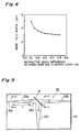
- Fig. 4 is a graph showing the relationship between the refractive index difference between the core and the cladding layer and the mode field width.
- the optical waveguide is set to an SiO2-TiO2 type, and both the width and thickness of the core serving as the prospective optical waveguide are set to 7 ⁇ m.
- the mode field width can be increased by decreasing the refractive index difference between the core and the cladding layer.
- Fig. 5 shows the arrangement of a parts-insertion type optical waveguide device having an optical branching function as a typical embodiment of the optical waveguide device according to the present invention.
- This optical waveguide device is constituted by a waveguide substrate and a T-shaped buried type SiO2-TiO2 optical waveguide 10 formed on the waveguide substrate.
- a half mirror 2 serving as an optical functional component is inserted at the intersecting portion (insertion region possibly adapted to be inserted a functional component) of the optical waveguide 10.
- a dielectric thin film may be used as the optical functional component.
- the optical waveguide 10 is constituted by at least three types of regions A, B, and C.
- the region A is an optical waveguide region having at least two input/output terminals, the region A adapted to be a light transmission path.
- the region B is a region having at least one input/output terminal of propagating light.
- This region is an insertion region possibly adapted to be inserted an optical functional component for realizing a predetermined function.
- the mode field width of light propagating in the region B is larger than that of light at a predetermined portion of the optical waveguide region.
- the region C is a region having a first input/output terminal directly connected to one input/output terminal of the optical waveguide region and a second input/output terminal directly connected to the input/output terminal of the insertion region.
- This region C is a first optical connection region for varying the mode field width of Light propagating in it.
- Each of the optical waveguide devices shown in Figs. 5, 6, and 7 has a structure for changing the mode field width of propagating light by continuously changing the core width of the first connection region C.
- the optical waveguide 10 formed on the waveguide substrate can be fabricated in accordance with sputtering, CVD, flame deposition, or the like.
- flame deposition is effective since it decreases losses.
- the manufacturing process of the SiO2-TiO2 optical waveguide 10 in accordance with flame deposition is disclosed in "Small-Loss Quartz-Based Optical Waveguide" in Optoronics (1992) No. 6, which will be summarized as follows.
- fine glass particles obtained by burning a gas mixture material of SiCl4 and TiCl4 in oxyhydrogen flame are deposited on an Si substrate (waveguide substrate) 11.
- the composition of the fine glass particles is controlled in this flame deposition process, thereby forming a two-layered fine particle film consisting of an SiO2 lower cladding layer (a layer serving as the prospective cladding layer of the optical waveguide 10) and an SiO2-TiO2 core layer (serving as the core of the optical waveguide 10).
- this two-layered fine particle film (the SiO2 lower cladding layer and the SiO2-TiO2 core layer) is heated to a high temperature of 1,000°C or more in an electric furnace to form a transparent planar optical waveguide film. Then, an unnecessary glass film portion is removed by reactive ion etching, thereby forming a ridge-shaped core.
- the core is covered with an SiO2 upper cladding layer in accordance with the flame deposition process again and changed into a transparent glass layer to form a cladding layer that constitutes the optical waveguide 10, thereby manufacturing the optical waveguide device.
- the width of the core of each connection region C is increased in the tapered manner toward the T-shaped insertion region (insertion region having three input/output terminals) of the functional component.
- the width of the core of each connection region C is decreased in the tapered manner toward the T-shaped insertion region (insertion region having three input/output terminals) of the functional component.
- a core width W1 at a portion of the optical waveguide before widened in the tapered manner, e.g., of the optical waveguide region A is, e.g., 7 ⁇ m. More specifically, this corresponds to the core width of the portion 12b indicated by the line X - X in Fig. 5.
- a core width W2 at the insertion region B is, e.g., 20 ⁇ m. More specifically, this corresponds to the core width of the portion 12a indicated by the line Y - Y in Fig. 5.
- Fig. 9 shows the sectional view of the insertion region B.
- the length of the first optical connection region C where the core width is gradually changed with a predetermined taper, angle with respect to the optical axis, i.e., a taper length L is 2 mm.
- a thickness T of the core 12a or 12b is constantly 7 ⁇ m, and the refractive index difference between the core 12a or 12b and the cladding Layer 13 is 0.3%.
- the half mirror 2 is inserted in the insertion region B which is formed to have a T shape in the optical waveguide 10.
- the half mirror 2 is mounted at an angle of 45° with respect to the optical axis of the incident light propagating through the incident-side optical waveguide 10a.
- the half mirror 2 can be mounted in accordance with various manners. Generally, a groove for inserting the half mirror is formed at a corresponding portion of the insertion region B of the optical waveguide 10 by an appropriate means, e.g., a laser beam process, chemical etching, mechanical cutting, or the like. Thereafter, the half mirror 2 is inserted in the formed groove.
- the half mirror 2 of this embodiment has a thickness of 15 ⁇ m and vertical and horizontal sides of 1 mm.
- This half mirror 2 is designed to transmit 50% and to reflect 50% of light having a wavelength of 1.31 ⁇ m.
- the core width of the core 12b in the optical waveguide region A is 7 ⁇ m and its mode field width is about 8 ⁇ m.
- the width of the core 12a at the input/output terminal of the insertion region B in the vicinity of the half mirror 2 is 20 ⁇ m. Accordingly, when light having a wavelength of 1.31 ⁇ m becomes incident on the incident-side optical waveguide 10a, the mode field of this light is enlarged in the horizontal direction as this light comes close to the half mirror 2 in the first optical connection region C.
- 50% of the incident light is guided to the transmission-side optical waveguide 10b and the remaining 50% of the incident light is guided to the reflection-side optical waveguide 10c by the half mirror 2.
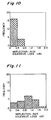
- Fig. 10 is a graph of the loss frequency distribution which evaluates an excessive loss in the reflection-side optical waveguide 10c obtained with 20 optical waveguide devices each having the above arrangement.
- Fig. 11 is a graph of the loss frequency distribution of the conventional optical waveguide device having a constant core width of 7 ⁇ m while other conditions being set to be the same as those of the above arrangement.
- the excessive loss is supposed to be caused mainly by the misalignment of the optical axis of the reflected light and the center of the core 12a of the reflection-side optical waveguide 10c due to the poor precision of the insertion position of the half mirror 2 in the manufacturing process.
- the excessive loss is smaller than that of the conventional optical waveguide device, and repeatability of the optical excessive loss is improved as well. That is, the optical waveguide device according to the present invention is less influenced by the poor insertion precision.
- the mode field width is increased by increasing the width of the core 12a at a portion corresponding to one input/output terminal of the insertion region B, where the half mirror 2 is to be inserted, to be larger than the width of the core 12b of the optical waveguide region A.
- the mode field width can be increased also by decreasing the core width.
- the core width is 7 ⁇ m in the same manner as in the above embodiment
- the mode field width can be increased by decreasing the width of the core 12a at one input/output terminal of the insertion region B, where the half mirror 2 is to be inserted, to 2 ⁇ m or less. In this case as well, the excessive loss can be decreased in the same manner as in the case wherein the core width is increased (the range Q shown in Fig. 3).
- the mode field width can be increased by decreasing the refractive index difference between the core 12a and the cladding layer 13 at one input/output terminal of the insertion region B to be smaller than the refractive index difference between the core 12b and the cladding layer 13 of the optical waveguide region A (Fig. 4).
- the refractive index of the core 12a at the insertion region B may be locally decreased. More specifically, in the case of the above embodiment, the refractive index can be decreased by diffusing TiO2 in the SiO2-TiO2 core 12a into the surrounding cladding layer 13.
- the SiO2-TiO2 optical waveguide is shown as the optical waveguide 10.
- an SiO2-GeO2 optical waveguide can also be used as a small-loss optical waveguide.
- GeO2 is diffused from a desired portion in the optical waveguide.
- the optical waveguide device in which the half mirror 2 is inserted in the T-shaped insertion region B of the optical waveguide 10 in order to provide the optical branching function has been described
- the present invention is not limited to this specific embodiment but can also be applied to other optical waveguide devices that perform optical switching, coupling, and the like.
- Fig. 12 shows data concerning an optical waveguide in which an optical waveguide region A, a first optical connection region C, an insertion region B, a first optical connection region C, and an optical waveguide region A are connected in series in the above manner.
- An optical waveguide type switch capable of linearly transmitting light or changing the traveling path of light can be manufactured by mounting the half mirrors 2, although not shown in Fig. 13, in the respective insertion regions B to be inclined at an angle of 45° with respect to the optical axes of light propagating through the corresponding optical waveguides 10, or by removing the mirrors 2.
- the present invention can also be applied to an optical waveguide device in which a filter is inserted in the optical waveguide for the purpose of selecting the wavelength of light.
- a filter When a filter is inserted, an off-axis excessive loss is rarely caused.
- the present invention can be applied to this optical waveguide device.
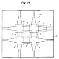
- an optical waveguide device for performing above-described optical switching, coupling, and the like which is constituted by a plurality of insertion regions B will be described (Figs. 14 and 15).
- the optical waveguide according to the present invention is formed by changing the core width in each region such that the mode field width of light propagating in each insertion region B becomes larger than that of light propagating in the corresponding optical waveguide region A. Accordingly, for the purpose of preventing an increase in excessive loss with an abrupt change in core width, the first optical connection regions C whose core width is gradually changed from the first to second input/output terminal are provided between insertion regions B and optical waveguide regions A.
- Fig. 14 shows an application of the optical waveguide device according to the present invention. Note that the insertion regions B and the first optical connection regions C may have a structure shown in Fig. 7.
- each optical waveguide 10 has an optical waveguide region A having at least two input/output terminals, the region A adapted to be a light transmission path to provide a predetermined mode field width to light.
- Each optical waveguide 10 also has an insertion region B which is a region having at least one input/output terminal of light, the region B possibly adapted to be inserted an optical functional component for realizing a predetermined function.
- the mode field width of light propagating in the insertion region B is larger than that of light propagating at a predetermined portion of the optical waveguide region A.
- Each optical waveguide 10 also has a first optical connection region C having a first input/output terminal directly connected to one input/output terminal of the optical waveguide region A and a second input/output terminal directly connected to the input/output terminal of the insertion region B for changing the mode field width of light propagating in this region.
- this optical waveguide 10 has a second optical connection region D having a first input/output terminal directly connected to the input/output terminal of one insertion region B and a second input/output terminal directly connected to the input/output terminal of the other insertion region B.
- the core sizes of the first and second input/output terminals of the second optical connection region D are equal to the core sizes of the input/output terminals of the corresponding insertion regions B to which the second optical connection region D is connected. Therefore, the mode field width of light propagating in the insertion regions B is also equal to that of light propagating in the second optical connection region D.
- the core width of the first optical connection regions C is increased before propagating light passes through the plurality of insertion regions B. That is, while the mode field width of light once increased is maintained by the second optical connection regions D, the propagating light is passed through the plurality of insertion regions B. Then, the mode field width is returned to the original size by the first optical connection regions C.
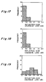
- Fig 17 is a graph showing the excessive loss frequency distribution of the first comparative example.
- Fig. 18 is a graph showing the excessive loss frequency distribution of the optical waveguide device according to the present invention.
- Fig. 19 is a graph showing the excessive loss frequency distribution of the second comparative example (conventional optical waveguide device shown in Fig. 16).
- the excessive loss is supposed to be caused mainly by the misalignment of the optical axis of the reflected light and the center of the core of the reflection-side optical waveguide due to the poor precision of the insertion position of the half mirror.
- Figs. 17 to 19 when the optical waveguide device of the first comparative example and that according to the present invention (Fig. 15) were compared with that of the second comparative example (conventional optical waveguide device), it was confirmed that the optical waveguide 10 having a tapering core at the insertion region B where the mirror 2 (optical functional component) is to be inserted had a smaller excessive loss than that of the optical waveguide 1 (second comparative example) having a constant core width, and that repeatability of the excessive loss was improved as well.
- the optical waveguide device shown in Fig. 14 can provide the same effect as that of the first comparative example while it is capable of downsizing.
- optical waveguide device shown in Fig. 5 can be applied to the optical waveguide device shown in Fig. 15.
- a connection region is provided in tight contact between the insertion region and the optical waveguide region, thereby realizing a desired function. Therefore, a transmission loss caused by insertion of the functional component can be decreased as compared to that of the conventional optical waveguide device.
- optical waveguide device can be further downsized than that of the present invention described above.
- These optical waveguide devices can be used as optical devices that are useful in downsizing and in improving the functions of an optical communication system, an optical sensor, and the like. As a result, an optical waveguide device which can be sufficiently manufactured on a mass production basis without requiring high precision can be provided.
Landscapes
- Physics & Mathematics (AREA)
- General Physics & Mathematics (AREA)
- Optics & Photonics (AREA)
- Engineering & Computer Science (AREA)
- Microelectronics & Electronic Packaging (AREA)
- Optical Integrated Circuits (AREA)
- Optical Couplings Of Light Guides (AREA)
Applications Claiming Priority (2)
| Application Number | Priority Date | Filing Date | Title |
|---|---|---|---|
| JP17697493A JPH06174954A (ja) | 1992-10-08 | 1993-07-16 | 光導波路装置 |
| JP176974/93 | 1993-07-16 |
Publications (1)
| Publication Number | Publication Date |
|---|---|
| EP0634677A1 true EP0634677A1 (de) | 1995-01-18 |
Family
ID=16022971
Family Applications (1)
| Application Number | Title | Priority Date | Filing Date |
|---|---|---|---|
| EP94105510A Ceased EP0634677A1 (de) | 1993-07-16 | 1994-04-08 | Optische Wellenleitervorrichtung |
Country Status (6)
| Country | Link |
|---|---|
| US (1) | US5438640A (de) |
| EP (1) | EP0634677A1 (de) |
| KR (1) | KR0175074B1 (de) |
| CN (1) | CN1049501C (de) |
| AU (1) | AU666257B2 (de) |
| CA (1) | CA2120792C (de) |
Cited By (3)
| Publication number | Priority date | Publication date | Assignee | Title |
|---|---|---|---|---|
| GB2300726A (en) * | 1995-05-09 | 1996-11-13 | Furukawa Electric Co Ltd | Optical waveguide wavelength division multiplexer with gap |
| EP0735350A3 (de) * | 1995-03-31 | 1997-04-09 | Yokogawa Electric Corp | Spektroskop mit faseroptischer Verzweigung |
| EP2204679A3 (de) * | 2008-12-30 | 2015-03-25 | Das Photonics, S.L. | Integrierte photonische Leiterstruktur mit Kreuzung |
Families Citing this family (20)
| Publication number | Priority date | Publication date | Assignee | Title |
|---|---|---|---|---|
| US5649037A (en) * | 1994-08-12 | 1997-07-15 | The Furukawa Electric Co., Ltd. | Optical waveguide component and a light signal processing method using the same |
| US5841933A (en) * | 1996-07-09 | 1998-11-24 | Hoaglin; Christine L. | Optical waveguide fiber containing titania and germania |
| EP0831344B1 (de) * | 1996-09-20 | 2003-02-26 | Infineon Technologies AG | Anordnung aus zwei auf der Oberfläche eines Substrates integrierten optischen Wellenleitern |
| US6785447B2 (en) * | 1998-10-09 | 2004-08-31 | Fujitsu Limited | Single and multilayer waveguides and fabrication process |
| GB2349717A (en) * | 1999-05-04 | 2000-11-08 | At & T Lab Cambridge Ltd | Low latency network |
| US20060034275A1 (en) * | 2000-05-03 | 2006-02-16 | At&T Laboratories-Cambridge Ltd. | Data transfer, synchronising applications, and low latency networks |
| DE19936187A1 (de) * | 1999-07-31 | 2001-02-01 | Daimler Chrysler Ag | Vorrichtung zur Umlenkung optischer Signale in Wellenleitern |
| JP2003114336A (ja) * | 2001-10-04 | 2003-04-18 | Matsushita Electric Ind Co Ltd | 光フィルタモジュールおよびその製造方法 |
| US7577320B2 (en) * | 2001-10-26 | 2009-08-18 | Infinera Corporation | Low loss lateral optical waveguide intersections |
| KR100417002B1 (ko) * | 2002-01-14 | 2004-02-05 | 삼성전자주식회사 | 안정화 광도파로를 구비한 광세기 분할기 |
| JP3666463B2 (ja) * | 2002-03-13 | 2005-06-29 | 日本電気株式会社 | 光導波路デバイスおよび光導波路デバイスの製造方法 |
| JP4789619B2 (ja) * | 2002-11-12 | 2011-10-12 | ホーヤ コーポレイション ユーエスエイ | 光学装置および光学装置を組み込んだ光学アセンブリ |
| CN100406936C (zh) * | 2003-05-16 | 2008-07-30 | 日立化成工业株式会社 | 光导波路结构 |
| DE102009008358A1 (de) | 2008-02-19 | 2009-09-17 | Toyoda Gosei Co., Ltd., Nishikasugai | Lichtkoppler und Herstellungsverfahren für diesen |
| JP5315715B2 (ja) * | 2008-02-19 | 2013-10-16 | 豊田合成株式会社 | 光カプラ |
| EP2600180A1 (de) * | 2008-05-09 | 2013-06-05 | Hewlett-Packard Development Company, L.P. | Optische Splittervorrichtung |
| JP6971324B2 (ja) * | 2017-03-31 | 2021-11-24 | レイア、インコーポレイテッドLeia Inc. | バックライト、マルチビューディスプレイ、およびテーパ付きコリメータを使用する方法 |
| CN108415126A (zh) * | 2018-05-10 | 2018-08-17 | 南京邮电大学 | 一种2×2新型波导光开关 |
| EP4053608A4 (de) * | 2019-10-31 | 2023-11-29 | Kyocera Corporation | Gehäuse für optische wellenleiter und lichtemittierende vorrichtung |
| KR102522558B1 (ko) * | 2022-12-26 | 2023-04-17 | (주)대진에스앤티 | 고무액이 침지된 부직포시트 제조방법 |
Citations (5)
| Publication number | Priority date | Publication date | Assignee | Title |
|---|---|---|---|---|
| GB2213954A (en) * | 1987-12-23 | 1989-08-23 | British Telecomm | Optical waveguide connecting component having tapered core |
| EP0411607A2 (de) * | 1989-08-01 | 1991-02-06 | Sumitomo Electric Industries, Ltd. | In einer optischen Faser eingebettete optische Komponente |
| EP0509236A1 (de) * | 1991-03-12 | 1992-10-21 | Canon Kabushiki Kaisha | Optischer Baustein mit optischem Koppler zum Aufspalten oder Zusammenführen von Licht und Verfahren zu dessen Herstellung |
| EP0519475A1 (de) * | 1991-06-21 | 1992-12-23 | Canon Kabushiki Kaisha | Optische Vorrichtung mit einem optischen Koppler zum Verzweigen/Kombinieren und mit einem optischen Verstärker |
| EP0530915A1 (de) * | 1991-09-02 | 1993-03-10 | Koninklijke Philips Electronics N.V. | Telekommunikationsnetzwerk mit einem einzigen Glasfaserkabel |
Family Cites Families (6)
| Publication number | Priority date | Publication date | Assignee | Title |
|---|---|---|---|---|
| US3870396A (en) * | 1973-07-05 | 1975-03-11 | Corning Glass Works | Optical coupler |
| CH591097A5 (de) * | 1975-03-18 | 1977-09-15 | Int Standard Electric Corp | |
| DE2930681A1 (de) * | 1979-07-28 | 1981-02-12 | Licentia Gmbh | Anordnung zum filtern, verzweigen, schalten oder modulieren von signalen in vielwelligen optischen wellenleitern |
| GB8429430D0 (en) * | 1984-11-21 | 1985-01-03 | Gen Electric Co Plc | Optical couplers |
| JP3031426B2 (ja) * | 1990-04-16 | 2000-04-10 | 日本電信電話株式会社 | 導波型光分岐素子 |
| DE4120208A1 (de) * | 1991-06-19 | 1992-12-24 | Buehler Edmund Gmbh & Co | Entnahmevorrichtung fuer proben, insbesondere aus einer stroemenden fluessigkeit |
-
1994
- 1994-04-07 CA CA002120792A patent/CA2120792C/en not_active Expired - Fee Related
- 1994-04-08 US US08/225,716 patent/US5438640A/en not_active Expired - Lifetime
- 1994-04-08 CN CN94105446A patent/CN1049501C/zh not_active Expired - Fee Related
- 1994-04-08 EP EP94105510A patent/EP0634677A1/de not_active Ceased
- 1994-04-08 KR KR1019940007351A patent/KR0175074B1/ko not_active Expired - Fee Related
- 1994-04-08 AU AU59367/94A patent/AU666257B2/en not_active Ceased
Patent Citations (5)
| Publication number | Priority date | Publication date | Assignee | Title |
|---|---|---|---|---|
| GB2213954A (en) * | 1987-12-23 | 1989-08-23 | British Telecomm | Optical waveguide connecting component having tapered core |
| EP0411607A2 (de) * | 1989-08-01 | 1991-02-06 | Sumitomo Electric Industries, Ltd. | In einer optischen Faser eingebettete optische Komponente |
| EP0509236A1 (de) * | 1991-03-12 | 1992-10-21 | Canon Kabushiki Kaisha | Optischer Baustein mit optischem Koppler zum Aufspalten oder Zusammenführen von Licht und Verfahren zu dessen Herstellung |
| EP0519475A1 (de) * | 1991-06-21 | 1992-12-23 | Canon Kabushiki Kaisha | Optische Vorrichtung mit einem optischen Koppler zum Verzweigen/Kombinieren und mit einem optischen Verstärker |
| EP0530915A1 (de) * | 1991-09-02 | 1993-03-10 | Koninklijke Philips Electronics N.V. | Telekommunikationsnetzwerk mit einem einzigen Glasfaserkabel |
Non-Patent Citations (1)
| Title |
|---|
| R. ZENGERLE ET AL.: "Fabrication of optical beamwidth transformers for guided waves on InP using wedge-shaped taper structures", JOURNAL OF VACUUM SCIENCE AND TECHNOLOGY: PART B, vol. B9, no. 6, December 1991 (1991-12-01), NEW YORK US, pages 3459 - 3463 * |
Cited By (5)
| Publication number | Priority date | Publication date | Assignee | Title |
|---|---|---|---|---|
| EP0735350A3 (de) * | 1995-03-31 | 1997-04-09 | Yokogawa Electric Corp | Spektroskop mit faseroptischer Verzweigung |
| GB2300726A (en) * | 1995-05-09 | 1996-11-13 | Furukawa Electric Co Ltd | Optical waveguide wavelength division multiplexer with gap |
| US5764825A (en) * | 1995-05-09 | 1998-06-09 | The Furukawa Electric Co. Ltd. | Optical wavelength division multiplexer device |
| GB2300726B (en) * | 1995-05-09 | 1998-12-23 | Furukawa Electric Co Ltd | Optical wavelength division multiplexer device |
| EP2204679A3 (de) * | 2008-12-30 | 2015-03-25 | Das Photonics, S.L. | Integrierte photonische Leiterstruktur mit Kreuzung |
Also Published As
| Publication number | Publication date |
|---|---|
| US5438640A (en) | 1995-08-01 |
| KR950003843A (ko) | 1995-02-17 |
| CA2120792A1 (en) | 1995-01-17 |
| CA2120792C (en) | 2006-05-09 |
| AU5936794A (en) | 1995-01-27 |
| AU666257B2 (en) | 1996-02-01 |
| CN1049501C (zh) | 2000-02-16 |
| CN1103719A (zh) | 1995-06-14 |
| KR0175074B1 (ko) | 1999-05-01 |
Similar Documents
| Publication | Publication Date | Title |
|---|---|---|
| US5438640A (en) | Optical waveguide device for receiving functional component | |
| EP0281800B1 (de) | Optischer Wellenleiter und Verfahren zu seiner Herstellung | |
| US6253015B1 (en) | Planar waveguides with high refractive index | |
| US6571039B1 (en) | Optical waveguide having a weakly-confining waveguide section and a strongly-confining waveguide section optically coupled by a tapered neck | |
| JP2809517B2 (ja) | 分岐合波光導波回路 | |
| AU598129B2 (en) | Optical waveguide with reflection diffraction grating | |
| EP0322744B1 (de) | Optischer Wellenleiter | |
| EP1555551B1 (de) | Apparat zur kompakten Kupplung einer optischen Faser und eines planaren Wellenleiters | |
| US6778737B2 (en) | Optical waveguide with spot size changing core structure and method for manufacturing the same | |
| EP0484878B1 (de) | Optische Schaltung mit Y-Verzweigung | |
| US4711514A (en) | Product of and process for forming tapered waveguides | |
| EP0831345A2 (de) | Faseroptisches Gitter | |
| EP2252907A1 (de) | Transformator des optischen modus, insbesondere zur kopplung einer optischen faser und eines wellenleiters mit hohem indexkontrast | |
| JP3175814B2 (ja) | 導波形光素子及びその製造方法 | |
| US4776655A (en) | Single mode optical waveguides of rectangular cross-section | |
| EP0701150A1 (de) | Verfahren zum Herstellen von Braggreflektoren für Wellenleiter und damit erhaltene Produkte | |
| EP1258753A2 (de) | Optischer Wellenleiterschaltkreis auf der Basis von Silika und zugehöriges Herstellungsverfahren | |
| US6751391B2 (en) | Optical systems incorporating waveguides and methods of manufacture | |
| US6144780A (en) | Polymer waveguide switch and method | |
| JPH0627334A (ja) | 光導波路 | |
| US5883991A (en) | Optical waveguide circulator | |
| US7499613B2 (en) | Y branch circuit and method for manufacturing the same | |
| EP0295039A2 (de) | Optischer Wellenleiterkoppler | |
| JP4585990B2 (ja) | 導波型光回路 | |
| JPH06174954A (ja) | 光導波路装置 |
Legal Events
| Date | Code | Title | Description |
|---|---|---|---|
| PUAI | Public reference made under article 153(3) epc to a published international application that has entered the european phase |
Free format text: ORIGINAL CODE: 0009012 |
|
| AK | Designated contracting states |
Kind code of ref document: A1 Designated state(s): DE FR GB IT NL SE |
|
| 17P | Request for examination filed |
Effective date: 19950223 |
|
| 17Q | First examination report despatched |
Effective date: 19980224 |
|
| APAB | Appeal dossier modified |
Free format text: ORIGINAL CODE: EPIDOS NOAPE |
|
| APAB | Appeal dossier modified |
Free format text: ORIGINAL CODE: EPIDOS NOAPE |
|
| APAD | Appeal reference recorded |
Free format text: ORIGINAL CODE: EPIDOS REFNE |
|
| APAB | Appeal dossier modified |
Free format text: ORIGINAL CODE: EPIDOS NOAPE |
|
| STAA | Information on the status of an ep patent application or granted ep patent |
Free format text: STATUS: THE APPLICATION HAS BEEN REFUSED |
|
| 18R | Application refused |
Effective date: 19991118 |
|
| APAF | Appeal reference modified |
Free format text: ORIGINAL CODE: EPIDOSCREFNE |