EP0701150A1 - Verfahren zum Herstellen von Braggreflektoren für Wellenleiter und damit erhaltene Produkte - Google Patents
Verfahren zum Herstellen von Braggreflektoren für Wellenleiter und damit erhaltene Produkte Download PDFInfo
- Publication number
- EP0701150A1 EP0701150A1 EP95306059A EP95306059A EP0701150A1 EP 0701150 A1 EP0701150 A1 EP 0701150A1 EP 95306059 A EP95306059 A EP 95306059A EP 95306059 A EP95306059 A EP 95306059A EP 0701150 A1 EP0701150 A1 EP 0701150A1
- Authority
- EP
- European Patent Office
- Prior art keywords
- layer
- improved method
- coated
- core
- index
- Prior art date
- Legal status (The legal status is an assumption and is not a legal conclusion. Google has not performed a legal analysis and makes no representation as to the accuracy of the status listed.)
- Granted
Links
Images

Classifications
-
- G—PHYSICS
- G02—OPTICS
- G02B—OPTICAL ELEMENTS, SYSTEMS OR APPARATUS
- G02B6/00—Light guides; Structural details of arrangements comprising light guides and other optical elements, e.g. couplings
- G02B6/10—Light guides; Structural details of arrangements comprising light guides and other optical elements, e.g. couplings of the optical waveguide type
- G02B6/12—Light guides; Structural details of arrangements comprising light guides and other optical elements, e.g. couplings of the optical waveguide type of the integrated circuit kind
- G02B6/13—Integrated optical circuits characterised by the manufacturing method
-
- H—ELECTRICITY
- H10—SEMICONDUCTOR DEVICES; ELECTRIC SOLID-STATE DEVICES NOT OTHERWISE PROVIDED FOR
- H10H—INORGANIC LIGHT-EMITTING SEMICONDUCTOR DEVICES HAVING POTENTIAL BARRIERS
- H10H20/00—Individual inorganic light-emitting semiconductor devices having potential barriers, e.g. light-emitting diodes [LED]
- H10H20/80—Constructional details
-
- G—PHYSICS
- G02—OPTICS
- G02B—OPTICAL ELEMENTS, SYSTEMS OR APPARATUS
- G02B6/00—Light guides; Structural details of arrangements comprising light guides and other optical elements, e.g. couplings
- G02B6/10—Light guides; Structural details of arrangements comprising light guides and other optical elements, e.g. couplings of the optical waveguide type
- G02B6/12—Light guides; Structural details of arrangements comprising light guides and other optical elements, e.g. couplings of the optical waveguide type of the integrated circuit kind
- G02B6/122—Basic optical elements, e.g. light-guiding paths
- G02B6/124—Geodesic lenses or integrated gratings
Definitions
- This invention relates to methods for making optical devices and in particular, to a method for making Bragg reflectors for waveguides.
- the method is particularly useful for making broadband Bragg reflectors for silica waveguides.
- Optical devices composed of planar optical waveguides in various configurations have much promise for optical communications systems.
- Silica waveguides for example, have been configured into a variety of passive integrated optical circuits, and additional components have been added to make hybrid integrated circuits.
- An advantage of planar waveguides over fiber devices is that photolithography can be used to make a number of identical devices and circuits in a single processing sequence, much as electronic integrated circuits are made.
- Bragg reflector filters are useful in a variety of integrated optical circuits, including drop filters and wavelength division multiplexers and demultiplexers.
- a typical Bragg filter comprises a length of optical waveguide having periodic perturbations in its index of refraction along its length to reflect light having a wavelength of twice the perturbation spacing.
- the perturbations can take the form of physical notches in the waveguide, its cladding, or both or can be photoinduced in the guiding material.
- a waveguide Bragg reflector is made by forming periodic grooves in either the undercladding or the core, applying a high index coating on the grooved surface and selectively removing the coating from the horizontal surfaces while leaving the coating on the vertical surfaces. The waveguide is then completed.
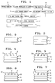
- FIG. 1 is a schematic block diagram of a preferred method for making a waveguide Bragg reflector.
- the first step shown in block A of FIG. 1 is to provide a substrate including an undercladding layer.
- the corresponding structure is schematically illustrated in FIG. 2 where the substrate 20 can be, for example, silicon or silica and the undercladding 21 is preferably silicon dioxide.
- the oxide undercladding is preferably formed by oxidation of the silicon, flame hydrolysis or low pressure chemical vapor deposition (LPCVD). Typical undercladding thicknesses are in the range 15-30 micrometers.
- the next step, shown in block B of FIG. 1, is to deposit the waveguide core layer.
- the core is preferably silica doped with phosphorus or germanium to increase its index of refraction.
- the index of the core should be higher than the index of the undercladding.
- FIG. 3 illustrates the addition of the core layer 30 on an underclad substrate. Preferred thickness of the core layer is in the range 3-9 micrometers.
- Block C of FIG. 1 shows the third step which involves forming periodic grooves in the core.
- the grooves have horizontal surfaces extending parallel to the waveguide core layer and vertical surfaces perpendicular to the core layer.
- the grooves are exposed photolithographically and etched, preferably using ion-assisted plasma etching to make substantially vertical walls.
- FIG. 4 illustrates grooves formed in the core layer 30 with vertical walls 40 and horizontal bases 41. The depth of etching is preferably in the range 0.25-1.0 micrometers.
- the periodic grooves form a corrugated grating with the etched corrugation period which is twice the desired final Bragg reflection period.
- the duty factor defined by the ratio of ridge width to the period of the corrugation is advantageously less than one.
- the next step shown in FIG. 1, block D is to coat the grooved surface with a conforming layer of high refractive index material having a thickness less than 25% of the groove width.
- the coating layer should have an index of refraction greater than the core and preferably in the range 1.8-2.5. Its thickness is advantageously less than 5% the groove width and preferably less than 1%.
- a preferred high index material is silicon nitride Si3N4 which can be applied in thin, conforming coats by LPCVD.
- FIG. 5 shows the resulting structure with high index coating 50 disposed over both the vertical walls 40 and the horizontal bases 41.
- the next step shown in FIG. 1, block E is to selectively remove the high index coating from the horizontal surfaces parallel to the core layer, while retaining the coating on the perpendicular vertical surfaces. This is advantageously accomplished by reactive ion etching.
- FIG. 6 This structure now comprises two Bragg reflectors, the first is a first order, high duty factor, high index Bragg reflector formed by the vertical sheets of the high index coating, and the second is the second order reflector formed between the oxide and the air. It is noteworthy that in the first reflector, the vertical sheets occur at twice the frequency of the grooves.
- the ridges, before coating, are slightly narrower than the troughs to account for the thickness of the coatings deposited on the walls.
- the waveguide's lateral dimension is now conveniently defined as by photolithography and reactive ion etching.
- the resulting waveguide is thus defined in both dimensions transverse to light propagation and has the Bragg reflector on the top or bottom cladding interface.
- Block G of FIG. 1 shows the final step of applying an upper cladding to fill the troughs and passivate the structure.
- the cladding is preferably boron and phosphorus doped silicon oxide deposited by LPCVD.
- the outer cladding 70 is shown deposited in FIG. 7.
- One advantage of this process is that a Bragg reflector in glass for 1.5 micrometer wavelength light can be made with half-micron resolution photolithography and filling. Half micron features can be controlled using more conventional technology without the necessity of the expense required for state-of-the-art 0.25 micron features.
- Another advantage is that vertical sheets reflect TE and TM polarizations with the same strength and wavelength dependence, so that the Bragg reflectors of sheets are nearly polarization independent, despite the high refractive index of the sheet material.
- FIG. 8 is a block diagram of the alternative process in which the first step (Block A) is provision of a substrate including an undercladding layer extending in the longitudinal direction of the waveguide to be formed.
- the second step in Block B is to etch the periodic grooves in the undercladding layer rather than the core layer.
- the next steps are to coat the grooved surface with a high index coating (Block C), to etch away the coating from the horizontal surfaces while retaining the coating on the vertical surfaces (Block D).
- the grooves are then filled with cladding material (Block E).
- the waveguide core layer can then be deposited over the filled grooves and defined in the lateral dimension (Block F), and the waveguide device can be finished in the conventional manner.
- second order Bragg reflectors with upper cladding applied were exposed and etched 1 micron deep into a lower cladding undoped oxide layer.
- the grooved surface was then coated with 230 ⁇ of Si3N4, and then vertically etched by reactive ion etching leaving Si3N4 coated sidewalls.
- the grating was then filed with boron and phosphorus doped silicon oxide (B:P:TEOS).
- B:P:TEOS boron and phosphorus doped silicon oxide
- a 3 micron phosphorus doped core layer was then deposited and the waveguide configuration was defined in a second photolithography step, leaving 2.7 x 5 micron cores.
- the entire structure was then finished with 8 microns of B:P:TEOS upper cladding. Under 1.55 micron wavelength illumination the device reflected identical modes for both TE and TM polarized light.
- FIG. 9 shows spectral reflectivity measurements made on the device diced in the middle and butted to a fiber.
- the measured external reflectivity is only 50% due to coupling loss between the fundamental modes of the fiber and the device.
- the reflection passband is nearly flat across the top which corresponds to 100% internal reflectivity of the Bragg reflector.
- the 3dB width of the reflector is 90 angstroms.
- the processing method described herein thus yield uniform, polarization independent, moderately broadband reflective filters potentially useful in many passive optical applications. Processing of these devices requires only half micron photolithographic resolution.
Landscapes
- Physics & Mathematics (AREA)
- Engineering & Computer Science (AREA)
- Microelectronics & Electronic Packaging (AREA)
- General Physics & Mathematics (AREA)
- Optics & Photonics (AREA)
- Optical Integrated Circuits (AREA)
Applications Claiming Priority (2)
| Application Number | Priority Date | Filing Date | Title |
|---|---|---|---|
| US08/303,913 US5500916A (en) | 1994-09-09 | 1994-09-09 | Method for making Bragg reflectors for waveguides |
| US303913 | 1994-09-09 |
Publications (2)
| Publication Number | Publication Date |
|---|---|
| EP0701150A1 true EP0701150A1 (de) | 1996-03-13 |
| EP0701150B1 EP0701150B1 (de) | 2003-07-23 |
Family
ID=23174245
Family Applications (1)
| Application Number | Title | Priority Date | Filing Date |
|---|---|---|---|
| EP95306059A Expired - Lifetime EP0701150B1 (de) | 1994-09-09 | 1995-08-30 | Verfahren zum Herstellen von Braggreflektoren für Wellenleiter und damit erhaltene Produkte |
Country Status (4)
| Country | Link |
|---|---|
| US (1) | US5500916A (de) |
| EP (1) | EP0701150B1 (de) |
| JP (1) | JP3613413B2 (de) |
| KR (1) | KR100384909B1 (de) |
Cited By (1)
| Publication number | Priority date | Publication date | Assignee | Title |
|---|---|---|---|---|
| US5940568A (en) * | 1996-11-19 | 1999-08-17 | Alcatel Alsthom Compagnie Generale D'electricite | Planar optical waveguide, planar optical waveguide with Bragg grating, and method of fabricating such a planar optical waveguide |
Families Citing this family (14)
| Publication number | Priority date | Publication date | Assignee | Title |
|---|---|---|---|---|
| KR100211063B1 (ko) * | 1996-12-04 | 1999-07-15 | 정선종 | 비선형 박막이 첨가된 격자-도움형 방향성 결합기 |
| US5915051A (en) * | 1997-01-21 | 1999-06-22 | Massascusetts Institute Of Technology | Wavelength-selective optical add/drop switch |
| EP1218973A4 (de) * | 1999-09-03 | 2005-11-16 | Univ California | Abstimmbare laser-quelle mit integriertem optischen modulator |
| US6628876B1 (en) * | 2000-09-15 | 2003-09-30 | Triquint Technology Holding Co. | Method for making a planar waveguide |
| US6858834B2 (en) * | 2000-10-18 | 2005-02-22 | Fibera, Inc. | Light wavelength meter |
| US6795459B2 (en) | 2000-10-18 | 2004-09-21 | Fibera, Inc. | Light frequency locker |
| US6705124B2 (en) * | 2001-06-04 | 2004-03-16 | Lightwave Microsystems Corporation | High-density plasma deposition process for fabricating a top clad for planar lightwave circuit devices |
| US6782013B2 (en) * | 2001-07-25 | 2004-08-24 | Jds Uniphase Corporation | Waveguide wavelength locker |
| US6732550B2 (en) * | 2001-09-06 | 2004-05-11 | Lightwave Microsystems, Inc. | Method for performing a deep trench etch for a planar lightwave circuit |
| US6748138B2 (en) * | 2001-09-14 | 2004-06-08 | Fibera, Inc. | Optical grating fabrication |
| US6804060B1 (en) | 2001-09-28 | 2004-10-12 | Fibera, Inc. | Interference filter fabrication |
| JP4161745B2 (ja) * | 2003-03-06 | 2008-10-08 | 株式会社デンソー | 光学素子およびその製造方法 |
| US7639911B2 (en) * | 2005-12-08 | 2009-12-29 | Electronics And Telecommunications Research Institute | Optical device having optical waveguide including organic Bragg grating sheet |
| US10753908B2 (en) * | 2017-02-22 | 2020-08-25 | The Hong Kong Polytechnic University | Resonator for force detection |
Citations (2)
| Publication number | Priority date | Publication date | Assignee | Title |
|---|---|---|---|---|
| EP0451047A1 (de) * | 1990-04-03 | 1991-10-09 | Commissariat A L'energie Atomique | Vor Umwelteinflüssen geschützte integrierte optische Komponente und Verfahren zu ihrer Herstellung |
| EP0533475A2 (de) * | 1991-09-17 | 1993-03-24 | Fujitsu Limited | Optische Halbleitervorrichtung, Verfahren zu ihrer Herstellung und aus optischen Halbleitervorrichtungen aufgebaute Laseranordnung |
Family Cites Families (9)
| Publication number | Priority date | Publication date | Assignee | Title |
|---|---|---|---|---|
| US3884549A (en) * | 1973-04-30 | 1975-05-20 | Univ California | Two demensional distributed feedback devices and lasers |
| US4464762A (en) * | 1982-02-22 | 1984-08-07 | Bell Telephone Laboratories, Incorporated | Monolithically integrated distributed Bragg reflector laser |
| US4729641A (en) * | 1983-06-10 | 1988-03-08 | Canon Kabushiki Kaisha | Functional optical element having a non-flat planar interface with variable-index medium |
| US5157537A (en) * | 1991-02-01 | 1992-10-20 | Yeda Research And Development Co., Ltd. | Distributed resonant cavity light beam modulator |
| US5367588A (en) * | 1992-10-29 | 1994-11-22 | Her Majesty The Queen In Right Of Canada, As Represented By The Minister Of Communications | Method of fabricating Bragg gratings using a silica glass phase grating mask and mask used by same |
| GB2256477B (en) * | 1991-06-07 | 1995-03-08 | Marconi Gec Ltd | An optical sensor |
| US5208882A (en) * | 1991-11-14 | 1993-05-04 | Eastman Kodak Company | Hybrid thin film optical waveguide structure having a grating coupler and a tapered waveguide film |
| US5195161A (en) * | 1991-12-11 | 1993-03-16 | At&T Bell Laboratories | Optical waveguide comprising Bragg grating coupling means |
| US5309260A (en) * | 1992-12-23 | 1994-05-03 | At&T Bell Laboratories | Method for forming distributed bragg reflectors in optical media |
-
1994
- 1994-09-09 US US08/303,913 patent/US5500916A/en not_active Expired - Lifetime
-
1995
- 1995-08-30 EP EP95306059A patent/EP0701150B1/de not_active Expired - Lifetime
- 1995-09-04 KR KR1019950028702A patent/KR100384909B1/ko not_active Expired - Lifetime
- 1995-09-08 JP JP23083495A patent/JP3613413B2/ja not_active Expired - Fee Related
Patent Citations (2)
| Publication number | Priority date | Publication date | Assignee | Title |
|---|---|---|---|---|
| EP0451047A1 (de) * | 1990-04-03 | 1991-10-09 | Commissariat A L'energie Atomique | Vor Umwelteinflüssen geschützte integrierte optische Komponente und Verfahren zu ihrer Herstellung |
| EP0533475A2 (de) * | 1991-09-17 | 1993-03-24 | Fujitsu Limited | Optische Halbleitervorrichtung, Verfahren zu ihrer Herstellung und aus optischen Halbleitervorrichtungen aufgebaute Laseranordnung |
Non-Patent Citations (1)
| Title |
|---|
| ADAR R ET AL: "POLARIZATION-INDEPENDENT BRAGG REFLECTION GRATINGS MADE WITH SILICA WAVEGUIDES ON SILICON", 2 February 1992, PROCEEDINGS OF THE OPTICAL FIBER COMMUNICATION CONFERENCE, SAN JOSE, FEB. 2 - 7, 1992, VOL. 5, PAGE(S) 260 - 261, INSTITUTE OF ELECTRICAL AND ELECTRONICS ENGINEERS * |
Cited By (1)
| Publication number | Priority date | Publication date | Assignee | Title |
|---|---|---|---|---|
| US5940568A (en) * | 1996-11-19 | 1999-08-17 | Alcatel Alsthom Compagnie Generale D'electricite | Planar optical waveguide, planar optical waveguide with Bragg grating, and method of fabricating such a planar optical waveguide |
Also Published As
| Publication number | Publication date |
|---|---|
| KR960012584A (ko) | 1996-04-20 |
| JPH0886928A (ja) | 1996-04-02 |
| EP0701150B1 (de) | 2003-07-23 |
| JP3613413B2 (ja) | 2005-01-26 |
| KR100384909B1 (ko) | 2003-08-09 |
| US5500916A (en) | 1996-03-19 |
Similar Documents
| Publication | Publication Date | Title |
|---|---|---|
| JP3581224B2 (ja) | 平面型光学導波路素子 | |
| US5500916A (en) | Method for making Bragg reflectors for waveguides | |
| US7720341B2 (en) | Waveguide for thermo optic device | |
| EP1555551B1 (de) | Apparat zur kompakten Kupplung einer optischen Faser und eines planaren Wellenleiters | |
| US8718432B1 (en) | Method for forming a spotsize converter | |
| EP0616235A1 (de) | Polarisationsunabhängige integriert optische Filter und Multiplexes | |
| US20040114899A1 (en) | Planar, integrated, optical, air-clad waveguide and method of producing same | |
| US20160246003A1 (en) | Layer Having a Non-linear Taper and Method of Fabrication | |
| US6832034B2 (en) | Optical waveguide | |
| CN100470278C (zh) | 光分路单元及其制造方法 | |
| Syms | Silica-on silicon integrated optics | |
| US20020057865A1 (en) | Optical multiplexer/demultiplexer | |
| US20050135765A1 (en) | Optical waveguide device, and method for fabricating the optical waveguide device | |
| KR20010022120A (ko) | 광소자 제조방법 및 그 광소자 | |
| JP3530463B2 (ja) | 光導波路 | |
| WO2007133915A1 (en) | Integrated optical waveguide assemblies | |
| JPH07318734A (ja) | 石英系ガラス導波路及びその製造方法 | |
| JP3602255B6 (ja) | 光反射端付きチャンネル導波路の製造方法 | |
| JP2002196170A (ja) | 光導波路の製造方法 | |
| JPH0682645A (ja) | 光方向性結合器及び光フィルタの製造方法 |
Legal Events
| Date | Code | Title | Description |
|---|---|---|---|
| PUAI | Public reference made under article 153(3) epc to a published international application that has entered the european phase |
Free format text: ORIGINAL CODE: 0009012 |
|
| AK | Designated contracting states |
Kind code of ref document: A1 Designated state(s): FR GB |
|
| 17P | Request for examination filed |
Effective date: 19960903 |
|
| 17Q | First examination report despatched |
Effective date: 20020222 |
|
| GRAH | Despatch of communication of intention to grant a patent |
Free format text: ORIGINAL CODE: EPIDOS IGRA |
|
| GRAH | Despatch of communication of intention to grant a patent |
Free format text: ORIGINAL CODE: EPIDOS IGRA |
|
| GRAA | (expected) grant |
Free format text: ORIGINAL CODE: 0009210 |
|
| AK | Designated contracting states |
Designated state(s): FR GB |
|
| REG | Reference to a national code |
Ref country code: GB Ref legal event code: FG4D |
|
| ET | Fr: translation filed | ||
| PLBE | No opposition filed within time limit |
Free format text: ORIGINAL CODE: 0009261 |
|
| STAA | Information on the status of an ep patent application or granted ep patent |
Free format text: STATUS: NO OPPOSITION FILED WITHIN TIME LIMIT |
|
| 26N | No opposition filed |
Effective date: 20040426 |
|
| PGFP | Annual fee paid to national office [announced via postgrant information from national office to epo] |
Ref country code: GB Payment date: 20130828 Year of fee payment: 19 Ref country code: FR Payment date: 20130808 Year of fee payment: 19 |
|
| GBPC | Gb: european patent ceased through non-payment of renewal fee |
Effective date: 20140830 |
|
| REG | Reference to a national code |
Ref country code: FR Ref legal event code: ST Effective date: 20150430 |
|
| PG25 | Lapsed in a contracting state [announced via postgrant information from national office to epo] |
Ref country code: GB Free format text: LAPSE BECAUSE OF NON-PAYMENT OF DUE FEES Effective date: 20140830 |
|
| PG25 | Lapsed in a contracting state [announced via postgrant information from national office to epo] |
Ref country code: FR Free format text: LAPSE BECAUSE OF NON-PAYMENT OF DUE FEES Effective date: 20140901 |