EP0635946B1 - AD-Wandler mit modulierten Rückkopplungsschleife - Google Patents
AD-Wandler mit modulierten Rückkopplungsschleife Download PDFInfo
- Publication number
- EP0635946B1 EP0635946B1 EP94401587A EP94401587A EP0635946B1 EP 0635946 B1 EP0635946 B1 EP 0635946B1 EP 94401587 A EP94401587 A EP 94401587A EP 94401587 A EP94401587 A EP 94401587A EP 0635946 B1 EP0635946 B1 EP 0635946B1
- Authority
- EP
- European Patent Office
- Prior art keywords
- signal
- analogue
- digital
- frequency
- digital converter
- Prior art date
- Legal status (The legal status is an assumption and is not a legal conclusion. Google has not performed a legal analysis and makes no representation as to the accuracy of the status listed.)
- Expired - Lifetime
Links
Images


Classifications
-
- H—ELECTRICITY
- H03—ELECTRONIC CIRCUITRY
- H03M—CODING; DECODING; CODE CONVERSION IN GENERAL
- H03M3/00—Conversion of analogue values to or from differential modulation
- H03M3/30—Delta-sigma modulation
- H03M3/39—Structural details of delta-sigma modulators, e.g. incremental delta-sigma modulators
- H03M3/402—Arrangements specific to bandpass modulators
- H03M3/41—Arrangements specific to bandpass modulators combined with modulation to or demodulation from the carrier
-
- H—ELECTRICITY
- H03—ELECTRONIC CIRCUITRY
- H03M—CODING; DECODING; CODE CONVERSION IN GENERAL
- H03M3/00—Conversion of analogue values to or from differential modulation
- H03M3/30—Delta-sigma modulation
- H03M3/39—Structural details of delta-sigma modulators, e.g. incremental delta-sigma modulators
- H03M3/412—Structural details of delta-sigma modulators, e.g. incremental delta-sigma modulators characterised by the number of quantisers and their type and resolution
- H03M3/422—Structural details of delta-sigma modulators, e.g. incremental delta-sigma modulators characterised by the number of quantisers and their type and resolution having one quantiser only
- H03M3/43—Structural details of delta-sigma modulators, e.g. incremental delta-sigma modulators characterised by the number of quantisers and their type and resolution having one quantiser only the quantiser being a single bit one
-
- H—ELECTRICITY
- H03—ELECTRONIC CIRCUITRY
- H03M—CODING; DECODING; CODE CONVERSION IN GENERAL
- H03M3/00—Conversion of analogue values to or from differential modulation
- H03M3/30—Delta-sigma modulation
- H03M3/39—Structural details of delta-sigma modulators, e.g. incremental delta-sigma modulators
- H03M3/436—Structural details of delta-sigma modulators, e.g. incremental delta-sigma modulators characterised by the order of the loop filter, e.g. error feedback type
- H03M3/456—Structural details of delta-sigma modulators, e.g. incremental delta-sigma modulators characterised by the order of the loop filter, e.g. error feedback type the modulator having a first order loop filter in the feedforward path
Definitions
- the present invention relates to a converter analog digital with modulated feedback loop.
- the field of the invention is that of conversion from an analog input signal to an output signal digital in the more precise case where this output signal must have a high resolution or when the input signal has great dynamics.
- the input signal from a receiver can vary widely, on the order of 100 dB or even more.
- the sigma-delta converter is often provided with a low-pass filtering function.
- the low-pass filter must have a cut-off frequency at least equal to f 0 + B / 2.
- f e the sampling frequency
- the converter includes also a feedback loop. This loop includes a digital to analog converter 5 which produces the reference signal Ur (t) from the deviation signal y (t). Furthermore, it is admitted here, by way of example, that the quantizer 4 produces a signal on two levels, i.e. that it is reduced to a comparator.
- the attenuation phenomenon mentioned above is particularly marked when the sampling frequency f e is less than the central frequency f 0 .
- the reference signal Ur (t) of maximum amplitude Uref is capable of changing value at the same rate as the difference signal y (t), that is to say at each sampling period Te where Te is obviously the inverse of the sampling frequency f e .
- a pulse at the output of the digital analog converter 5 thus has an amplitude Uref for a duration Te, as shown in FIG. 2A.
- the Fourier transform S (f) of the impulse response, or frequency response, represented in FIG. 2B is of the sinx / x form already mentioned because this converter 5 has a low-pass filtering function. If the center frequency f 0 is for example 2.25 times the sampling frequency f e , it appears that the attenuation is very important.
- the known solution consists in reducing the width of the impulse to approach the ideal case of the impulse from Dirac.
- the amplitude of the impetus to maintain a constant area which is worth Uref.Te.
- the Fourier transform S (f) of the impulse response, or frequency response, is shown in Figure 3B. We have reduced attenuation but this is still relatively high.
- the object of the present invention is therefore to provide an analog-to-digital converter well suited to processing a signal occupying a frequency band B less than its center frequency f 0 .
- Analog to digital converter receives signal analog input to produce a deviation signal digital. It includes a subtractor to make the difference of the input signal and a reference signal, a conversion chain to produce this deviation signal at from this difference and a feedback loop to produce the reference signal by means of a digital to analog converter which outputs a signal from comparison in response to the deviation signal.
- the input signal being assigned a central frequency
- the feedback loop further includes a displacement to displace the frequency response of the zero frequency digital to analog converter towards the central frequency, this displacement member producing the reference signal from the signal comparison.
- displacement device is a modulator producing the reference signal by modulation of the comparison signal by means of a signal modulating.
- the modulating signal has a spectral component at a modulation frequency equal to the center frequency.
- the signal is the product of the comparison signal and the modulating signal.
- the invention applies naturally when the chain conversion includes a sampler working at a sampling frequency, so the deviation signal keeps a constant value during a period sampling.
- the modulating signal has a spectral component at a frequency of modulation equal to a multiple of half of this sampling frequency.
- the modulating signal has a value positive at the end of each period of samples.
- the conversion chain includes a filter bandpass centered on the center frequency and a quantifier.
- this quantifier is a comparator.
- Sigma-delta converters are generally with two main functions: conversion proper and digital processing including including a filtering and decimation operation.
- the invention relates to the conversion proper, that is to say say the set of organs that get the deviation signal at the output of the quantizer. That is why we will now consider, through an abuse of language, that the analog to digital converter matches these only organs.
- the invention proposes to alleviate the phenomenon mitigation presented above and shown schematically in the figure 2B.
- Provision is made for this to move the main lobe of the frequency response which is the Fourier transform S (f) of the impulse response from the frequency f 0 to the central frequency f 0 by means of a displacement member.
- the sigma-delta converter includes a subtractor 1 which receives an input signal x (t) and a reference signal Ur (t) to tell the difference. It then includes a bandpass filter 2 which receives the output signal from the subtractor 1 to produce a filtered signal, a sampler 3 which receives this filtered signal and produces samples, and a quantifier 4 which delivers a signal numerical deviation y (t) from these samples.
- the quantifier 4 produces a signal on two levels, i.e. it reduced to a comparator.
- the assembly constituted by the filter 2, the sampler 3 and the quantifier 4 provide a function well known to those skilled in the art and we will agree to name it conversion chain.
- the sigma-delta converter also includes a feedback loop. This loop has a digital to analog converter 5 which produces a signal comparison Uc (t) from the deviation signal y (t).
- the feedback loop includes the displacement device which produces the signal reference Ur (t) from the comparison signal Uc (t).
- a low-pass filter can be provided 6 at the output of the digital analog converter 5.
- the function of this filter will be explained later.
- this movement member is a modulator (7) which produces the reference signal Ur (t) by modulating the comparison signal Uc (t) filtered or unfiltered by means of a modulating signal md (t).
- the modulation operation is a multiplication so the reference signal Ur (t) is the product of the comparison signal Uc (t) and the modulating signal md (t).
- the purpose of this modulation is to modify the response frequency of digital to analog converter 5.
- the modulating signal md (t) can be sinusoidal, at which the low-pass filter 6 is of more limited interest. However, it may be more convenient to choose a signal square, to facilitate the realization of modulator 7, by example.
- This modulating signal md (t) is therefore chosen so that it has a spectral component at the modulation frequency f m close to the central frequency f 0 .
- these two frequencies should be equal, but it may be more convenient to adopt different values if only for technological reasons.
- the phase of md (t) is important for the stability of the sigma-delta converter. However, the ambiguity of the phase for cases m> 0 is simple to raise, as has been approached by J.H. DRESSLER in the work already cited.
- the modulating signal m 1 (t) In the first form of the modulating signal m 1 (t), there appears a positive feedback at the end of the sampling period, that is to say between 3T / 2 and Te in the present case. This phenomenon can cause the sigma-delta converter to oscillate.
- An advantageous solution consists in choosing the second form m 2 (t) of the modulating signal to avoid any risk of instability.
- the modulating signal must always have a positive value at the end of a sampling period, that is to say during a possible change in value of the comparison signal Uc (t).
- the coefficient ⁇ and the gain a 0 are determined in order to optimize the noise rejection, while guaranteeing the stability of the sigma-delta converter.
- the entire digital converter analog 5 and the modulator has impulse response h (t).
- H ( ⁇ ), H 0 ( ⁇ ), H 1 ( ⁇ ), H 2 ( ⁇ ) represent the Fourier transforms of the respective functions h (t), h 0 (t), h 1 (t), h 2 (t).
- the module of H ( ⁇ ) is represented in figure 7.
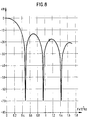
- the converter transfer function module digital analog 5 is shown in figure 8.
- the converter of the invention thus produces an attenuation 6dB instead of approximately 20 dB in the absence of a modulator.
Landscapes
- Engineering & Computer Science (AREA)
- Theoretical Computer Science (AREA)
- Compression, Expansion, Code Conversion, And Decoders (AREA)
- Analogue/Digital Conversion (AREA)
- Stabilization Of Oscillater, Synchronisation, Frequency Synthesizers (AREA)
- Amplifiers (AREA)
- Channel Selection Circuits, Automatic Tuning Circuits (AREA)
Claims (11)
- Analog-Digital-Wandler, der ein analoges Eingangssignal (x(t)) empfängt, um ein digitales Abweichungssignal (y(t)) zu erzeugen, umfassend einen Subtrahierer (1) zum Bilden der Differenz des Eingangssignals und eines Referenzsignals (Ur(t)), eine Umwandlungskette (2, 3, 4) zum Erzeugen des Abweichungssignals aus dieser Differenz und eine Rückkopplungsschleife zum Erzeugen des Referenzsignals mit Hilfe eines Digital-Analog-Wandlers (5), der ein Vergleichssignal (Uc(t)) in Reaktion auf das Abweichungssignal abgibt, dadurch gekennzeichnet, daß, wobei dem Eingangssignal (x(t)) eine Mittenfrequenz (f0) zugewiesen ist, die Rückkopplungsschleife ein Verschiebungsorgan (7) zum Verschieben der Frequenzantwort des Digital-Analog-Wandlers (5) von der Nullfrequenz zu der Mittenfrequenz (f0) umfaßt, wobei dieses Verschiebungsorgan das Referenzsignal (Ur(t)) aus dem Vergleichssignal (Uc(t)) erzeugt.
- Analog-Digital-Wandler nach Anspruch 1, dadurch gekennzeichnet, daß das Verschiebungsorgan ein Modulator (7) ist, der das Referenzsignal (Ur(t)) durch Modulation des Vergleichssignals (Uc(t)) mit Hilfe eines modulierenden Signals (md(t)) erzeugt.
- Analog-Digital-Wandler nach Anspruch 2, dadurch gekennzeichnet, daß das modulierende Signal (md(t)) eine Spektralkomponente bei einer Modulationsfrequenz (fm) gleich der Mittenfrequenz (f0) aufweist.
- Analog-Digital-Wandler nach Anspruch 2, dadurch gekennzeichnet, daß das Referenzsignal (Ur(t)) das Produkt des Vergleichssignals (Uc(t)) und des modulierenden Signals (md(t)) ist.
- Analog-Digital-Wandler nach Anspruch 4, dadurch gekennzeichnet, daß die Umslandlungskette einen Abtaster (3) umfaßt, der bei einer Abtastfrequenz (fe) arbeitet, derart, daß das Abweichungssignal (y(t)) während einer Abtastperiode (Te) einen konstanten Wert beibehält.
- Analog-Digital-Wandler nach Anspruch 5, dadurch gekennzeichnet, daß das modulierende Signal (md(t)) eine Spektralkomponente bei einer Modulationsfrequenz (fm) gleich einem Mehrfachen der Hälfte dieser Abtastfrequenz (fe) aufweist.
- Analog-Digital-Wandler nach Anspruch 5, dadurch gekennzeichnet, daß das modulierende Signal (md(t)) einen positiven Wert am Ende jeder der Abtastperioden hat.
- Analog-Digital-Wandler nach Anspruch 5, dadurch gekennzeichnet, daß die Umwandlungskette einen auf die Mittenfrequenz (f0) zentrierten Bandpaßfilter (2) umfaßt.
- Analog-Digital-Wandler nach Anspruch 5, dadurch gekennzeichnet, daß die Umwandlungskette einen Zuordner (4) umfaßt.
- Analog-Digital-Wandler nach Anspruch 9, dadurch gekennzeichnet, daß der Zuordner (4) ein Komparator ist.
- Analog-Digital-Wandler nach einem der vorhergehenden Ansprüche, dadurch gekennzeichnet, daß er einen Tiefpaßfilter (6) umfaßt, der zwischen dem Digital-Analog-Wandler (5) und dem Verschiebungsorgan (7) angeordnet ist.
Applications Claiming Priority (2)
| Application Number | Priority Date | Filing Date | Title |
|---|---|---|---|
| FR9308625A FR2707815B1 (fr) | 1993-07-13 | 1993-07-13 | Convertisseur analogique numérique à boucle de contre-réaction modulée. |
| FR9308625 | 1993-07-13 |
Publications (2)
| Publication Number | Publication Date |
|---|---|
| EP0635946A1 EP0635946A1 (de) | 1995-01-25 |
| EP0635946B1 true EP0635946B1 (de) | 1998-09-30 |
Family
ID=9449225
Family Applications (1)
| Application Number | Title | Priority Date | Filing Date |
|---|---|---|---|
| EP94401587A Expired - Lifetime EP0635946B1 (de) | 1993-07-13 | 1994-07-08 | AD-Wandler mit modulierten Rückkopplungsschleife |
Country Status (8)
| Country | Link |
|---|---|
| US (1) | US5565868A (de) |
| EP (1) | EP0635946B1 (de) |
| JP (1) | JP3212222B2 (de) |
| AT (1) | ATE171828T1 (de) |
| DE (1) | DE69413617T2 (de) |
| ES (1) | ES2124860T3 (de) |
| FI (1) | FI943289L (de) |
| FR (1) | FR2707815B1 (de) |
Families Citing this family (12)
| Publication number | Priority date | Publication date | Assignee | Title |
|---|---|---|---|---|
| JP3310114B2 (ja) * | 1994-09-14 | 2002-07-29 | 株式会社東芝 | 周波数変換機能を有するa/d変換装置およびこれを用いた無線機 |
| US7218448B1 (en) * | 1997-03-17 | 2007-05-15 | The Regents Of The University Of Colorado | Extended depth of field optical systems |
| DE19701844A1 (de) * | 1997-01-21 | 1998-07-23 | Motorola Inc | Filter zur Störsignalunterdrückung |
| US6121910A (en) * | 1998-07-17 | 2000-09-19 | The Trustees Of Columbia University In The City Of New York | Frequency translating sigma-delta modulator |
| JP3504158B2 (ja) | 1998-09-29 | 2004-03-08 | 株式会社東芝 | 周波数変換機能を有するa/d変換装置及びこれを用いた無線機 |
| US7072412B1 (en) | 1999-11-09 | 2006-07-04 | Maurice Bellanger | Multicarrier digital transmission system using an OQAM transmultiplexer |
| EP1384314B1 (de) * | 2001-05-01 | 2012-01-25 | Panasonic Corporation of North America | Frequenzumsetzer unter verwendung von unterabtastung |
| US6611222B1 (en) | 2002-06-03 | 2003-08-26 | Charles Douglas Murphy | Low-complexity high-speed analog-to-digital converters |
| DE102006023697B4 (de) * | 2006-05-19 | 2008-02-07 | Infineon Technologies Ag | Verfahren zum Decodieren, Decodierer, Codierer-Decodierer-System und Wandler |
| RU2734129C2 (ru) | 2015-12-10 | 2020-10-13 | Конинклейке Филипс Н.В. | Зонд системы ультразвуковой визуализации, и система, и способ визуализации |
| US11894864B2 (en) * | 2022-03-23 | 2024-02-06 | Silicon Laboratories Inc. | Analog-to-digital converter having punctured quantizer |
| US12512852B2 (en) | 2023-08-23 | 2025-12-30 | Silicon Laboratories Inc. | Noise-shaping converter with digital modulator |
Family Cites Families (6)
| Publication number | Priority date | Publication date | Assignee | Title |
|---|---|---|---|---|
| DE2849001C2 (de) * | 1978-11-11 | 1982-10-07 | TE KA DE Felten & Guilleaume Fernmeldeanlagen GmbH, 8500 Nürnberg | Netzwerk für adaptive Deltamodulation |
| US5039909A (en) * | 1989-04-24 | 1991-08-13 | U.S. Philips Corporation | Electric lamp and holder for such a lamp |
| EP0399738A3 (de) * | 1989-05-26 | 1991-05-08 | Gec-Marconi Limited | Analog-/Digitalwandler |
| JP3048263B2 (ja) * | 1991-09-02 | 2000-06-05 | 株式会社日立製作所 | アナログ/ディジタル変換器 |
| US5351048A (en) * | 1992-04-09 | 1994-09-27 | Yoshio Yamasaki | One bit high speed signal processing system utilizing controlled spectrum of quantization noise |
| US5257026A (en) * | 1992-04-17 | 1993-10-26 | Crystal Semiconductor, Inc. | Method and apparatus for calibrating a multi-bit delta-sigma modular |
-
1993
- 1993-07-13 FR FR9308625A patent/FR2707815B1/fr not_active Expired - Fee Related
-
1994
- 1994-07-08 DE DE69413617T patent/DE69413617T2/de not_active Expired - Fee Related
- 1994-07-08 ES ES94401587T patent/ES2124860T3/es not_active Expired - Lifetime
- 1994-07-08 AT AT94401587T patent/ATE171828T1/de not_active IP Right Cessation
- 1994-07-08 EP EP94401587A patent/EP0635946B1/de not_active Expired - Lifetime
- 1994-07-11 FI FI943289A patent/FI943289L/fi unknown
- 1994-07-12 US US08/273,802 patent/US5565868A/en not_active Expired - Fee Related
- 1994-07-13 JP JP16158794A patent/JP3212222B2/ja not_active Expired - Fee Related
Also Published As
| Publication number | Publication date |
|---|---|
| FI943289A7 (fi) | 1995-01-14 |
| JP3212222B2 (ja) | 2001-09-25 |
| DE69413617D1 (de) | 1998-11-05 |
| FR2707815B1 (fr) | 1995-08-25 |
| FI943289L (fi) | 1995-01-14 |
| FI943289A0 (fi) | 1994-07-11 |
| DE69413617T2 (de) | 1999-03-11 |
| JPH07170189A (ja) | 1995-07-04 |
| FR2707815A1 (fr) | 1995-01-20 |
| EP0635946A1 (de) | 1995-01-25 |
| ATE171828T1 (de) | 1998-10-15 |
| ES2124860T3 (es) | 1999-02-16 |
| US5565868A (en) | 1996-10-15 |
Similar Documents
| Publication | Publication Date | Title |
|---|---|---|
| EP0635946B1 (de) | AD-Wandler mit modulierten Rückkopplungsschleife | |
| EP1646147B1 (de) | Analoges Filter für zeitdiskrete Signale aus passiven Bauelementen | |
| FR2702902A1 (fr) | Récepteur numérique à fréquence intermédiaire et procédé de filtrage en bande de base mis en Óoeuvre dans ce récepteur. | |
| EP2360839A1 (de) | Zeitkontinuierlicher Analog-Digital-Wandler | |
| GB2233518A (en) | Analogue to digital converters | |
| FR2743960A1 (fr) | Convertisseur numerique analogique a haute resolution destine notamment a l'accord d'un oscillateur a quartz controle par tension | |
| EP3053274B1 (de) | Zeitkontinuierliche quantisierungsvorrichtung, funkfrequenzsignalempfänger mit einer derartigen vorrichtung und zeitkontinuierliches quantisierungsverfahren | |
| FR2826207A1 (fr) | Convertisseur analogique-numerique sigma-delta passe-bande et convertisseur sigma-delta mash l'incorporant | |
| FR2618960A1 (fr) | Filtre de gammes de frequences adaptatif non lineaire a faible dephasage | |
| EP1514352B1 (de) | Verzögerungsverriegelter kreis | |
| EP0246135B1 (de) | Phasen- und Frequenzdetektor und seine Anwendung in einer Phasenregelschleife | |
| EP3048730B1 (de) | Vorrichtung zur erzeugung einer rückkopplungsschleifenfrequenz | |
| FR2805683A1 (fr) | Procede et dispositif pour la conversion analogique/numerique d'un signal | |
| EP1077530B1 (de) | Verfahren und Anordnung zur Wandlung eines Analogsignals in einem Digitalsignal mit automatischer Verstärkungsregelung | |
| FR2502872A1 (fr) | Organe de recuperation de porteuse pour signal a modulations mdp2 ou mdp4 | |
| EP1156586B1 (de) | Analog-Digital-Wandler nach dem Fliessbandverfahren mit Rauschformung | |
| EP2383892B1 (de) | Quantifizierungsvorrichtung, Funksignalempfänger, der eine solche Vorrichtung umfasst, und Quantifizierungsverfahren | |
| EP2342829A1 (de) | Verfahren zur schleifenverzögerungssteuerung bei einem sigma-delta-modulator und sigma-delta-modulator mit diesem verfahren | |
| EP4333313B1 (de) | Mehrkanalsende- und/oder empfangssystem mit mindestens n parallelen verarbeitungspfaden und verfahren zur dekorrelation von quantisierungsrauschen in einem solchen system | |
| EP1014637A1 (de) | Direktmischempfänger für FSK-modulierte Signale | |
| EP0068938A1 (de) | Logischer Erzeuger von periodischen Signalen | |
| FR2999836A1 (fr) | Procede de conversion numerique analogique a modulation de largeur d'implulsion optimise | |
| FR2864734A1 (fr) | Modulateur sigma-delta numerique simple boucle d'ordre eleve | |
| WO2002005450A1 (fr) | Procede de reception d'un signal transmis par l'intermediaire du reseau electrique et dispositif pour sa mise en oeuvre | |
| FR2907987A1 (fr) | Dispositif de boucle fermee d'asservissement et modulateur sigma-delta |
Legal Events
| Date | Code | Title | Description |
|---|---|---|---|
| PUAI | Public reference made under article 153(3) epc to a published international application that has entered the european phase |
Free format text: ORIGINAL CODE: 0009012 |
|
| AK | Designated contracting states |
Kind code of ref document: A1 Designated state(s): AT BE CH DE DK ES FR GB IT LI NL SE |
|
| 17P | Request for examination filed |
Effective date: 19950616 |
|
| GRAG | Despatch of communication of intention to grant |
Free format text: ORIGINAL CODE: EPIDOS AGRA |
|
| 17Q | First examination report despatched |
Effective date: 19971124 |
|
| GRAG | Despatch of communication of intention to grant |
Free format text: ORIGINAL CODE: EPIDOS AGRA |
|
| GRAH | Despatch of communication of intention to grant a patent |
Free format text: ORIGINAL CODE: EPIDOS IGRA |
|
| GRAH | Despatch of communication of intention to grant a patent |
Free format text: ORIGINAL CODE: EPIDOS IGRA |
|
| GRAA | (expected) grant |
Free format text: ORIGINAL CODE: 0009210 |
|
| RAP1 | Party data changed (applicant data changed or rights of an application transferred) |
Owner name: ALCATEL ALSTHOM COMPAGNIE GENERALE D'ELECTRICITE |
|
| AK | Designated contracting states |
Kind code of ref document: B1 Designated state(s): AT BE CH DE DK ES FR GB IT LI NL SE |
|
| PG25 | Lapsed in a contracting state [announced via postgrant information from national office to epo] |
Ref country code: NL Free format text: LAPSE BECAUSE OF FAILURE TO SUBMIT A TRANSLATION OF THE DESCRIPTION OR TO PAY THE FEE WITHIN THE PRESCRIBED TIME-LIMIT Effective date: 19980930 Ref country code: AT Free format text: LAPSE BECAUSE OF FAILURE TO SUBMIT A TRANSLATION OF THE DESCRIPTION OR TO PAY THE FEE WITHIN THE PRESCRIBED TIME-LIMIT Effective date: 19980930 |
|
| REF | Corresponds to: |
Ref document number: 171828 Country of ref document: AT Date of ref document: 19981015 Kind code of ref document: T |
|
| REG | Reference to a national code |
Ref country code: CH Ref legal event code: EP |
|
| GBT | Gb: translation of ep patent filed (gb section 77(6)(a)/1977) |
Effective date: 19981009 |
|
| REF | Corresponds to: |
Ref document number: 69413617 Country of ref document: DE Date of ref document: 19981105 |
|
| PG25 | Lapsed in a contracting state [announced via postgrant information from national office to epo] |
Ref country code: DK Free format text: LAPSE BECAUSE OF FAILURE TO SUBMIT A TRANSLATION OF THE DESCRIPTION OR TO PAY THE FEE WITHIN THE PRESCRIBED TIME-LIMIT Effective date: 19981231 |
|
| REG | Reference to a national code |
Ref country code: ES Ref legal event code: FG2A Ref document number: 2124860 Country of ref document: ES Kind code of ref document: T3 |
|
| RAP4 | Party data changed (patent owner data changed or rights of a patent transferred) |
Owner name: ALCATEL |
|
| NLV1 | Nl: lapsed or annulled due to failure to fulfill the requirements of art. 29p and 29m of the patents act | ||
| RAP4 | Party data changed (patent owner data changed or rights of a patent transferred) |
Owner name: ALCATEL |
|
| PG25 | Lapsed in a contracting state [announced via postgrant information from national office to epo] |
Ref country code: LI Free format text: LAPSE BECAUSE OF NON-PAYMENT OF DUE FEES Effective date: 19990731 Ref country code: CH Free format text: LAPSE BECAUSE OF NON-PAYMENT OF DUE FEES Effective date: 19990731 Ref country code: BE Free format text: LAPSE BECAUSE OF NON-PAYMENT OF DUE FEES Effective date: 19990731 |
|
| PLBE | No opposition filed within time limit |
Free format text: ORIGINAL CODE: 0009261 |
|
| STAA | Information on the status of an ep patent application or granted ep patent |
Free format text: STATUS: NO OPPOSITION FILED WITHIN TIME LIMIT |
|
| 26N | No opposition filed | ||
| REG | Reference to a national code |
Ref country code: FR Ref legal event code: CD |
|
| BERE | Be: lapsed |
Owner name: ALCATEL ALSTHOM CIE GENERALE D'ELECTRICITE Effective date: 19990731 |
|
| REG | Reference to a national code |
Ref country code: CH Ref legal event code: PL |
|
| PGFP | Annual fee paid to national office [announced via postgrant information from national office to epo] |
Ref country code: SE Payment date: 20010702 Year of fee payment: 8 |
|
| REG | Reference to a national code |
Ref country code: GB Ref legal event code: IF02 |
|
| PG25 | Lapsed in a contracting state [announced via postgrant information from national office to epo] |
Ref country code: SE Free format text: LAPSE BECAUSE OF NON-PAYMENT OF DUE FEES Effective date: 20020709 |
|
| EUG | Se: european patent has lapsed | ||
| PGFP | Annual fee paid to national office [announced via postgrant information from national office to epo] |
Ref country code: ES Payment date: 20030717 Year of fee payment: 10 |
|
| PGFP | Annual fee paid to national office [announced via postgrant information from national office to epo] |
Ref country code: GB Payment date: 20040618 Year of fee payment: 11 |
|
| PGFP | Annual fee paid to national office [announced via postgrant information from national office to epo] |
Ref country code: FR Payment date: 20040623 Year of fee payment: 11 |
|
| PG25 | Lapsed in a contracting state [announced via postgrant information from national office to epo] |
Ref country code: ES Free format text: LAPSE BECAUSE OF NON-PAYMENT OF DUE FEES Effective date: 20040709 |
|
| PGFP | Annual fee paid to national office [announced via postgrant information from national office to epo] |
Ref country code: DE Payment date: 20040715 Year of fee payment: 11 |
|
| PG25 | Lapsed in a contracting state [announced via postgrant information from national office to epo] |
Ref country code: IT Free format text: LAPSE BECAUSE OF NON-PAYMENT OF DUE FEES Effective date: 20050708 Ref country code: GB Free format text: LAPSE BECAUSE OF NON-PAYMENT OF DUE FEES Effective date: 20050708 |
|
| REG | Reference to a national code |
Ref country code: ES Ref legal event code: FD2A Effective date: 20040709 |
|
| PG25 | Lapsed in a contracting state [announced via postgrant information from national office to epo] |
Ref country code: DE Free format text: LAPSE BECAUSE OF NON-PAYMENT OF DUE FEES Effective date: 20060201 |
|
| GBPC | Gb: european patent ceased through non-payment of renewal fee |
Effective date: 20050708 |
|
| PG25 | Lapsed in a contracting state [announced via postgrant information from national office to epo] |
Ref country code: FR Free format text: LAPSE BECAUSE OF NON-PAYMENT OF DUE FEES Effective date: 20060331 |
|
| REG | Reference to a national code |
Ref country code: FR Ref legal event code: ST Effective date: 20060331 |