EP1014637A1 - Direktmischempfänger für FSK-modulierte Signale - Google Patents
Direktmischempfänger für FSK-modulierte Signale Download PDFInfo
- Publication number
- EP1014637A1 EP1014637A1 EP98124582A EP98124582A EP1014637A1 EP 1014637 A1 EP1014637 A1 EP 1014637A1 EP 98124582 A EP98124582 A EP 98124582A EP 98124582 A EP98124582 A EP 98124582A EP 1014637 A1 EP1014637 A1 EP 1014637A1
- Authority
- EP
- European Patent Office
- Prior art keywords
- signal
- signals
- receiver
- frequency
- amplifier
- Prior art date
- Legal status (The legal status is an assumption and is not a legal conclusion. Google has not performed a legal analysis and makes no representation as to the accuracy of the status listed.)
- Granted
Links
- 238000006243 chemical reaction Methods 0.000 title claims abstract description 21
- 230000004044 response Effects 0.000 claims abstract description 24
- 238000010606 normalization Methods 0.000 claims description 8
- 238000007493 shaping process Methods 0.000 claims description 6
- 235000008694 Humulus lupulus Nutrition 0.000 claims description 4
- 230000006870 function Effects 0.000 description 10
- 238000010586 diagram Methods 0.000 description 9
- 230000008901 benefit Effects 0.000 description 5
- 239000004065 semiconductor Substances 0.000 description 4
- 230000008859 change Effects 0.000 description 3
- 230000004048 modification Effects 0.000 description 3
- 238000012986 modification Methods 0.000 description 3
- 238000005516 engineering process Methods 0.000 description 2
- 238000004519 manufacturing process Methods 0.000 description 2
- 230000002123 temporal effect Effects 0.000 description 2
- 230000006872 improvement Effects 0.000 description 1
- 230000007704 transition Effects 0.000 description 1
Images


Classifications
-
- H—ELECTRICITY
- H04—ELECTRIC COMMUNICATION TECHNIQUE
- H04L—TRANSMISSION OF DIGITAL INFORMATION, e.g. TELEGRAPHIC COMMUNICATION
- H04L27/00—Modulated-carrier systems
- H04L27/10—Frequency-modulated carrier systems, i.e. using frequency-shift keying
- H04L27/14—Demodulator circuits; Receiver circuits
- H04L27/144—Demodulator circuits; Receiver circuits with demodulation using spectral properties of the received signal, e.g. by using frequency selective- or frequency sensitive elements
- H04L27/152—Demodulator circuits; Receiver circuits with demodulation using spectral properties of the received signal, e.g. by using frequency selective- or frequency sensitive elements using controlled oscillators, e.g. PLL arrangements
- H04L27/1525—Demodulator circuits; Receiver circuits with demodulation using spectral properties of the received signal, e.g. by using frequency selective- or frequency sensitive elements using controlled oscillators, e.g. PLL arrangements using quadrature demodulation
Definitions
- the present invention relates to the technical field of receivers capable of demodulating electrical signals and, more specifically, direct conversion receivers for frequency hopping modulated signals.
- the patent EP 0.405.676 describes a receiver 1 comprising connected in series a antenna 2, direct conversion means 3, two limiting amplifiers 28 and 30, a demodulation means 5 and a bistable memory 6.
- the antenna 2 receives a signal S modulated by frequency hopping and provides this signal.
- a modulation by frequency hopping ⁇ called ⁇ FSK modulation ⁇ (acronym from English ⁇ Frequency-Shift Keying ⁇ ) is a modulation allowing the supply of a signal at a frequency equal to a value fp + ⁇ f1 for transmit one of the two signal states, and to another value fp- ⁇ f1 for transmit the other state, the references fp and ⁇ f1 designating respectively a nominal carrier frequency and an offset frequency.
- the frequencies fp and ⁇ f1 are respectively worth 400 MHz and 4.5 kHz.
- the conversion means 3 comprises two mixers 12 and 14, one local oscillator 16, a 90 ° phase shifter and two low-pass filters 20 and 22.
- the oscillator 16 provides a frequency fL which is ideally equal to the carrier frequency fp.
- the mixer 12 (respectively 14) comprises a first input terminal to receive signal S, a second terminal input to receive the frequency fL, and an output terminal connected to the filter 20 (respectively 22).
- the mixer 14 is connected to the oscillator 16, via the phase shifter 18.
- the filter 20 can receive the frequency supplied by the mixer 12 (respectively 14) and, in response, provide a signal I (respectively a signal Q).
- FIG. 2 represents two timing diagrams 24 and 26 illustrating the signals I and Q, respectively.
- the I and Q signals are analog signals having substantially sinusoidal waveforms and in phase quadrature.
- the presence of a phase change in the signal Q as illustrated in timing diagram 26.
- the limiting amplifiers 28 and 30 can receive I and Q signals and, in response, provide I1 and Q1, respectively.
- a limiting amplifier receives a signal input, and provides an output signal whose amplitude does not increase practically more beyond a determined amplitude of the input signal.
- the FIG. 3A of the present description represents two timing diagrams 32 and 34 illustrating the signals I1 and Q1, respectively.
- the signals I1 and Q1 are digital signals having forms of waves offset from each other and rectangular, the amplitudes of the signals I1 and Q1 being equal to -1 or +1.
- FIG. 3B represents a curve 80 illustrating the relationship between the instantaneous values I1 (t) and Q1 (t) of the signals I1 and Q1 at an instant t.
- the curve 80 has a rectangular shape whose vertices are formed by four points A to D. It is noted that a temporal evolution of these signals results in a course along this curve, so that, when the signal Vout is worth 0 (respectively 1), the signals I1 and Q1 are represented successively by the points A, B, C, D, A ... (respectively A, D, C, B, A ...), that is to say a course according to the direction trigonometric (respectively in the opposite direction to the direction trigonometric).
- the demodulation means 5 comprises connected in series a differentiator circuit 40 (respectively 42), a multiplier 36 (respectively 38) and a subtractor 39.
- the multiplier 36 (respectively 38) comprises a first terminal input to receive signal Q1 (respectively I1), and a second input terminal to receive the signal I1 (respectively Q1), by through the differentiating circuit 40 (respectively 42).
- the multiplier 36 (respectively 38) is arranged to supply the signal X1 (respectively Y1).
- Figure 4 of this description shows two timing diagrams 44 and 46 illustrating the signals X1 and Y1, respectively. As shown in Figure 4, the signal X1 contains first pulses, and signal Y1 contains second pulses offset by compared to the first pulses.
- Subtractor 39 includes a first input terminal to receive signal X1 and a second terminal input to receive signal Y1.
- the subtractor 39 is arranged for provide a signal X1-Y1 equal to the difference between the signals X1 and Y1.
- the Figure 5 of this description shows a timing diagram 48 illustrating the signal X1-Y1.
- the signal X1-Y1 contains the pulses resulting from the difference between signals X1 and Y1.
- signal X1-Y1 contains negative pulses and that this phase change causes the supply of positive impulses.
- the bistable memory 6 includes an input terminal for receiving the signal X1-Y1, and an output terminal to provide a Vout signal in response.
- Figure 6 of this description shows a timing diagram 50 illustrating the signal Vout.
- the signal Vout is equal to a level ⁇ 0 ⁇ or a level ⁇ 1 ⁇ .
- the signal Vout switches from level ⁇ 0 ⁇ at level ⁇ 1 ⁇ , and remains at this level, regardless of subsequent difference in frequencies between signals X1 and Y1.
- the signals I1 and Q1 are periodical T, the signal I1 being ahead of the signal Q1, so that the signal Vout is worth 0.
- the signals I1 and Q1 are represented successively by the points A, B, C, D, A ...
- the signal Q1 becomes equal to 1.
- a new information is present in the Q signal, so the timing of signals I1 and Q1 is reversed beyond time t01 + T / 2 (i.e. the signals I1 and Q1 are represented successively by points B, A, D, C, B ).
- the patent US 5,640,428 describes a receiver 90 comprising an antenna 2, a means conversion 3, a demodulation means 92 and a low-pass filter 94.
- the demodulation means 92 comprises four mixers 96 to 99, two holding circuits 100 and 101 and three delay circuits 102 to 104.
- the receiver 90 performs a demodulation of a signal S received by antenna 2, by analog processing of this signal. However this processing is carried out by digital processing elements (signals clock, flip-flops), like receiver 1 in Figure 1.
- receivers 1 and 90 contain multipliers which are components with a complex structure (in particular two terminals input) i.e. components that are difficult to manufacture.
- An object of the present invention is to provide a receiver for FSK modulated signals overcoming the aforementioned drawbacks, in particular a such receiver performing instant demodulation on the basis of signals analog.
- Another object of the present invention is to provide a receiver for FSK modulated signals demodulating information received with a minimum ⁇ f / D ratio (typically less than 1).
- Another object of the present invention is to provide a receiver for FSK modulated signals comprising a demodulation means devoid of multipliers.
- Another object of the present invention is to provide a receiver for FSK modulated signals meeting the criteria of rationality, congestion and cost, which are traditional in the semiconductor industry.
- An advantage of the complex filter of such a receiver is that it can be made of semiconductor components that are simple to manufacture, without train multipliers or mixers with several inputs, like conventional receivers.
- Another advantage of the filter of such a receiver is to filter half of the noise from the modulated signal, which significantly reduces the influence of noise on the receiver output signal.
- FIG. 8 represents a receiver 110 according to the present invention comprising an antenna 2, a conversion means 3, a means of demodulation 112 and a formatting means 114.
- the demodulation means 112 comprises a complex filter 116, two normalization means 118 and 120 and a summator 122.
- the complex filter 116 is arranged to receive the analog signals I and Q supplied by the conversion means 3, as has already been described in more detail with reference to FIG. 1.
- the complex filter 116 is also arranged so that the values of the gain
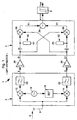
- FIG. 9 represents an embodiment of the complex filter 116 comprising two summers 124 and 126, six amplifiers 128, 130, 132, 134, 136 and 138, and two integrators 140 and 142.
- the gains of amplifiers 128 and 130 are worth fo, than those of amplifiers 132 and 134 are equal to -1 and those of amplifiers 136 and 138 are equal to -fc / fo.
- the summator 124, the integrator 140 and the amplifier 128 are connected in series, and arranged so that the adder 124 receives the signal analog I and that the amplifier 128 provides the signal X3.
- the summator 124 also receives the signal X3 via the amplifier 132.
- the summator 126, the integrator 142 and the amplifier 130 are connected in series, and arranged so that the summator 126 receives the signal analog Q and that the amplifier 130 supplies the signal Y3.
- the summator 126 also receives the signal Y3 via the amplifier 134.
- the summator 124 also receives the signal Y3 via the amplifier 136, and the summator 126 also receives the signal X3 by through amplifier 138.
- the conversion means 3 and the means of demodulation 112 by forming components (achievable by a CMOS type technology), so that the amplitudes of the X3 and Y3 signals are equal.
- the receiver 110 can include two variable gain amplifiers (known per se) connected so that the conversion means 3 supplies the signal I with demodulation 112 (respectively signal Q), via one of these amplifiers (respectively from the other of these amplifiers).
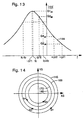
- FIG. 10 represents a curve 144 illustrating the gain
- the filter 116 can be considered as a bandpass filter whose cutoff frequencies are equal to fc-fo and fc + fo.
- Figure 11 illustrates the relationship between the instantaneous values X3 (t) and Y3 (t) of signals X3 and Y3 at an instant t.
- the instantaneous values X3 (t) and Y3 (t) describe a first circle or circle 145 and a second circle or circle 146.
- the radius of the circle 146 is worth + G2 and the radius of circle 145 is + G1.
- the normalization means 118 is arranged to receive the analog signal X3 and, in response, provide a signal representing a standard of the signal X3.
- the conversion means 118 is produced by semiconductor components (achievable in CMOS type technology) so that this standard corresponds to the square function.
- the reference X3 2 designates the signal representing this standard of the signal X3.
- the normalization means 120 is arranged to receive the analog signal Y3 and, in response, to supply a signal representing the same standard of the signal Y3.
- the conversion means 118 is produced by semiconductor components so that this standard corresponds to the square function.
- the reference Y3 2 designates the signal representing this standard of the signal Y3.
- the adder 122 is arranged to receive the signals X3 2 and Y3 2 and, in response, to provide a signal X3 2 + Y3 2 representing the sum of the signals X3 2 and Y3 2 . It is noted that the signal X3 2 + Y3 2 is an analog signal.
- the shaping means 114 is arranged to receive the analog signal X3 2 + Y3 2 and, in response, provide a digital signal Vo equal to a level ⁇ 0 ⁇ (respectively a level ⁇ 1 ⁇ ), when the signal X3 2 + Y3 2 is lower (respectively higher) than a predetermined threshold.
- the shaping means 114 are preferably produced by forming a threshold comparator, this threshold corresponding to the predetermined threshold and being chosen to be between the values + G1 2 and + G2 2 .
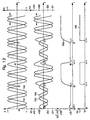
- FIG. 12 represents six chronograms 151 to 156.
- the conversion means 3 supplies the signals I and Q so that these signals have sinusoidal waveforms of period T (corresponding to the frequency + ⁇ f1) and in phase quadrature, the signal Q being in advance. on signal I.
- the maximum and minimum amplitudes of the signals I and Q are equal to 1.
- is worth + G2, as has already been described in relation to FIG. 10. It follows that, beyond the instant t0, the values X3 (t) and Y3 (t) of the signals X3 and Y3 describe the circle 146, that is to say that the signals X3 and Y3 have sinusoidal waveforms at the frequency + ⁇ f1 and in phase quadrature, the signal Y3 being ahead of the signal X3.
- the signals X3 and Y3 are proportional to the respective signals I and Q, but behind by a period T1 with respect to the latter, and that they have minimum and maximum amplitudes equal to + G2 and -G2, respectively .
- the normalization means 118 and 120 respectively supply the signals X3 2 and Y3 2 to the summator 122, and the latter supplies in response the signal X3 2 + Y3 2 equal, in this case, to + G2 2 .
- the shaping means 114 supplies in response the signal Vo equal to the level ⁇ 0 ⁇ .
- the complex filter 116 supplies the signals X3 and Y3 so that the gain
- the signals X3 and Y3 are proportional to the signals I and Q, respectively, and have minimum and maximum amplitudes equal to + G1 and -G1.
- the normalization means 118 and 120 respectively supply the signals X3 2 and Y3 2 to the summator 122, and the latter supplies in response the signal X3 2 + Y3 2 equal, in this case, to + G1 2 .
- the shaping means 114 supplies in response the signal Vo equal to the level ⁇ 1 ⁇ .
- the transition between the levels ⁇ 0 ⁇ and ⁇ 1 ⁇ takes place by continuous variations of the signals X3 and Y3 at time t7, as shown in Figure 11.
- the antenna 2 receives a signal at frequency fp + ⁇ f1.
- the situation is similar to that described for time t0. It follows that, beyond the instant t5, the means of setting in form 114 provides in response the signal Vo equal to the level ⁇ 0 ⁇ .
- the antenna 2 receives a signal at frequency fp- ⁇ f1.
- the situation is similar to that described for time t5. It follows that, beyond the instant t7, the means of setting form 114 provides in response the signal Vo equal to the level ⁇ 1 ⁇ .
- the delay T1 between the time when the information is provided by the conversion means 3 and the time when the information is contained in the signal Vo is essentially due to the response time of the complex filter 116, that is to say the response time of the integrators 140 and 142 of this filter.
- This is particularly advantageous, since several pieces of information can thus be received by the antenna 2 and supplied in the form of signal Vo, during the same half-cycle (for example at times t6 and t7).
- the receiver 110 can operate with a low ratio ⁇ f / D (in this example, less than 1), which allows the supply of at least four bits during a period of the signal Vo.
- H3 (jf) an advantage of the transfer function H3 (jf) is to allow a demodulation of the signals I and Q, from an amplitude relation linked to the gain
- receiver 110 can demodulate FSK modulated signals with N frequency jumps designated ⁇ f 1 , ⁇ f 2 , ... ⁇ f N , without structural modification of this receiver (with the exception of the setting means form 114 produced, in this case, by a comparator with N-1 thresholds).
- the values X3 (t) and Y3 (t) can describe a third circle or circle 169 and a fourth circle or circle 170. It is noted that, in the case where the maximum (respectively minimum) amplitudes of the signals I and Q are worth 1 (respectively -1), the radius of the circle 169 is worth G3 and the radius of the circle 170 is worth G4.
- the means for normalizing the receiver according to the present invention can be arranged to provide as standard the function absolue absolute value ⁇ , or function ⁇ power 2m ⁇ , the reference m being an integer greater than or equal to 2.
Landscapes
- Physics & Mathematics (AREA)
- Spectroscopy & Molecular Physics (AREA)
- Engineering & Computer Science (AREA)
- Computer Networks & Wireless Communication (AREA)
- Signal Processing (AREA)
- Digital Transmission Methods That Use Modulated Carrier Waves (AREA)
Priority Applications (4)
| Application Number | Priority Date | Filing Date | Title |
|---|---|---|---|
| DE69834407T DE69834407T2 (de) | 1998-12-23 | 1998-12-23 | Direktmischempfänger für FSK-modulierte Signale |
| EP98124582A EP1014637B1 (de) | 1998-12-23 | 1998-12-23 | Direktmischempfänger für FSK-modulierte Signale |
| US09/466,892 US6563887B1 (en) | 1998-12-23 | 1999-12-20 | Direct conversion receiver for frequency-shift keying modulated signals |
| JP36691099A JP4267786B2 (ja) | 1998-12-23 | 1999-12-24 | 周波数偏移変調信号用の直接変換受信機 |
Applications Claiming Priority (1)
| Application Number | Priority Date | Filing Date | Title |
|---|---|---|---|
| EP98124582A EP1014637B1 (de) | 1998-12-23 | 1998-12-23 | Direktmischempfänger für FSK-modulierte Signale |
Publications (2)
| Publication Number | Publication Date |
|---|---|
| EP1014637A1 true EP1014637A1 (de) | 2000-06-28 |
| EP1014637B1 EP1014637B1 (de) | 2006-05-03 |
Family
ID=8233236
Family Applications (1)
| Application Number | Title | Priority Date | Filing Date |
|---|---|---|---|
| EP98124582A Expired - Lifetime EP1014637B1 (de) | 1998-12-23 | 1998-12-23 | Direktmischempfänger für FSK-modulierte Signale |
Country Status (4)
| Country | Link |
|---|---|
| US (1) | US6563887B1 (de) |
| EP (1) | EP1014637B1 (de) |
| JP (1) | JP4267786B2 (de) |
| DE (1) | DE69834407T2 (de) |
Families Citing this family (2)
| Publication number | Priority date | Publication date | Assignee | Title |
|---|---|---|---|---|
| JP4063563B2 (ja) * | 2002-03-25 | 2008-03-19 | 株式会社日立国際電気 | 直接検波回路 |
| US7146148B2 (en) * | 2002-10-01 | 2006-12-05 | Hitachi Kokusai Electric Inc. | Low intermediate frequency type receiver |
Citations (4)
| Publication number | Priority date | Publication date | Assignee | Title |
|---|---|---|---|---|
| US4437068A (en) * | 1981-02-19 | 1984-03-13 | Thomson-Csf | FSK Demodulator for frequency-modulation modem |
| EP0305125A1 (de) * | 1987-08-21 | 1989-03-01 | BRITISH TELECOMMUNICATIONS public limited company | FSK-Diskriminator |
| EP0405676A2 (de) * | 1989-06-30 | 1991-01-02 | Philips Electronics Uk Limited | Direktmisch-FSK-Empfänger mit einer von Frequenzabweichung unabhängigen Ausgangsgleichspannung |
| US5640428A (en) * | 1994-11-10 | 1997-06-17 | Matsushita Electric Industrial Co, Ltd. | Direct conversion receiver |
Family Cites Families (6)
| Publication number | Priority date | Publication date | Assignee | Title |
|---|---|---|---|---|
| GB2149244B (en) * | 1983-10-29 | 1987-01-21 | Standard Telephones Cables Ltd | Digital demodulator arrangement for quadrature signals |
| US5249203A (en) * | 1991-02-25 | 1993-09-28 | Rockwell International Corporation | Phase and gain error control system for use in an i/q direct conversion receiver |
| US5828705A (en) * | 1996-02-01 | 1998-10-27 | Kroeger; Brian W. | Carrier tracking technique and apparatus having automatic flywheel/tracking/reacquisition control and extended signal to noise ratio |
| US5937341A (en) * | 1996-09-13 | 1999-08-10 | University Of Washington | Simplified high frequency tuner and tuning method |
| EP0948128B1 (de) * | 1998-04-03 | 2004-12-01 | Motorola Semiconducteurs S.A. | Unterdrückung von Gleichspannungsverschiebungen in einem Quadraturempfänger |
| US6304751B1 (en) * | 1998-12-29 | 2001-10-16 | Cirrus Logic, Inc. | Circuits, systems and methods for digital correction of phase and magnitude errors in image reject mixers |
-
1998
- 1998-12-23 EP EP98124582A patent/EP1014637B1/de not_active Expired - Lifetime
- 1998-12-23 DE DE69834407T patent/DE69834407T2/de not_active Expired - Lifetime
-
1999
- 1999-12-20 US US09/466,892 patent/US6563887B1/en not_active Expired - Lifetime
- 1999-12-24 JP JP36691099A patent/JP4267786B2/ja not_active Expired - Fee Related
Patent Citations (4)
| Publication number | Priority date | Publication date | Assignee | Title |
|---|---|---|---|---|
| US4437068A (en) * | 1981-02-19 | 1984-03-13 | Thomson-Csf | FSK Demodulator for frequency-modulation modem |
| EP0305125A1 (de) * | 1987-08-21 | 1989-03-01 | BRITISH TELECOMMUNICATIONS public limited company | FSK-Diskriminator |
| EP0405676A2 (de) * | 1989-06-30 | 1991-01-02 | Philips Electronics Uk Limited | Direktmisch-FSK-Empfänger mit einer von Frequenzabweichung unabhängigen Ausgangsgleichspannung |
| US5640428A (en) * | 1994-11-10 | 1997-06-17 | Matsushita Electric Industrial Co, Ltd. | Direct conversion receiver |
Also Published As
| Publication number | Publication date |
|---|---|
| JP4267786B2 (ja) | 2009-05-27 |
| US6563887B1 (en) | 2003-05-13 |
| DE69834407D1 (de) | 2006-06-08 |
| EP1014637B1 (de) | 2006-05-03 |
| JP2000196685A (ja) | 2000-07-14 |
| DE69834407T2 (de) | 2007-04-19 |
Similar Documents
| Publication | Publication Date | Title |
|---|---|---|
| EP0530107B1 (de) | PSK-Demodulator mit Korrektur im Basisband für Phasen- oder Frequenzfehler | |
| FR2550030A1 (fr) | Procede et dispositif pour la demodulation de la modulation de frequence | |
| FR2494059A1 (fr) | Procede et dispositif de demodulation de porteuse a acquisition rapide | |
| EP0451232B1 (de) | Kodeerfassungsverfahren und schaltung für spreizspektrumsignalempfänger | |
| EP0125979B1 (de) | Demodulator für Signale mit konstanter Umhüllung und kontinuierlicher Phase welche durch eine Binärsymbolreihe winkelmoduliert werden | |
| FR2669786A1 (fr) | Dispositif doubleur de frequence. | |
| EP0209928B1 (de) | Demodulator für frequenzmodulierte digitale Signale | |
| EP0635946B1 (de) | AD-Wandler mit modulierten Rückkopplungsschleife | |
| FR2551279A1 (fr) | Generateur d'onde sinusoidale, dont la frequence est asservie a un signal binaire, notamment pour modem | |
| EP1014637B1 (de) | Direktmischempfänger für FSK-modulierte Signale | |
| FR2646745A1 (fr) | Dispositif de demodulation d'un signal demodule en phase ou en frequence | |
| EP3116182B1 (de) | Quadratur-demodulator für rfid-empfänger mit sehr hohem durchsatz | |
| EP0092474B1 (de) | Demodulationsfilter für binär frequenzmoduliertes Signal | |
| EP0031762A2 (de) | Modulator-Demodulator zur Übertragung durch eine vierpegelige doppelte Amplitudenmodulation auf Quadraturträgern | |
| EP0246135B1 (de) | Phasen- und Frequenzdetektor und seine Anwendung in einer Phasenregelschleife | |
| EP0021943B1 (de) | Digitales Hyperfrequenz-Datenübertragungssystem | |
| FR2595895A1 (fr) | Double demodulateur numerique | |
| EP1514352A1 (de) | Verzögerungsverriegelter kreis | |
| RU2852743C1 (ru) | Способ фазовой манипуляции и устройство, его реализующее | |
| FR2700228A1 (fr) | Dispositif de calage de phase de chacun des paquets d'un signal numérique à modulation de phase, et récepteur correspondant. | |
| EP1089427A1 (de) | Verfarhen zum Vergleichen der Amplituden von zwei elektrischen Signalen | |
| FR3147474A1 (fr) | Décalage fréquentiel d'un signal d'horloge | |
| FR2717971A1 (fr) | Dispositif de synthèse d'une forme de signal, poste émetteur et poste récepteur comprenant un tel dispositif. | |
| WO2018115139A2 (fr) | Dispositif de génération d'un signal numérique modulé et système de génération d'un signal analogique modulé | |
| EP0068938A1 (de) | Logischer Erzeuger von periodischen Signalen |
Legal Events
| Date | Code | Title | Description |
|---|---|---|---|
| PUAI | Public reference made under article 153(3) epc to a published international application that has entered the european phase |
Free format text: ORIGINAL CODE: 0009012 |
|
| AK | Designated contracting states |
Kind code of ref document: A1 Designated state(s): CH DE FR GB IT LI NL |
|
| AX | Request for extension of the european patent |
Free format text: AL;LT;LV;MK;RO;SI |
|
| 17P | Request for examination filed |
Effective date: 20001228 |
|
| AKX | Designation fees paid |
Free format text: CH DE FR GB IT LI NL |
|
| GRAP | Despatch of communication of intention to grant a patent |
Free format text: ORIGINAL CODE: EPIDOSNIGR1 |
|
| GRAS | Grant fee paid |
Free format text: ORIGINAL CODE: EPIDOSNIGR3 |
|
| GRAA | (expected) grant |
Free format text: ORIGINAL CODE: 0009210 |
|
| AK | Designated contracting states |
Kind code of ref document: B1 Designated state(s): CH DE FR GB IT LI NL |
|
| PG25 | Lapsed in a contracting state [announced via postgrant information from national office to epo] |
Ref country code: IT Free format text: LAPSE BECAUSE OF FAILURE TO SUBMIT A TRANSLATION OF THE DESCRIPTION OR TO PAY THE FEE WITHIN THE PRESCRIBED TIME-LIMIT;WARNING: LAPSES OF ITALIAN PATENTS WITH EFFECTIVE DATE BEFORE 2007 MAY HAVE OCCURRED AT ANY TIME BEFORE 2007. THE CORRECT EFFECTIVE DATE MAY BE DIFFERENT FROM THE ONE RECORDED. Effective date: 20060503 |
|
| REG | Reference to a national code |
Ref country code: GB Ref legal event code: FG4D Free format text: NOT ENGLISH |
|
| REG | Reference to a national code |
Ref country code: CH Ref legal event code: EP |
|
| REF | Corresponds to: |
Ref document number: 69834407 Country of ref document: DE Date of ref document: 20060608 Kind code of ref document: P |
|
| REG | Reference to a national code |
Ref country code: CH Ref legal event code: NV Representative=s name: ICB INGENIEURS CONSEILS EN BREVETS SA |
|
| RAP2 | Party data changed (patent owner data changed or rights of a patent transferred) |
Owner name: ASULAB S.A. |
|
| GBT | Gb: translation of ep patent filed (gb section 77(6)(a)/1977) |
Effective date: 20060911 |
|
| NLT2 | Nl: modifications (of names), taken from the european patent patent bulletin |
Owner name: ASULAB S.A. Effective date: 20060906 |
|
| PLBE | No opposition filed within time limit |
Free format text: ORIGINAL CODE: 0009261 |
|
| STAA | Information on the status of an ep patent application or granted ep patent |
Free format text: STATUS: NO OPPOSITION FILED WITHIN TIME LIMIT |
|
| 26N | No opposition filed |
Effective date: 20070206 |
|
| REG | Reference to a national code |
Ref country code: CH Ref legal event code: PFA Owner name: ASULAB S.A. Free format text: ASULAB S.A.#FAUBOURG DU LAC 6#CH-2501 BIENNE (CH) -TRANSFER TO- ASULAB S.A.#RUE DES SORS 3#2074 MARIN (CH) |
|
| PGFP | Annual fee paid to national office [announced via postgrant information from national office to epo] |
Ref country code: NL Payment date: 20091127 Year of fee payment: 12 |
|
| REG | Reference to a national code |
Ref country code: NL Ref legal event code: V1 Effective date: 20110701 |
|
| PG25 | Lapsed in a contracting state [announced via postgrant information from national office to epo] |
Ref country code: NL Free format text: LAPSE BECAUSE OF NON-PAYMENT OF DUE FEES Effective date: 20110701 |
|
| PGFP | Annual fee paid to national office [announced via postgrant information from national office to epo] |
Ref country code: GB Payment date: 20131125 Year of fee payment: 16 |
|
| GBPC | Gb: european patent ceased through non-payment of renewal fee |
Effective date: 20141223 |
|
| PG25 | Lapsed in a contracting state [announced via postgrant information from national office to epo] |
Ref country code: GB Free format text: LAPSE BECAUSE OF NON-PAYMENT OF DUE FEES Effective date: 20141223 |
|
| REG | Reference to a national code |
Ref country code: FR Ref legal event code: PLFP Year of fee payment: 18 |
|
| PGFP | Annual fee paid to national office [announced via postgrant information from national office to epo] |
Ref country code: CH Payment date: 20151119 Year of fee payment: 18 Ref country code: DE Payment date: 20151119 Year of fee payment: 18 |
|
| PGFP | Annual fee paid to national office [announced via postgrant information from national office to epo] |
Ref country code: FR Payment date: 20151123 Year of fee payment: 18 |
|
| REG | Reference to a national code |
Ref country code: DE Ref legal event code: R119 Ref document number: 69834407 Country of ref document: DE |
|
| REG | Reference to a national code |
Ref country code: CH Ref legal event code: PL |
|
| REG | Reference to a national code |
Ref country code: FR Ref legal event code: ST Effective date: 20170831 |
|
| PG25 | Lapsed in a contracting state [announced via postgrant information from national office to epo] |
Ref country code: CH Free format text: LAPSE BECAUSE OF NON-PAYMENT OF DUE FEES Effective date: 20161231 Ref country code: LI Free format text: LAPSE BECAUSE OF NON-PAYMENT OF DUE FEES Effective date: 20161231 Ref country code: FR Free format text: LAPSE BECAUSE OF NON-PAYMENT OF DUE FEES Effective date: 20170102 |
|
| PG25 | Lapsed in a contracting state [announced via postgrant information from national office to epo] |
Ref country code: DE Free format text: LAPSE BECAUSE OF NON-PAYMENT OF DUE FEES Effective date: 20170701 |