EP0636896A1 - Boundary scan cell - Google Patents
Boundary scan cell Download PDFInfo
- Publication number
- EP0636896A1 EP0636896A1 EP94305137A EP94305137A EP0636896A1 EP 0636896 A1 EP0636896 A1 EP 0636896A1 EP 94305137 A EP94305137 A EP 94305137A EP 94305137 A EP94305137 A EP 94305137A EP 0636896 A1 EP0636896 A1 EP 0636896A1
- Authority
- EP
- European Patent Office
- Prior art keywords
- flop
- input
- output
- flip
- bit
- Prior art date
- Legal status (The legal status is an assumption and is not a legal conclusion. Google has not performed a legal analysis and makes no representation as to the accuracy of the status listed.)
- Withdrawn
Links
Images

Classifications
-
- G—PHYSICS
- G11—INFORMATION STORAGE
- G11C—STATIC STORES
- G11C29/00—Checking stores for correct operation ; Subsequent repair; Testing stores during standby or offline operation
-
- G—PHYSICS
- G01—MEASURING; TESTING
- G01R—MEASURING ELECTRIC VARIABLES; MEASURING MAGNETIC VARIABLES
- G01R31/00—Arrangements for testing electric properties; Arrangements for locating electric faults; Arrangements for electrical testing characterised by what is being tested not provided for elsewhere
- G01R31/28—Testing of electronic circuits, e.g. by signal tracer
- G01R31/317—Testing of digital circuits
- G01R31/3181—Functional testing
- G01R31/3185—Reconfiguring for testing, e.g. LSSD, partitioning
- G01R31/318533—Reconfiguring for testing, e.g. LSSD, partitioning using scanning techniques, e.g. LSSD, Boundary Scan, JTAG
- G01R31/318541—Scan latches or cell details
Definitions
- This invention relates to a circuit for enabling Boundary-Scan testing of an electronic device in the manner prescribed by the ANSI/IEEE 1149.1 Standard on Boundary-Scan during a testing mode, and for enabling the device to operate with reduced propagation delays during non-testing intervals.
- Boundary-Scan test technique which is now embodied in the ANSI/IEEE 1149.1 Standard on Boundary-Scan, is practiced by providing a Boundary-Scan cell, typically a single-bit shift register, at each output node (e.g., pin) of the electronic device which is coupled to an input node of another device.
- the Boundary-Scan cell is interposed between the output node and an internal logic block which drives the node, respectively.
- Each Boundary-Scan cell associated with each separate node is coupled in series with each of the other cells in a single chain (referred to as a Boundary-Scan chain) such that the output of each preceding cell is supplied to an input of the next succeeding cell in the chain.
- each Boundary-Scan cell associated with an input node has captured the bit appearing at the output node driving the input node, then the string of bits held by the chain of Boundary-Scan cells is shifted out. A comparison is then made between the string of shifted-out bits and a reference bit string representing the bits that would be obtained when the inter-device connections (i.e., the connections between the output and the input nodes of the devices) are fault-free. Any differences between the shifted-out bit string and the reference bit string are indicative of an error.
- Boundary-Scan cell when a Boundary-Scan cell is associated with an output node, the cell is interposed between the node and the internal logic of the device which drives the node.
- a multiplexer is provided within the Boundary-Scan cell to multiplex signals from the cell and the internal logic of the device.
- the multiplexer will impart a propagation delay to signals passing between the internal logic of the device and the corresponding output node during non-testing intervals. Such a propagation delay is undesirable, especially if the electronic device is to operate at high speeds. For this reason, high-speed electronic devices heretofore have not been provided with Boundary-Scan cells, thereby precluding the ability to test inter-device connections by the Boundary-Scan test technique described above.
- Boundary-Scan cell which affords reduced propagation delays to enable such a Boundary-Scan cell to be employed in a high speed electronic device to facilitate Boundary-Scan testing.
- Boundary-Scan cell interposed between an internal logic block of an electronic device, and a device node in accordance with the apparatus of Claim 1.
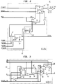
- FIG. 1 shows a portion of a digital electronic device 10 that incorporates at least one, and preferably, a plurality of conventional (prior art) Boundary-Scan cells 12 (only one shown) for facilitating testing the connections between the device 10 and one or more other devices in accordance with the Boundary-Scan test technique.
- the electronic device 10 may be comprised of a single integrated circuit, a group of circuits coupled together on a single circuit board, or even a group of circuit boards.
- the device 10 typically includes at least one, and preferably, a plurality of internal logic blocks 14 (only one shown), each having an associated Boundary-Scan cell 12. To simplify discussion, only the Boundary-Scan 12 associated with an output node will be described.
- each logic block 14 in the device 10 depends on the function(s) to be performed by the device.
- the exact details of each logic block 14 are not relevant to the Boundary-Scan cell 12, other than from the standpoint that each logic block generates a single bit output signal, hereinafter designated as FROMCKT.
- the output signal FROMCKT produced by each logic block 14 is passed to the corresponding "output" Boundary-Scan cell 12 via a system flop-flop 16, the output signal of the flip-flop being referred to as "delayed FROMCKT.”
- the system flip-flop 16 is clocked synchronously with the logic block by a common clock signal SYSCLK.
- the system flip-flop 16 has been shown separately from the internal logic block 14. In reality, the system flip-flop 16 actually comprises an integral part of the internal logic block.
- the output signal of the system flip-flop 16 (i.e., the delayed FROMCKT signal) is supplied to the Boundary-Scan cell 12 for passage therethrough, during normal operation of the device 10 (i.e., non-Boundary-Scan testing), to an output buffer 18.
- the buffer 18 drives an output node 20.
- the Boundary-Scan cell 12 is designed to be serially coupled with each of a plurality of other Boundary-Scan cells, each configured generally in the manner set forth in the aforementioned publication IEEE Standard Test Access Port and Boundary-Scan Architecture , incorporated by reference herein. The result is a single chain of cells for Boundary-Scan testing of the interconnections of the device 10 to one or more devices.
- the Boundary-Scan cell 12 includes a shift multiplexer 22 that is supplied at its first (i.e., "0") input with the output of the system flip-flop 16.
- the shift multiplexer 22 has a second (i.e., "1") input supplied with a single-bit input signal ScanIN which is received from an upstream Boundary-Scan cell (not shown) in the chain.
- the multiplexer 22 is controlled by a signal ShiftDR and, depending on that state of that signal, the multiplexer passes a separate one of the signals at its first and second inputs to a shift flip-flop 24 for receipt at its D input.
- the shift flip-flop 24 stores either the output bit of the system flip-flop 16, which indicates the state of the delayed FROMCKT signal, or stores the input bit ScanIN generated by the upstream Boundary-Scan cell in the chain.
- the shift flip-flop 24 is clocked by a clock signal ClockDR and, in response, the flip-flop generates a signal at its Q output indicative of the bit latched therein.
- the Q output signal of the shift flip-flop 24 is designated as the "ScanOUT" signal of the Boundary-Scan cell and forms a ScanIN signal supplied to a downstream Boundary-Scan cell (not shown).
- a known string of bits is shifted through the chain of Boundary-Scan cells 12 by shifting the bits through each shift register 24 of each Boundary-Scan cell in the chain.
- the signal at the Q output of the shift flip-flop 24 is also supplied to an update flip-flop 26 for receipt at its D input.
- the update flip-flop 26 is clocked by a clock signal Update DR applied to its clock input CK to latch the bit from the shift register.
- the update flip-flop 26 has its Q output coupled to one input (designated as the "1" input) of a multiplexer 28, referred to as the output multiplexer because its output is supplied to the output buffer 18.
- the output multiplexer 28 has its other input (designated the "0" input) supplied with the Q output of the system flip-flop 16.
- the multiplexer 28 passes the signal at one of its "0" and “1" inputs in accordance with the state of a single-bit signal (referred to as the "MODE" signal) applied to the multiplexer at its control input.
- the MODE signal When the MODE signal is at a first logic value (i.e., a logic "0"), designating a normal operating state for the device 10, the output multiplexer 28 passes the delayed FROMCKT signal at the output of the system flip-flop 16 to the output buffer 18. Conversely, when the MODE signal is at a second logic level (i.e., a logic "1"), indicating that the device 10 is now in a test mode, the output multiplexer 28 passes the signal from the update flip-flop 26 to the output buffer 18.
- the prior art Boundary-Scan cell 12 thus described incurs the disadvantage that the single-bit signal (i.e., the delayed FROMCKT signal), passing from the system flip-flop 16 to the output buffer 18 during normal (i.e., non-testing mode) operation of the device 10, experiences a propagation delay during passage through the output multiplexer 28.
- the propagation delay is normally measured in terms of the number of gates the bit must traverse.
- the output multiplexer 28 there are two internal gates (not shown) in the multiplexer through which the signal must pass before reaching the output buffer 18.
- the output multiplexer 28 is said to incur a two-gate delay.
- Such a delay is disadvantageous when the device 10 is to operate at high speeds.
- FIG. 2 there is shown a block schematic diagram of a Boundary-Scan cell 12', in accordance with the invention, which facilitates Boundary-Scan testing of connections of the device 10 to other such devices, yet affords a reduced propagation delay during normal (non-test mode) operation.
- the same reference numbers, each followed by a prime (') have been used in FIG. 2 to describe the corresponding elements in FIG. 1.
- the input multiplexer 22' includes a shift multiplexer 22' having a first (i.e., "0") input, and a second (i.e., "1") input, the latter being supplied with the signal ScanIN from an up-stream Boundary-Scan cell (not shown).
- the input multiplexer 22' is identical in function to the input multiplexer 22 of FIG. 1 and is thus responsive to the control signal ShiftDR. When the ShiftDR signal is at a first (i.e., "0") logic level, the input multiplexer 22' passes the signal at its "0" input to a shift flip-flop 24' for receipt at its D input.
- the multiplexer 22' passes the signal at its "1" input (i.e., the ScanIN signal) to the D input of the shift flip-flop 24'.
- the shift flip-flop 24' of FIG. 2 latches the bit received from the input multiplexer 22' so as to supply that bit to an update flip-flop 26' for receipt at its D input.
- the shift flip-flop 24' supplies its Q output signal (ScanOUT) to a downstream Boundary-Scan cell (not shown), forming that cell's ScanIN signal.
- the update flip-flop 26' of FIG. 2 operates to store the bit previously latched into the shift flip-flop 24'.
- the Boundary-Scan cell 12' of FIG. 2 differs from the cell 12 of FIG. 1 because of its lack of any output multiplexer (such as the output multiplexer 28 shown in FIG. 1). Instead, the Boundary-Scan cell 12' includes a system flip-flop 30' having asynchronous clear and preset capability.
- the system flip-flop 30' has a D input which is supplied directly with the output signal FROMCKT generated by the internal logic block 14 of FIG. 1.
- the system flip-flop 30' serves to latch the FROMCKT signal in the same way as the system-flip 16 of FIG. 1. To this extent, the system flip-flop 30' performs the same function as the system flip-flop 16.
- the Boundary-Scan cell 12' is implemented with the device 10
- the system flip-flop 16 of FIG. 1 becomes redundant and thus is deleted from the internal logic 14 of the device.
- the system flip-flop 30' has its Q output coupled to the output buffer 18. Like the system flip-flop 16 of FIG. 1, the system flip-flop 30' of FIG. 2 is clocked in response to the clock signal SYSCLK, typically the same signal clocking the internal logic block 14 of FIG. 1. Unless the system flip-flop 30' has been preset or cleared in the manner discussed below, the flip-flop supplies the output buffer 18 of the device 10 with the bit previously latched from the internal logic block 14 of FIG. 1 during the normal operating mode of the device 10. As will be described, the system flip-flop 30' performs the function of both the system flip-flop 16 of FIG. 1 and the function of the output multiplexer 28 of the Boundary-Scan cell 12 of FIG. 1. Advantageously, the system flip-flop 30' incurs 0-gate propagation delay as compared to the two-gate delay associated with the output multiplexer 28 of FIG. 1.
- the system flip-flop 30' has its QN (i.e., its Q ⁇ ) output coupled to an inverter 31' whose output is coupled to the first (i.e., "0") input of the shift multiplexer 22'.
- the shift multiplexer 22' is supplied at its first input with a signal indicative of the delayed FROMCKT signal. It may seem more efficient to simply connect the Q output of the system flip-flop 30' directly to the first input of the shift multiplexer 22', thereby avoiding the need for the inverter 31'. However, there is indeed a good reason for providing the inverter 31'.
- the system flip-flop 30' is preset and cleared asynchronously, in accordance with a preset and clear signal, respectively, applied to the flip-flop PD and CDN inputs, respectively, by a logic circuit 32' which is responsive to the MODE signal.
- the preset and clear signals which are generated by the logic circuit 32' are capable of either presetting or clearing the system flip-flop 30' without regard to the clock signal SYSCLK.
- the logic circuit 32' includes an AND gate 33' for generating the preset signal supplied to the system flip-flop 30' preset input PD in accordance with the MODE signal and with the Q output signal of the update flip-flop 26' which are received at the first and second inputs, respectively, of the AND gate.
- the logic circuit 32' also includes a NAND gate 34' which generates the clear signal CDN (which is active at a "low” logic level) supplied to the system flip-flop 30' clear input.
- the NAND gate 34' output signal is generated in accordance with the MODE signal and the QN output signal of the update flip-flop 26', which are supplied to the NAND gate at its first and second inputs, respectively.
- the AND gate 33' When the MODE signal is at a first logic level (i.e., a logic "0"), indicating that the device 10 is to operate in its normal (i.e., non-test mode), the AND gate 33' generates a logic "0" output signal and the NAND gate 34' generates a logic "1" level output signal. Under these conditions, the system flip-flop 30' is not asynchronously cleared or preset. In this way, the system flip-flop 30', when clocked by the clock signal SYSCLK, will output a bit reflecting the state of the delayed FROMCKT signal.
- the state of the MODE signal influences the preset and clear capability of the system flip-flop 30', it is important that the MODE signal be free of glitches. Even though the MODE signal is typically generated by logic circuitry separate and apart from the boundary scan cell 12', care should be taken in the design of the circuitry generating the MODE signal to avoid such glitches.
- the system flip-flop 30' advantageously passes a delayed FROMCKT signal to the output buffer 18 during non-testing intervals with a reduced propagation delay, as compared to the output multiplexer 28 of FIG. 1. This is because during non-testing intervals, the clear and the preset functions of the flip-flop are disabled. However, during testing intervals, the system flip-flop 30' operates to output a bit indicative of the bit latched in the update flip-flop 26', thus effectively passing the bit from the update flip-flop to the output buffer 18' in a fashion similar to the output multiplexer 28 of FIG. 1, but without incurring the propagation delay associated with the multiplexer.
- the system flip-flop 30' which takes the form of a positive clock-edge-triggered D flip-flop.
- the system flip-flop 30' includes a first OR gate 36' having a first input, a second input supplied with the preset signal PD, and an output which is coupled to a first input of a NAND gate 38' having a second input coupled with the clear signal CDN.
- the NAND gate 38' has its output coupled to the input of an inverter 40' whose output is coupled to a first transmission gate 42', the output of which is coupled to the first input of the OR gate 36'.
- the first input of the OR gate 36' is also coupled to the output of a second transmission gate 44' whose input forms the D input of the system flip-flop 30'.
- Each of the transmission gates 42' and 44' is responsive to a pair of control signals supplied to a separate one of a pair of control inputs c and c' on the gate. Only when each of the transmission gates 42' and 44' receives a control signal at a separate one of its c and c' inputs which is at logic "1" and logic “0" levels, respectively, will that gate pass the signal at its input to the first input of the OR gate 36'. Otherwise, no signal passes through the gate.
- the control inputs c and c' of the gates 42' and 44', respectively, are coupled to the clock input CK of the system flip-flop 36' so as to receive the SYSCLK signal applied thereto.
- the control inputs c' and c of the transmission gates 42' and 44', respectively, are each supplied with the output of an inverter 46' whose input is coupled to the clock input CK of the system flip-flop 30'.
- an inverter 46' whose input is coupled to the clock input CK of the system flip-flop 30'.
- the output of the NAND gate 38' is coupled to the input of a transmission gate 48', identical in structure to each of the transmission gates 42' and 44'.
- the transmission gate 48' has its control inputs c and c' supplied with the clock signal SYSCLK and with the output signal of the inverter 46', respectively.
- the output of the transmission gate 48' is coupled to the input of an inverter 50' whose output forms the Q output of the system flip-flop 30'.
- the QN output of the system flip-flop 30' is formed at the output of a NAND gate 52', having its first input supplied with the clear signal CDN and having a second input supplied with the output signal of an OR gate 54'.
- the OR gate 54' has a first input supplied with the preset signal PD and a second input supplied with the output of the inverter 50'.
- the output of the NAND gate 52' is supplied to the input of a transmission gate 56' having its c' and c control inputs supplied with the SYSCLK signal and its complement, respectively.
- the output of the transmission gate 56' is coupled in parallel with the output to the transmission gate 48' so as to be received at the input to the inverter 50'.
- the QN signal of the system flip-flop 30' is derived from the Q output via the gates 54' and 52'. Deriving the QN signal in this manner allows the QN signal to be complementary to the Q signal but prevents the Q output from suffering any undue loading which might adversely affect the operation of the system flip-flop 30' when the QN output drives a load.
- the flip-flop 30' operates as a conventional, positive clock-edge triggered D flip-flop.
- the output signal of the NAND gates 38' and 52' will each be at a logic "1" level, regardless of the state of the signals at the D and CK inputs of the system flip-flop 30'. Under these conditions, a logic "0" level signal will appear at the Q output of the system flip-flop 30'.
- Boundary-Scan cell 12' which enables Boundary-Scan testing of an electronic device 10, yet incurs reduced propagation for signals passing through the cell during non-testing intervals.
- Boundary-Scan cell 12' has been described in the context of being interposed between the internal logic 14 of a device 10 and a corresponding output buffer 18 which drives an output node 20, the cell, with appropriate modifications, may be employed for use with an input node, an input/output node, or a control node.
Landscapes
- Engineering & Computer Science (AREA)
- General Engineering & Computer Science (AREA)
- Physics & Mathematics (AREA)
- General Physics & Mathematics (AREA)
- Tests Of Electronic Circuits (AREA)
- Testing Or Measuring Of Semiconductors Or The Like (AREA)
Applications Claiming Priority (2)
| Application Number | Priority Date | Filing Date | Title |
|---|---|---|---|
| US08/096,286 US5490151A (en) | 1993-07-26 | 1993-07-26 | Boundary scan cell |
| US96286 | 1998-06-11 |
Publications (1)
| Publication Number | Publication Date |
|---|---|
| EP0636896A1 true EP0636896A1 (en) | 1995-02-01 |
Family
ID=22256668
Family Applications (1)
| Application Number | Title | Priority Date | Filing Date |
|---|---|---|---|
| EP94305137A Withdrawn EP0636896A1 (en) | 1993-07-26 | 1994-07-13 | Boundary scan cell |
Country Status (5)
| Country | Link |
|---|---|
| US (1) | US5490151A (ja) |
| EP (1) | EP0636896A1 (ja) |
| JP (1) | JPH07167921A (ja) |
| KR (1) | KR0169509B1 (ja) |
| TW (1) | TW487805B (ja) |
Families Citing this family (33)
| Publication number | Priority date | Publication date | Assignee | Title |
|---|---|---|---|---|
| US6304987B1 (en) * | 1995-06-07 | 2001-10-16 | Texas Instruments Incorporated | Integrated test circuit |
| DE68928613T2 (de) * | 1988-09-07 | 1998-09-24 | Texas Instruments Inc | Bidirektionale-Boundary-Scan-Testzelle |
| US5706296A (en) * | 1995-02-28 | 1998-01-06 | Texas Instruments Incorporated | Bi-directional scan design with memory and latching circuitry |
| US5969538A (en) | 1996-10-31 | 1999-10-19 | Texas Instruments Incorporated | Semiconductor wafer with interconnect between dies for testing and a process of testing |
| US5892778A (en) * | 1997-06-30 | 1999-04-06 | Sun Microsystems, Inc. | Boundary-scan circuit for use with linearized impedance control type output drivers |
| US6108807A (en) * | 1997-07-28 | 2000-08-22 | Lucent Technologies Inc. | Apparatus and method for hybrid pin control of boundary scan applications |
| US6408413B1 (en) | 1998-02-18 | 2002-06-18 | Texas Instruments Incorporated | Hierarchical access of test access ports in embedded core integrated circuits |
| US6405335B1 (en) | 1998-02-25 | 2002-06-11 | Texas Instruments Incorporated | Position independent testing of circuits |
| US5968196A (en) * | 1998-04-21 | 1999-10-19 | Atmel Corporation | Configuration control in a programmable logic device using non-volatile elements |
| US6412098B1 (en) * | 1998-06-30 | 2002-06-25 | Adaptec, Inc. | Scan cell including a propagation delay and isolation element |
| US6446230B1 (en) | 1998-09-14 | 2002-09-03 | Cisco Technology, Inc. | Mechanism for enabling compliance with the IEEE standard 1149.1 for boundary-scan designs and tests |
| US7058862B2 (en) * | 2000-05-26 | 2006-06-06 | Texas Instruments Incorporated | Selecting different 1149.1 TAP domains from update-IR state |
| US6678847B1 (en) * | 1999-04-30 | 2004-01-13 | International Business Machines Corporation | Real time function view system and method |
| US6728915B2 (en) | 2000-01-10 | 2004-04-27 | Texas Instruments Incorporated | IC with shared scan cells selectively connected in scan path |
| US6769080B2 (en) | 2000-03-09 | 2004-07-27 | Texas Instruments Incorporated | Scan circuit low power adapter with counter |
| US6567944B1 (en) * | 2000-04-25 | 2003-05-20 | Sun Microsystems, Inc. | Boundary scan cell design for high performance I/O cells |
| US6578168B1 (en) * | 2000-04-25 | 2003-06-10 | Sun Microsystems, Inc. | Method for operating a boundary scan cell design for high performance I/O cells |
| US6658632B1 (en) | 2000-06-15 | 2003-12-02 | Sun Microsystems, Inc. | Boundary scan cell architecture with complete set of operational modes for high performance integrated circuits |
| US7137052B2 (en) * | 2001-07-19 | 2006-11-14 | Verigy Ipco | Methods and apparatus for minimizing current surges during integrated circuit testing |
| US7073111B2 (en) * | 2002-06-10 | 2006-07-04 | Texas Instruments Incorporated | High speed interconnect circuit test method and apparatus |
| US20040187060A1 (en) * | 2003-03-21 | 2004-09-23 | Rohrbaugh John G. | Generating test patterns for testing an integrated circuit |
| US7389452B2 (en) * | 2004-06-29 | 2008-06-17 | Electronics For Imaging, Inc. | Methods and apparatus for monitoring internal signals in an integrated circuit |
| KR100733925B1 (ko) * | 2005-03-16 | 2007-07-02 | 주식회사 엘지화학 | ECD(Electro Chromic Device) 제어 장치 |
| US7352169B2 (en) * | 2006-05-26 | 2008-04-01 | Texas Instruments Incorporated | Testing components of I/O paths of an integrated circuit |
| US8866527B1 (en) | 2010-04-02 | 2014-10-21 | Altera Corporation | Integrated circuits with hold time avoidance circuitry |
| US8473793B2 (en) | 2010-06-10 | 2013-06-25 | Global Unichip Corporation | Low leakage boundary scan device design and implementation |
| US8539389B2 (en) | 2010-09-27 | 2013-09-17 | Teseda Corporation | Correlation of device manufacturing defect data with device electrical test data |
| US20120137187A1 (en) * | 2010-11-28 | 2012-05-31 | Freescale Semiconductor, Inc | System and method for scan testing integrated circuits |
| US8907697B2 (en) | 2011-08-31 | 2014-12-09 | Teseda Corporation | Electrical characterization for a semiconductor device pin |
| US9939488B2 (en) | 2011-08-31 | 2018-04-10 | Teseda Corporation | Field triage of EOS failures in semiconductor devices |
| US8412991B2 (en) * | 2011-09-02 | 2013-04-02 | Teseda Corporation | Scan chain fault diagnosis |
| US9599673B2 (en) | 2014-10-15 | 2017-03-21 | Freescale Semiconductor, Inc. | Structural testing of integrated circuits |
| KR20220142212A (ko) * | 2021-04-14 | 2022-10-21 | 삼성전자주식회사 | 멀티 비트 플립플롭 및 이를 포함하는 집적회로 |
Citations (3)
| Publication number | Priority date | Publication date | Assignee | Title |
|---|---|---|---|---|
| US4504784A (en) * | 1981-07-02 | 1985-03-12 | International Business Machines Corporation | Method of electrically testing a packaging structure having N interconnected integrated circuit chips |
| EP0425416A2 (en) * | 1989-10-27 | 1991-05-02 | International Business Machines Corporation | A self testable boundary logic circuit |
| EP0523438A2 (en) * | 1991-07-12 | 1993-01-20 | Motorola, Inc. | Microcomputer with boundary-scan facility |
Family Cites Families (3)
| Publication number | Priority date | Publication date | Assignee | Title |
|---|---|---|---|---|
| US5084874A (en) * | 1988-09-07 | 1992-01-28 | Texas Instruments Incorporated | Enhanced test circuit |
| US5155732A (en) * | 1990-10-09 | 1992-10-13 | At&T Bell Laboratories | Method and apparatus for data transfer to and from devices through a boundary-scan test access port |
| US5349587A (en) * | 1992-03-26 | 1994-09-20 | Northern Telecom Limited | Multiple clock rate test apparatus for testing digital systems |
-
1993
- 1993-07-26 US US08/096,286 patent/US5490151A/en not_active Expired - Lifetime
-
1994
- 1994-04-27 TW TW083103804A patent/TW487805B/zh active
- 1994-07-13 EP EP94305137A patent/EP0636896A1/en not_active Withdrawn
- 1994-07-22 JP JP6191238A patent/JPH07167921A/ja active Pending
- 1994-07-26 KR KR1019940018042A patent/KR0169509B1/ko not_active Expired - Fee Related
Patent Citations (3)
| Publication number | Priority date | Publication date | Assignee | Title |
|---|---|---|---|---|
| US4504784A (en) * | 1981-07-02 | 1985-03-12 | International Business Machines Corporation | Method of electrically testing a packaging structure having N interconnected integrated circuit chips |
| EP0425416A2 (en) * | 1989-10-27 | 1991-05-02 | International Business Machines Corporation | A self testable boundary logic circuit |
| EP0523438A2 (en) * | 1991-07-12 | 1993-01-20 | Motorola, Inc. | Microcomputer with boundary-scan facility |
Also Published As
| Publication number | Publication date |
|---|---|
| KR950004747A (ko) | 1995-02-18 |
| JPH07167921A (ja) | 1995-07-04 |
| TW487805B (en) | 2002-05-21 |
| US5490151A (en) | 1996-02-06 |
| KR0169509B1 (ko) | 1999-02-01 |
Similar Documents
| Publication | Publication Date | Title |
|---|---|---|
| US5490151A (en) | Boundary scan cell | |
| CA1218424A (en) | Scannable asynchronous/synchronous cmos latch | |
| US5602855A (en) | Integrated test circuit | |
| US5450415A (en) | Boundary scan cell circuit and boundary scan test circuit | |
| US5495487A (en) | Testing buffer/register | |
| US5056094A (en) | Delay fault testing method and apparatus | |
| KR960005606B1 (ko) | 저 대역폭 검사 장비 및 프로브 스테이션을 사용하여 디지탈 마이크로회로의 단순 및 정확한 에이씨(ac) 검사를 제공하는 내장 검사 회로 및 속도 검사 방법 | |
| EP0136461B1 (en) | Level sensitive scan design testable latch circuit apparatus | |
| US5574731A (en) | Set/reset scan flip-flops | |
| US5617426A (en) | Clocking mechanism for delay, short path and stuck-at testing | |
| US20050278133A1 (en) | Integrated test circuit | |
| US4961013A (en) | Apparatus for generation of scan control signals for initialization and diagnosis of circuitry in a computer | |
| CA2092333C (en) | Built-in self-test control network | |
| JPH0721772B2 (ja) | データ処理装置内の複数の組合せ論理素子を診断する装置 | |
| US5471152A (en) | Storage element for delay testing | |
| US5068881A (en) | Scannable register with delay test capability | |
| US5319646A (en) | Boundary-scan output cell with non-critical enable path | |
| US5831463A (en) | MOS master-slave flip-flop with reduced number of pass gates | |
| US5023875A (en) | Interlaced scan fault detection system | |
| US5793777A (en) | System and method for testing internal nodes of an integrated circuit at any predetermined machine cycle | |
| US6272656B1 (en) | Semiconductor integrated circuit including test facilitation circuit and test method thereof | |
| US5708380A (en) | Test for hold time margins in digital systems | |
| JP2785506B2 (ja) | スキャン用回路 | |
| JP2874984B2 (ja) | デジタル論理装置のスキャン回路 | |
| JPH0989993A (ja) | スキャン回路 |
Legal Events
| Date | Code | Title | Description |
|---|---|---|---|
| PUAI | Public reference made under article 153(3) epc to a published international application that has entered the european phase |
Free format text: ORIGINAL CODE: 0009012 |
|
| AK | Designated contracting states |
Kind code of ref document: A1 Designated state(s): DE ES FR GB IT |
|
| 17P | Request for examination filed |
Effective date: 19950720 |
|
| 17Q | First examination report despatched |
Effective date: 19991019 |
|
| STAA | Information on the status of an ep patent application or granted ep patent |
Free format text: STATUS: THE APPLICATION IS DEEMED TO BE WITHDRAWN |
|
| 18D | Application deemed to be withdrawn |
Effective date: 20000302 |