EP0636966A2 - Dispositif pour la conversion d'information d'affichage - Google Patents
Dispositif pour la conversion d'information d'affichage Download PDFInfo
- Publication number
- EP0636966A2 EP0636966A2 EP94305558A EP94305558A EP0636966A2 EP 0636966 A2 EP0636966 A2 EP 0636966A2 EP 94305558 A EP94305558 A EP 94305558A EP 94305558 A EP94305558 A EP 94305558A EP 0636966 A2 EP0636966 A2 EP 0636966A2
- Authority
- EP
- European Patent Office
- Prior art keywords
- data
- display
- video image
- information processing
- information
- Prior art date
- Legal status (The legal status is an assumption and is not a legal conclusion. Google has not performed a legal analysis and makes no representation as to the accuracy of the status listed.)
- Granted
Links
Images








Classifications
-
- G—PHYSICS
- G06—COMPUTING OR CALCULATING; COUNTING
- G06F—ELECTRIC DIGITAL DATA PROCESSING
- G06F3/00—Input arrangements for transferring data to be processed into a form capable of being handled by the computer; Output arrangements for transferring data from processing unit to output unit, e.g. interface arrangements
- G06F3/14—Digital output to display device ; Cooperation and interconnection of the display device with other functional units
Definitions
- the present invention relates to a display information conversion apparatus. More specifically, the present invention relates to a novel display information conversion apparatus for making a storage medium for storing a first program executed by a first information processing apparatus which is constructed so as to display an image on a dot-matrix display to be applied to a second information processing apparatus which is constructed so as to display an image on a raster-scan display, and an information processing system which utilizes such a display information conversion apparatus.
- the present invention relates to a novel display information conversion apparatus for making a storage medium for storing a first program executed by a first information processing apparatus which is constructed so as to display an image according to a first specification to be applied to a second information processing apparatus constructed so as to display an image according to a second specification in which an image quality is higher than that of the first specification.
- a dot-matrix liquid crystal game machine which has been put into a commercial market as a name of "Game Boy (trademark)", for example, is well known.
- a television game machine which has been put into a commercial market as a name of "Super Nintendo Entertainment System (trademark)", for example, is well known.
- a principal object of the present invention is to provide a novel display information conversion apparatus for making a storage medium which stores a first program capable of being executed by a first information processing apparatus which is constructed so as to display an image on a dot-matrix display to be applied to a second information processing apparatus which is constructed so as to display an image on a raster-scan display.
- Another object of the present invention is to provide an information processing system which includes the above described display information conversion apparatus.
- Another object of the present invention is to provide a novel display information conversion apparatus for making a storage medium which stores a first program capable of being executed by a first information processing apparatus which is constructed so as to display an image according to a first specification or format to be applied to a second information processing apparatus which is constructed so as to display an image according to a second specification or format in which an image quality becomes higher than that of the first specification.
- a display information conversion apparatus is an apparatus for making a storage medium which stores a first program executed by a first information processing apparatus which is constructed so as to display an image on a dot-matrix display to be applied to a second information processing apparatus which is constructed so as to display an image on a raster-scan display, and comprises: a first connection portion to which the storage medium is detachably attached; a second connection portion for detachably attaching the display information conversion apparatus to a second information processing apparatus; information processing means for executing the first program stored in the storage medium attached to the first connection portion to generate first video image information capable of being displayed on the dot-matrix display; video image converting means for converting the first video image information into second video image information capable of displayed on the raster-scan display; and transfer means for transferring the second video image information converted by the video image converting means to the second information processing apparatus via the second connection portion.
- a display information conversion apparatus is an apparatus for making a storage medium which stores in a non-volatile manner a first program capable of being executed by a first information processing apparatus which is constructed so as to display an image according to a first specification or format to be applied to a second information processing apparatus which is constructed so as to display an image according to a second specification or format, and comprises: a first connection portion to which the storage medium is detachably attached; a second connection portion for detachably attaching the display information conversion apparatus to a second information processing apparatus; information processing means for executing a first program stored in the storage medium attached to the first connection portion; video image information generating means for generating video image information of the first specification or format on the basis of a processed result by the information processing means; video image converting means for converting the video image information of the first specification or format into video image information of the second specification; and transfer means for transferring the video image information of the second specification or format converted by the video converting means to second information processing apparatus via the second connection portion.
- the information processing means executes the first program and outputs dot data as the first video image information.
- the dot data is converted into character data, for example, by the video image converting means.
- the character data is temporarily stored in a buffer memory, for example, and read-out by the second information processing apparatus.
- the character data is processed by the second information processing apparatus. More specifically, a program for only the second information processing apparatus is applied to the second information processing apparatus, and therefore, the same converts the character data into a video signal for the raster-scan display in accordance with the program.
- the video signal for the raster-scan display can be obtained from the second information processing apparatus.
- the first program for the dot-matrix display game machine can be executed by the raster-scan display game machine.
- the information processing means executes the first program, and the video image information generating means outputs three (3) dot data of red (R), green (G) and blue (B), for example, as the first video image information on the basis of a processed result by the information processing means.
- the dot data are converted into character data, for example, by the video image converting means.
- the character data is temporarily stored in a buffer memory, for example, and read-out by the second information processing apparatus via the transfer means.
- the character data is processed by the second information processing apparatus. More specifically, a program for the second information processing apparatus only is applied to the second information processing apparatus, and therefore, the character data is converted into the video signal according to the second specification or format having a higher image quality by the second information processing apparatus according to the program. Therefore, when the character data is applied to the second information processing apparatus from the display information conversion apparatus, the video signal according to the second specification having a higher image quality can be obtained.
- the first program for the game machine which generates a video image according to the first specification or format of a relatively low image quality can be executed by the game machine which generates a video image according to the second specification or format of a relatively high image quality.
- the storage medium having the first program for the first information processing apparatus can be processed by the second information processing apparatus, and therefore, it becomes unnecessary to separately prepare programs for the first information processing apparatus and the second information processing apparatus.
- a game system 10 ⁇ 0 ⁇ of an embodiment shown in Figure 1 constitutes one example of an information processing system, which includes an adapter 10 ⁇ , and the adapter 10 ⁇ constituting one example of a display information conversion apparatus.
- the adapter 10 ⁇ is detachably attached to a game machine 20 ⁇ which displays a game image on a raster-scan type display such as a monitor television (not shown).
- the game machine 20 ⁇ is "Super Nintendo Entertainment System (trademark)", for example.
- a memory cartridge 30 ⁇ is detachably attached to the adapter 10 ⁇ .
- the memory cartridge 30 ⁇ is originally applied to a game machine 30 ⁇ 0 ⁇ shown in Figure 2, which displays a game image on a dot-matrix liquid crystal display.
- the game machine 30 ⁇ 0 ⁇ is "Game Boy (trademark)", for example.
- the adapter 10 ⁇ to which the memory cartridge 30 ⁇ is detachably attached is detachably attached to the game machine 20 ⁇ , and by operating a controller 40 ⁇ which is connected to the game machine 20 ⁇ , a game can be played by the game machine 20 ⁇ according to a game program stored in the memory cartridge 30 ⁇ .
- the game image is displayed on the raster-scan display or monitor television (not shown) which is connected to the game machine 20 ⁇ .
- the game machine 30 ⁇ 0 ⁇ includes a case 30 ⁇ 2 which is provided with an LCD panel 30 ⁇ 4 including dot display segments being arranged in accordance with a dot-matrix system on a front and upper surface thereof.
- an insertion port 30 ⁇ 6 is formed at a portion opposite to the LCD panel 30 ⁇ 4.
- An external memory or memory cartridge 30 ⁇ is pluggably inserted in the insertion port 30 ⁇ 6.
- a 32-pin connector 30 ⁇ 8 ( Figure 3) is provided in the insertion port 30 ⁇ 6, and by inserting the memory cartridge 30 ⁇ into the insertion port 30 ⁇ 6, a connector (not shown) formed at an edge of a printed circuit board accommodated in the memory cartridge 30 ⁇ is inserted and connected to the connector 30 ⁇ 8. Therefore, the memory cartridge 30 ⁇ can be attachably/detachably connected to the game machine 30 ⁇ 0 ⁇ .
- a game program is stored in an external memory 32 ( Figure 4 and Figure 8) included in the memory cartridge 30 ⁇ . When the memory cartridge 30 ⁇ is loaded in the game machine 30 ⁇ 0 ⁇ , the game program is executed such that a game image is displayed on the LCD panel 30 ⁇ 4 and music for the game is generated at a speaker 310 ⁇ ( Figure 1 and Figure 3).
- a cross-key switch 312 is provided on a front and lower surface of the case 30 ⁇ 2, and the cross-key switch 312 is utilized for designating movement of a game character being displayed on the LCD panel 30 ⁇ 4 in four (4) directions of "up”, “down”, “left” and “right”.
- Push-button switches 314 and 316 are provided on the front and lower surface of the case 30 ⁇ 2 at a right portion of the cross-key switch 312, and by operating the push-bottom switches 314 and 316, it is possible to perform for a game character being displayed on the LCD panel 30 ⁇ 4 various predetermined actions such as use of weapon, jump and etc.
- a start switch 318 and a select switch 320 ⁇ provided between the cross-key switch 312 and the push-button switch 316 are depressed for starting the game playing and for selecting a game mode and etc. Then, these key or switches 312-320 ⁇ are connected to a key matrix 322 ( Figure 3), and the key matrix 322 gives operation signals of the switches 312-320 ⁇ to a CPU 326 included in a game process circuit 324 as controller data.
- the CPU 326 includes a CPU core 328 such as a microprocessor of "Z80 ⁇ ", for example, and the CPU core 328 is connected to a timing unit 330 ⁇ , and the 32-pin connector 30 ⁇ 8 and a working RAM 342 of 64 Kbits, for example, via a control bus 332, an address buffer 334 and an address bus 336, and a data buffer 338 and a data bus 340 ⁇ . Therefore, when the memory cartridge 30 ⁇ is loaded to the game machine 30 ⁇ 0 ⁇ , the CPU core 328 and the external memory 32 included in the memory cartridge 30 ⁇ are coupled to each other.
- a CPU core 328 such as a microprocessor of "Z80 ⁇ "
- the CPU core 328 is connected to a timing unit 330 ⁇ , and the 32-pin connector 30 ⁇ 8 and a working RAM 342 of 64 Kbits, for example, via a control bus 332, an address buffer 334 and an address bus 336, and a data buffer 338 and a data bus 340 ⁇ . Therefore, when the memory cartridge 30 ⁇ is
- the CPU core 328 includes registers A, F, B, C, D, E, H and L each of which is a register of 8 bits, except for program counter PC and stack pointer SP which are 16 bit registers, respectively.
- the register A is an accumulator and the register F is a flag register. By using 4 bits of the 8 bits of the register F, it is possible to indicate F1 (carry), F2 (half carry), F3 (negative), or F4(zero flag).
- the registers B and C, D and E, and H and L may be combined and used as registers of 16 bits.
- the CPU 326 preferably has an associated instruction set permitting a variety of 8 and 16 bit data transfers between registers or register pairs, a variety of 8 and/or 16 bit arithmetic operations (for example, ADD, SUB, AND, OR, INC, DEC, etc.), a variety of rotate/shift operations (for example, rotate specified register contents left/right), a variety of bit control operations (for example, setting a specified bit in a specified register), conditional and unconditional blanch operations, sub-routine call and return operations, and a variety of program control operations (for example, start, stop, not operation, etc.).
- a variety of 8 and 16 bit data transfers between registers or register pairs for example, ADD, SUB, AND, OR, INC, DEC, etc.
- rotate/shift operations for example, rotate specified register contents left/right
- bit control operations for example, setting a specified bit in a specified register
- conditional and unconditional blanch operations for example, sub-routine call and return operations
- program control operations for example, start, stop, not operation
- the above described key matrix 322 is connected to the CPU core 328 via an I/O port 344.
- the CPU core 328 is also connected to an internal RAM 346 and an internal ROM 348.
- the internal ROM 348 can be accessed by the CPU core 328 only when the internal ROM 348 is selected by a memory selecting circuit 350 ⁇ .
- Clock pulses are supplied by an oscillator circuit 352, and the clock pulses are frequency-divided by a frequency divider 356 under control of a timer 354, and then applied to the CPU 326 as a clock pulse (CP) therefor.
- CP clock pulse
- the CPU core 328 outputs display data to an LCD controller 362 via a line buffer 360 ⁇ under control of a DMA controller 358.
- the LCD controller 362 is connected to a display RAM 366 via an LCD display RAM interface 364, and control, address and data buses, the LCD display RAM 366 being formed by an SRAM of 64 Kbits, for example.
- the display RAM 366 includes a character RAM and a VRAM. A memory map of the character RAM is shown in Figure 5, and a memory map of the VRAM is shown in Figure 6.
- the LCD controller 362 operates under control of the CPU 326 via various address subroutine control/status registers which are located in the CPU address space. These registers includes an LCD display register, LCD controller status register, horizontal and vertical scroll registers, LCD vertical line identification register, and moving object and background pallet data (for example, 2 bits identifying 1 of 4 gradations of shaded color data).
- the LCD display register controls the nature of the display, and the status register indicates the current status of the LCD controller 362. Every dot of the background display data is available by changing the data of the horizontal vertical scroll registers.
- LY and LYC registers indicate and control the vertical line to which data is presently being transferred by way of the display drivers.
- the X and Y window position registers control that portion or window of the LCD display area in which the moving object character as well as the background character data appears.
- the LCD controller 362 converts display related data outputted from the CPU core 328 into an LCD drive signal which is outputted from the display RAM 366. More specifically, the display data from the CPU core 328 designates addresses of the character RAM and the VRAM (video RAM) such that a character (or object) signal and a background signal are outputted from the character RAM and the VRAM. Respective LCD drive signals are composed by the LCD controller 362.
- the LCD drive signals are applied to an LCD common driver 370 ⁇ and an LCD segment driver 372 through an LCD drive signal buffer 368. Therefore, by means of the LCD common driver 370 ⁇ and the LCD segment driver 372, a video image in accordance with the display related data from the CPU core 328 can be displayed on the LCD panel 30 ⁇ 4. Pixels or dots of the LCD panel 30 ⁇ 4 are corresponding to intersecting points of common electrodes and segment electrodes. Then, the LCD common driver 370 ⁇ drives the lines connected to the electrodes. These drivers 370 ⁇ and 372 receive data indirectly from the CPU 326 via the display RAM 366, the display RAM interface 364 and the LCD controller 362.
- a chip select signal CS1 or CS2 is outputted from the memory selecting circuit 350 ⁇ .
- a reset signal from a reset circuit 374 is applied to the CPU core 328 and the memory selecting circuit 350 ⁇ .
- the reset signal is outputted when a power switch (not shown) of the game machine 30 ⁇ 0 ⁇ is turned-on, and therefore, the CPU core 328 and the memory selecting circuit 350 ⁇ are initially reset at that time.
- a read signal RD and a write signal WR are outputted from the CPU core 328, which are suitably inputted to the external memory 32, the internal RAM 346, the internal ROM 348 and the memory selecting circuit 350 ⁇ .
- an address decode signal is given to the memory selecting circuit 350 ⁇ via an address decoder 376.
- the game process circuit 324 of the game machine 30 ⁇ 0 ⁇ further includes a sound circuit 376 by which a sound signal of music and effect sound necessary for game is generated. More specifically, the CPU core 328 controls the sound circuit 378 in accordance with the game program included in the external memory 32 of the memory cartridge 30 ⁇ , whereby the necessary sound signal is outputted from the sound circuit 378.
- the CPU core 328 transfers background character data (dot data) to the character RAM ( Figure 5) included in the LCD display RAM 366 in accordance with the program data stored in the external memory 32 of the memory cartridge 30 ⁇ .
- the background pallet data and the character code which designates the background character to be displayed on the LCD panel 30 ⁇ 4 and display position thereof are transferred to the VRAM ( Figure 6) included in the LCD display RAM 366.
- the CPU 328 reads the character code of the moving object character displayed on a single screen, display coordinate data and the attribute data from the external memory 32, and applies the same to the LCD controller 362 via the DMA controller 358 and the line buffer 360 ⁇ .
- the LCD controller 362 executes the processing for displaying a video image in which the background character and the moving object character are combined with each other on the LCD panel 30 ⁇ 4. More specifically, the composite data in which the character data of the moving objects of one line and the background character data stored in the VRAM are combined to each other are temporarily stored in the LCD drive signal buffer 368. Then, the LCD controller 362 sequentially applies the dot data to the drivers corresponding to the dot positions in a direction of line.
- the LCD controller 362 applies row selecting data to the LCD segment driver 372, and the data for sequentially selecting the columns of the respective lines to the LCD common driver 370 ⁇ .
- the dots where both the row and column are selected are driven for a short time period.
- data representative of whether or not the respective dots of the object characters and the background character are to be driven to display are applied to the LCD segment driver 372 and the common driver 370 ⁇ , whereby the composite video image can be display on the LCD panel 30 ⁇ 4.
- the driven dots are displayed by the density or contrast being different from that of other dots.
- a video signal (dot data) and the sound signal are outputted from the game process circuit 324 of the game machine 30 ⁇ 0 ⁇ . That is, the dot data is applied to the LCD common driver 370 ⁇ and the LCD segment driver 327 from the LCD controller 362 included in the game process circuit 324 ( Figure 3), and the sound signal from the sound circuit 378 is applied to the speaker 310 ⁇ .
- the memory cartridge 30 ⁇ utilized for the above described game machine 30 ⁇ 0 ⁇ is attached to the adapter 10 ⁇ which is further attached to the game machine 20 ⁇ . Therefore, a player can play a game according to the game program stored in the memory cartridge 30 ⁇ by the game machine 20 ⁇ by utilizing the controller 40 ⁇ .
- the controller 40 ⁇ includes a cross-key switch 40 ⁇ 2 similar to the cross-key switch 312 of the game machine 30 ⁇ 0 ⁇ , and the game character can be moved in four directions (up, down, left and right) by the cross-key switch 40 ⁇ 2.
- the controller 40 ⁇ further includes push button switches 40 ⁇ 4, 40 ⁇ 6, 40 ⁇ 8 and 410 ⁇ .
- the push button switches 40 ⁇ 4, 40 ⁇ 6, 40 ⁇ 8 and 410 ⁇ are corresponding to the push button switches 314 and 316 of the game machine 30 ⁇ 0 ⁇ .
- the controller 40 ⁇ further includes a start switch 412 and a select switch 414, and the start switch 412 is utilized for starting the game, and the select switch 414 is utilized for selecting the game mode, for example.
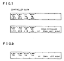
- the controller 40 ⁇ further includes a right switch 416 and a left switch 418. Therefore, controller data as shown in Figure 7 is inputted to the game machine 20 ⁇ from the controller 40 ⁇ .
- the adapter 10 ⁇ is an adapter for making the memory cartridge 30 ⁇ for the game machine 30 ⁇ 0 ⁇ to be applied to the game machine 30 ⁇ , and the same includes a 32-pin connector 10 ⁇ 2 similar to the 32-pin connector 30 ⁇ 8 of the game machine 30 ⁇ 0 ⁇ .
- the memory cartridge 30 ⁇ which incorporates the external memory 32 is detachably attached to the 32-pin connector 10 ⁇ 2.
- the connector 10 ⁇ 2, which is one example of a first connection portion, is connected to a game process circuit 10 ⁇ 4 via data bus and address bus (control bus is omitted in Figure 8) similar to the control bus 332, the address bus 336 and the data bus 340 ⁇ of the game machine shown in Figure 3.
- the game process circuit 10 ⁇ 4 has structure approximately the same as that the game process circuit 324 of the game machine 30 ⁇ 0 ⁇ shown in Figure 3, and therefore, the CPU 326, the oscillating circuit 352, the LCD controller 362, and the sound circuit 378 and etc. included in the game process circuit 10 ⁇ 4. Then, the game process circuit 10 ⁇ 4 and a working RAM 10 ⁇ 6 are coupled to each other by buses. Therefore, when the memory cartridge 30 ⁇ is attached to the connector 10 ⁇ 2, the game process circuit 10 ⁇ 4 is coupled to the external memory 32 of the memory cartridge 30 ⁇ via the buses.
- a VRAM 10 ⁇ 8 is further coupled to the game process circuit 10 ⁇ 4, and the VRAM 10 ⁇ 8 includes the same memory structure as that of the VRAM included in the LCD display RAM 366 of the game machine 30 ⁇ 0 ⁇ shown in Figure 3.
- the game process circuit 10 ⁇ 4 executes the game according to the program stored in the external memory 32.
- the controller data as shown in Figure 7 being transferred from the game machine 20 ⁇ which is shown in Figure 10 ⁇ in detail is applied to a controller interface 112 via a data bus 110 ⁇ . Therefore, the controller interface 112 converts the controller data shown in Figure 7 into controller data which is the same as the controller data from the cross-key switch 312, push button switches 314 and 316, the start switch 318 and the select switch 320 ⁇ of the game machine 30 ⁇ 0 ⁇ shown in Figure 9.
- the controller 40 ⁇ ( Figure 1) of the game machine 20 ⁇
- the movement and the action of the game character displayed on the monitor television (not shown) can be controlled.
- the game process circuit 10 ⁇ 4 outputs the sound signal and the video image data (dot signal) in accordance with the progress of the game, and the clock signal.
- the game process circuit 10 ⁇ 4 generates the video image data of the dots having different luminance or contrast; however, the game process circuit 10 ⁇ 4 may generate video image data of dots having different color tones.
- the sound signal from the game process circuit 10 ⁇ 4 is directly sent to the game machine 20 ⁇ ( Figure 10 ⁇ ) via a connector 113 which is one example of a second connection portion and is for detachably connecting the adapter 10 ⁇ to the game machine 20 ⁇ .
- the image data (dot data) is sent to a digital video signal interface 114.
- the digital video data interface 114 converts the video image data representative of one of four gradations (2 bits) for 8 dots in the horizontal direction, being applied from the game process circuit 10 ⁇ 4 in a bit-serial fashion, into bit parallel data of 2 byte, which is then stored in a buffer RAM 116.
- the digital video data interface 114 converts the video data for 8 dots in the horizontal direction into bit parallel data of 3 byte, which is then stored in the buffer RAM 116. At that time, the gradation data or the color tone data is converted into data of a type of character data for the game machine 20 ⁇ , and then, the character data is sequentially stored in the buffer RAM.
- a video signal for a raster-scan monitor television (not shown) can be outputted from the game machine 20 ⁇ .
- the game machine 20 ⁇ includes a CPU 20 ⁇ 4 and a PPU 20 ⁇ 6.
- the CPU 20 ⁇ 4 and the PPU 20 ⁇ 6 are connected to the data bus 114 and the address bus 118 of the adapter 10 ⁇ via data bus 20 ⁇ 8, and an address bus 210 ⁇ , the connector 20 ⁇ 2, and a connector 113 ( Figure 8).
- a working RAM 212 which is also coupled to the data buses 20 ⁇ 8 and 210 ⁇ .
- the CPU 20 ⁇ 4 receives the controller data from the controller 40 ⁇ .
- the PPU 20 ⁇ 6 outputs by cooperating with a character RAM 214 and a CGRAM (Color Generator RAM) 216 video image data which can be displayed on a raster-scan type display on the basis of the character data applied from the digital video data interface 114 of the adapter 10 ⁇ , i.e., the buffer RAM 116.
- the video image data is applied to a video encoder 218.
- a video image signal from the video encoder 218 is applied to an RF modulator 220 ⁇ , or an output terminal 222.
- the game machine 20 ⁇ is provided with a sound CPU 224, a sound DSP (digital signal processor) 226 and a sound RAM 228, and sound signal from the sound DSP 226 or the sound signal which is applied from the game process circuit 10 ⁇ 4 of the adapter 10 ⁇ via the connector 20 ⁇ 2 is amplified by an amplifier 230 ⁇ , and then, applied to the RF modulator 220 ⁇ or the output terminal 222.
- a sound CPU 224 a sound DSP (digital signal processor) 226 and a sound RAM 228, and sound signal from the sound DSP 226 or the sound signal which is applied from the game process circuit 10 ⁇ 4 of the adapter 10 ⁇ via the connector 20 ⁇ 2 is amplified by an amplifier 230 ⁇ , and then, applied to the RF modulator 220 ⁇ or the output terminal 222.
- a sound DSP digital signal processor
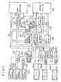
- the controller interface 112 and the digital video data interface 114 included in the adapter 10 ⁇ are shown in Figure 11 in detail.
- the controller interface 112 includes a controller data write register 124 to which the controller data sent from the CPU 20 ⁇ 4 of the game machine 20 ⁇ is loaded through the data bus 110 ⁇ .
- the controller data loaded in the controller data write register 124 is applied to a data selector 126 and a reset signal generating circuit 128.
- the data selector 126 outputs the data loaded in the register 124 onto an input terminal 10 ⁇ 4a of the game process circuit 10 ⁇ 4.
- the data selector 126 selectively derives the signal from the A button switch 40 ⁇ 8, B button switch 410 ⁇ , the select switch 412, the start switch 414 and the cross-key switch 40 ⁇ 2, and then, arranges the signals according to an order of the data format shown in Figure 9, and thereafter, outputs the controller data by four (4) bits in response to a signal from an output terminal 10 ⁇ 4b of the game process circuit 10 ⁇ 4.
- the controller data is applied to the reset circuit 128 which includes a NAND circuit, for example, and applies a reset signal to a reset terminal 10 ⁇ 4c of the game process circuit 10 ⁇ 4 (which is a terminal for inputting a reset signal shown in Figure 4) when a predetermined condition is satisfied by the controller data.
- the reset circuit 128 which includes a NAND circuit, for example, and applies a reset signal to a reset terminal 10 ⁇ 4c of the game process circuit 10 ⁇ 4 (which is a terminal for inputting a reset signal shown in Figure 4) when a predetermined condition is satisfied by the controller data.
- the digital video data interface 114 receives the clock pulse (CP) from an output terminal 10 ⁇ 4d of the game process circuit 10 ⁇ 4, and the dot data DT0 ⁇ and DT1 from output terminals 10 ⁇ 4e and 10 ⁇ 4f of the game process circuit 10 ⁇ 4.
- the dot data DT0 ⁇ from the output terminal 10 ⁇ 4e is loaded in an 8-bit shift register 128.
- the dot data DT1 from the output terminal 10 ⁇ 4f is loaded in an 8-bit shift register 130 ⁇ .
- the shift registers 128 and 138 are utilized for converting the dot data DT0 ⁇ and DT1 which are respectively outputted in a bit-serial fashion into the character data of 8 bits in a bit parallel fashion, and operated in response to the clock pulse (CP).
- the dot data DT0 ⁇ and DT1 are loaded in the shift registers 128 and 130 ⁇ , respectively.
- the dot data DT0 ⁇ and DT1 are latched by data latches 134 and 136 in response to a latch signal applied from a write address counter 132 so as to become character data.
- the character data latched by the data latches 134 and 136 are applied to a data selector 138.
- the video image data having the gradation represented by 2 bits is generated by the game process circuit 10 ⁇ 4; however, even if the video data having the color tone represented by 3 bits is outputted from the game process circuit 10 ⁇ 4, in a similar manner, the dot data of a bit-serial fashion can be converted into 8-bit character data of a bit-parallel fashion.
- the digital video data interface 114 receives the dot data DT0 ⁇ , the dot data DT1 and the dot data DT2 (not shown) respectively corresponding to red, green and blue from the output terminal 10 ⁇ 4e, the output terminal 10 ⁇ 4f and a further output terminal (not shown), and the dot data DT0 ⁇ -DT2 are respectively loaded in the shift register 128, the shift register 138 and a further shift register (not shown).
- the dot data each being for 8 dots are loaded in the respective shift registers
- outputs from the shift registers are latched by the data latch 134, the data latch 136 and a further data latch (not shown), and then, applied to the data selector 138 as character data.
- the write address counter 132 is incremented in response to the clock pulse (CP) applied from the game process circuit 10 ⁇ 4 so as to generate a write address of 14 bits. Therefore, the above described latch signal is applied to the latches 134 and 136 at every timing that the write address counter 132 counts 8 clock pulses (CP). Accordingly, the 8-bit dot data DT0 ⁇ and DT1 (character data) of a bit parallel fashion are applied from the data latches 134 and 136 to the data selector 138.
- a least significant bit A0 ⁇ of the write address counter 132 and an inverted signal /A0 ⁇ (in this specification, "/" is a bar symbol that means an inverted signal) are applied to the data selector 138 as enable signals DT0 ⁇ EN and DT1EN.
- the write address from the write address counter 132 is applied to an address selector 142 through an address bus 140 ⁇ , and a block number register 144. Furthermore, the character data selectively outputted by the data selector 134 is applied to the buffer RAM 116 through a data bus 146.
- a memory format of the game machine 30 ⁇ 0 ⁇ is shown in Figure 6, but the VRAM format of Figure 6 indicates only a given plane of one background picture.
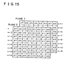
- two sheets of planes i.e. a plane PL0 ⁇ and a plane PL1 are formed in the VRAM to display the gradation represented by the 2 bits, as shown in Figure 12 or Figure 15.
- the dot data DT0 ⁇ is dot data of a front plane PL0 ⁇
- the dot data DT1 is dot data of a rear plane PL1.
- the two shift registers 128 and 138 are utilized for individually converting the two dot data DT0 ⁇ and DT1 into the character data, and by selecting the character data by the data selector 138, the character data for the two sheets of planes PL0 ⁇ and PL1 are written in the buffer RAM 116. Furthermore, in a case where the dot data DT0 ⁇ , DT1 and DT2 (not shown) respectively corresponding to red, green and blue are outputted by the game process circuit 10 ⁇ 4, three sheets of planes PL0 ⁇ , PL1 and PL2 (not shown) are formed in the VRAM in corresponding to red, green and blue.
- the dot data DT0 ⁇ -DT2 generated on the basis of the respective planes are subjected to a serial-parallel conversion by the shift registers, and the character data are selected by the data selector, whereby the character data for the three sheets of planes PL0 ⁇ , PL1 and PL2 (not shown) are written in the buffer RAM 116.
- the block number register 144 shown in Figure 11 decodes the write address from the write address counter 132 and applies a block number corresponding to the write address to the game machine 20 ⁇ through the data bus 110 ⁇ .
- a storage capacity of the buffer RAM 116 is approximately 1/4 of a storage capacity of the VRAM, and therefore, the buffer RAM 116 is read-out by the game machine 20 ⁇ at every time that one of the blocks shown in Figure 13 is completed. Therefore, the storage capacity of the buffer RAM 116 may be small.
- the buffer RAM 116 may have a storage capacity for a single block.
- the data transmission from the buffer RAM 116 to the working RAM 212 can not be performed during a time when the CPU 20 ⁇ 4 of the game machine 20 ⁇ executes an interrupt NMI (described later) having a highest priority. Therefore, in view of the character data (for approximately 1.7-1.8 blocks) stored in the buffer RAM 116 in executing the interrupt NMI, it is desirable that the buffer RAM 116 has a storage capacity of four blocks.
- address data is applied to an address decoder 148 from the game machine 20 ⁇ via an address bus 118.
- the address decoder 148 decodes the address data, and outputs signals RD1, RD2, RD3 and RD4.
- the signal RD3 from the address decoder 148 is applied to a read address counter 150 ⁇ which is incremented at a timing that the signal RD3 is received, and outputs a read address for the buffer RAM 116.
- the read address is applied to an address selector 142 which receives the signal RD4 from the address decoder 148, and selectively applies the write address from the write address counter 132 or the read address from the read address counter 150 ⁇ to the buffer RAM 116.
- the write address is, of course, selected, and at a time that the character is to be read from the buffer RAM 116 to the game machine 20 ⁇ , the read address is selected. Therefore, the write signal (W) from the write address counter 132, and the read signal (R) from the address decoder 148 are respectively applied to the buffer RAM 116. Then, the data read-out from the buffer RAM 116 is loaded in a read data register 152, and then, applied to the game machine 20 ⁇ therefrom via the data bus 110 ⁇ .
- the character read-out the buffer RAM 116 is stored in the working RAM 212 ( Figure 10 ⁇ ) of the game machine 20 ⁇ .
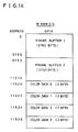
- the working RAM 212 includes a frame buffer area 1, a frame buffer area 2 and color data areas 0 ⁇ -3 as shown in Figure 14.
- a reason why two frame buffer areas 1 and 2 are formed in the working RAM 212 is as follows: In a state where the frame buffer area 1 is completely filled by the character data to be transferred to the character RAM 214, if the character data to be stored in the frame buffer area further occurs, a second frame buffer area is required to store the further character data.
- the frame buffer area 2 is completely filled by the character data to be transferred to the character RAM 214, since the character data of the frame buffer area 1 has been transferred to the character RAM 214, no third frame buffer area is required.
- the character data of the front plane shown in Figure 15 and the character data of the rear plane shown in Figure 15 are alternately stored in accordance with an order that the character data is read-out the buffer RAM 116.
- the dot data DT0 ⁇ of the plane PL0 ⁇ and the dot data DT1 of the plane PL1 shown in Figure 12 are sequentially written.
- the dot data is outputted continuously from a left end dot to a right end dot of the LCD panel 30 ⁇ 4 and in synchronous with a line of the horizontal direction.
- the character data is stored in a character data format as shown in Figure 15 in the frame buffer areas. More specifically, in succeeding to the character data for 8 dots in the horizontal direction of the plane PL0 ⁇ , which is stored in an n-th address of the frame buffer area, in an (n+1)th address, the character data for 8 dots in the horizontal direction of the plane PL1 at the same horizontal position and the same horizontal line as that of the character data stored in the n-th address are stored.
- the write address counter 132 which receives the clock pulse (CP) includes an X address counter 132x and a Y address counter 132y, the former being incremented by the clock pulse (CP), and the latter being incremented in response to a carry signal from the X address counter 132x.
- Address data of 6 bits is outputted from the X address counter 132x, and address data of 8 bits is outputted from the Y address counter 132y.
- a least significant bit A0 ⁇ of the address data from the X address counter 132x is applied to the address selector 142 as the least significant bit A0 ⁇ of the write address.
- bits A1-A5 of the X address counter 132x are latched by an address latch 133x
- 3 bits A6-A8 of the Y address counter 132y are latched by an address latch 133y.
- the 3 bits A6-A8 latched by the address latch 133y are applied as a lower order bits A1-A3 of the write address
- the bits A1-A5 latched by the address latch 133x are applied as upper order bits A4-A8.
- 2 bits A9 and A10 ⁇ out of the remaining bits A9-A13 of the Y address counter 132y are applied as uppermost bits of the write address.
- the bits A9-A13 from the Y address counter 132y are applied to the block number register 144.
- the bit A9 is applied to the game machine 20 ⁇ ( Figure 11) as an interrupt request signal IRQ.
- address A0 ⁇ -A10 ⁇ from the read address counter 150 ⁇ ( Figure 11) is applied to the address selector 142.
- an address conversion is performed, and the character data of the plane PL0 ⁇ and the character data of the plane PL1 are written in the respective block memory areas ( Figure 13) for each block. Therefore, by reading-out the buffer RAM 116 by the read address from the read address counter 150 ⁇ which is sequentially incremented, the character data of the plane PL0 ⁇ and the character data of the plane PL1 shown in Figure 15 are written in one of the frame buffer area 1 and the frame buffer area 2 of the working RAM 212 ( Figure 14) in a character data format on the basis of a data amount of the character data stored in the frame buffer area 1.
- the controller data is automatically read-in with a predetermined time interval by a hardware read-in circuit (not shown) provided in the CPU 20 ⁇ 4 of the game machine 20 ⁇ , for example, and temporarily stored in a controller register (not shown). Therefore, in the step S7, the controller data temporarily stored in the controller register may be simply transferred to the adapter 10 ⁇ .
- the controller interface 112 ( Figure 8) of the adapter 10 ⁇ converts the control data as applied into the same controller data as that of the game machine 30 ⁇ 0 ⁇ so as to apply the same to the game process circuit 10 ⁇ 4.
- the CPU 20 ⁇ 4 selects arbitrarily color data from color data which are set in advance in the program ROM 122 provided in the adapter 10 ⁇ , and fetches the same in the color data area ( Figure 14) of the working RAM 212. That is, the LCD panel 30 ⁇ 4 of the "Game Boy (trademark)” is a monochrome display, while the game machine 20 ⁇ such as "Super NES (trademark)” applies a color video signal to a color monitor television. Therefore, it is necessary to add the color data to the monochrome video data.
- the program ROM 122 is provided in the adapter 10 ⁇ , and color data combinations of m sets being selectable are stored in advance in the program ROM 122, and according to a selection by the player who utilizes the game machine 20 ⁇ or a predetermined method set in advance, any one of the color data combinations of m is selected from the program ROM 122 and the same is written in the working RAM 212.
- the color data may be added such that arbitrary colors out of the same number of colors as that of the game machine 20 ⁇ can be displayed.
- the CPU 20 ⁇ 4 executes an interrupt process shown in Figure 19. Since the interrupt request signal IRQ is the second most significant bit A9 of the write address as described in the above, a fact that the signal IRQ is outputted means that the character data is completely stored in one block of the buffer RAM 116 shown in Figure 13. Therefore, the game machine 20 ⁇ becomes to execute an operation shown in Figure 19 at every time that the character data is completely written in the block area of the buffer RAM 116.
- a content of the block buffer i.e., the block area of the buffer RAM 116 in which the character data is completely written is transferred to the frame buffer, i.e., the frame buffer area 1 or the frame buffer area 2 of the working RAM 212 by means of a direct memory access (DMA).
- the block number data from the block number register 144 is read-in.
- the character data and the color data are stored in the working RAM 212.
- the CPU 20 ⁇ 4 executes an operation shown in Figure 20 ⁇ . More specifically, in response to the interrupt signal NMI, in a step S19 of Figure 20 ⁇ , the CPU 20 ⁇ 4 transfers a content of the frame buffer area of the working RAM 212 in which the character data has been stored to the character RAM 214 ( Figure 10 ⁇ ) by means of the DMA.
- a next step S21 the CPU 20 ⁇ 4 transfers the four color data being stored in the color data area of the working RAM 212 to the CGRAM 216 ( Figure 10 ⁇ ).
- Each of the color data 0 ⁇ to the color data 3 is data of 16 bits.
- the V flag is set, and then, the process returns to the main routine.
- the writing the data from the game process circuit 10 ⁇ 4 ( Figure 8) in the buffer RAM 116 and the reading the data from the buffer RAM 116 by the game machine 20 ⁇ can be simultaneously performed, a time of the write signal (shown in Figure 21) from the write address counter 132 is made sufficiently longer than a time of the read signal from the address decoder 148. Therefore, during a time that the data transfer is performed according to the DMA by the game machine 20 ⁇ is performed, the write operation to the buffer RAM 216 is temporarily stopped for a time of the read signal R; however, since the time of the write signal W is sufficiently long, the writing the data into the buffer RAM 116 is not hindered by the reading of the data. Accordingly, the character data of the blocks can be surely written in the buffer RAM 116. Furthermore, in order to make the buffer RAM 116 possible to store the character data applied from the data selector 138 during the process of the NMI interrupt, the buffer RAM 116 has a storage capacity of 4 blocks as described above.
- the character data is stored in the character RAM as shown in Figure 20 ⁇ , and the color data is stored in the CGRAM, and therefore, the data of the character having the color data is outputted by the PPU ( Figure 10 ⁇ ), and the same is encoded by the video encoder 218, whereby the color video signal is outputted from the game machine 20 ⁇ .
Landscapes
- Engineering & Computer Science (AREA)
- Theoretical Computer Science (AREA)
- Human Computer Interaction (AREA)
- Physics & Mathematics (AREA)
- General Engineering & Computer Science (AREA)
- General Physics & Mathematics (AREA)
- Controls And Circuits For Display Device (AREA)
- Digital Computer Display Output (AREA)
Applications Claiming Priority (6)
| Application Number | Priority Date | Filing Date | Title |
|---|---|---|---|
| JP20473993 | 1993-07-27 | ||
| JP20473993 | 1993-07-27 | ||
| JP204739/93 | 1993-07-27 | ||
| JP6104/94 | 1994-01-25 | ||
| JP610494 | 1994-01-25 | ||
| JP00610494A JP3366413B2 (ja) | 1993-07-27 | 1994-01-25 | 表示情報変換装置および情報処理システム |
Publications (3)
| Publication Number | Publication Date |
|---|---|
| EP0636966A2 true EP0636966A2 (fr) | 1995-02-01 |
| EP0636966A3 EP0636966A3 (fr) | 1996-10-16 |
| EP0636966B1 EP0636966B1 (fr) | 2000-05-10 |
Family
ID=26340182
Family Applications (1)
| Application Number | Title | Priority Date | Filing Date |
|---|---|---|---|
| EP94305558A Expired - Lifetime EP0636966B1 (fr) | 1993-07-27 | 1994-07-27 | Dispositif pour la conversion d'information d'affichage |
Country Status (8)
| Country | Link |
|---|---|
| US (1) | US5552799A (fr) |
| EP (1) | EP0636966B1 (fr) |
| JP (1) | JP3366413B2 (fr) |
| KR (1) | KR950003967A (fr) |
| CN (1) | CN1087639C (fr) |
| AU (1) | AU681153B2 (fr) |
| CA (1) | CA2128798A1 (fr) |
| DE (1) | DE69424347T2 (fr) |
Cited By (2)
| Publication number | Priority date | Publication date | Assignee | Title |
|---|---|---|---|---|
| US5599232A (en) * | 1992-05-02 | 1997-02-04 | Codemasters Limited | Memory cartridge with interface having graphics co-processor |
| GB2380645A (en) * | 2001-09-10 | 2003-04-09 | Mark Technology Corp Q | Picture video signal converting/processing circuit for handheld game systems |
Families Citing this family (55)
| Publication number | Priority date | Publication date | Assignee | Title |
|---|---|---|---|---|
| US6222525B1 (en) | 1992-03-05 | 2001-04-24 | Brad A. Armstrong | Image controllers with sheet connected sensors |
| US6906700B1 (en) | 1992-03-05 | 2005-06-14 | Anascape | 3D controller with vibration |
| US5778421A (en) * | 1992-11-26 | 1998-07-07 | Nintendo Co., Ltd. | Information processing system which can check disk-like storage medium having prescribed relation therewith and disk-like storage medium therefor |
| BR9606363A (pt) | 1995-05-10 | 1997-10-28 | Nintendo Co Ltd | Controlador de máquina de jogar e dispositivo operacional |
| JPH0926761A (ja) * | 1995-07-13 | 1997-01-28 | Nintendo Co Ltd | 画像表示装置 |
| WO1997014088A1 (fr) | 1995-10-09 | 1997-04-17 | Nintendo Co., Ltd. | Systeme de traitement d'images tridimensionnelles |
| JPH09155065A (ja) * | 1995-12-12 | 1997-06-17 | Hudson Soft Co Ltd | 特定固有データ交換可能な対戦型コンピュータゲームシステム |
| US8674932B2 (en) | 1996-07-05 | 2014-03-18 | Anascape, Ltd. | Image controller |
| US6351205B1 (en) * | 1996-07-05 | 2002-02-26 | Brad A. Armstrong | Variable-conductance sensor |
| JP3655438B2 (ja) | 1997-07-17 | 2005-06-02 | 任天堂株式会社 | ビデオゲームシステム |
| JPH11144040A (ja) * | 1997-11-05 | 1999-05-28 | Nintendo Co Ltd | 携帯形ゲーム機および携帯形ゲーム機用カートリッジ |
| JPH11207034A (ja) * | 1997-11-20 | 1999-08-03 | Nintendo Co Ltd | 異なる種類のゲーム機間でバックアップデータを利用して プレイ可能なゲームシステム |
| JPH11155150A (ja) | 1997-11-20 | 1999-06-08 | Nintendo Co Ltd | 映像信号ディジタル処理装置、映像信号ディジタル処理のための情報記憶媒体、および映像信号ディジタル処理方法 |
| JPH11253660A (ja) * | 1998-03-13 | 1999-09-21 | Bandai Co Ltd | ゲーム機、該ゲーム機の起動方法及び該ゲーム機用ゲームプログラムの実行方法 |
| US6315669B1 (en) | 1998-05-27 | 2001-11-13 | Nintendo Co., Ltd. | Portable color display game machine and storage medium for the same |
| JP3874536B2 (ja) * | 1998-05-27 | 2007-01-31 | 任天堂株式会社 | 携帯型カラー表示ゲーム機およびその記憶媒体 |
| WO2000030067A1 (fr) * | 1998-11-17 | 2000-05-25 | Quantum3D, Inc. | Systeme, procede et dispositif d'adaptation de jeux d'arcade anciens |
| JP2000300851A (ja) * | 1999-02-16 | 2000-10-31 | Konami Co Ltd | ゲームシステム並びにそのゲームシステムで使用可能なゲーム装置およびコンピュータ読み取り可能な記憶媒体 |
| USD432586S (en) * | 1999-07-27 | 2000-10-24 | Cristiano Galli-Zugaro | Game case |
| USD434455S (en) * | 1999-08-12 | 2000-11-28 | Kabushiki Kaisha Toshiba | Digital video disk player |
| US6743104B1 (en) | 1999-11-18 | 2004-06-01 | Nintendo Co., Ltd. | Portable game machine |
| US6373462B1 (en) | 1999-12-07 | 2002-04-16 | Nintendo Co., Ltd. | Method and apparatus for displaying higher color resolution on a hand-held LCD device |
| KR20020060069A (ko) * | 1999-11-24 | 2002-07-16 | 야마우치 히로시 | 휴대용 lcd 장치에 고 칼러 분해능을 표시하는 방법 및장치 |
| US7050064B2 (en) * | 1999-11-24 | 2006-05-23 | Nintendo Co., Ltd. | Method and apparatus for displaying higher color resolution on a hand-held LCD device |
| JP4550374B2 (ja) * | 2000-02-25 | 2010-09-22 | 株式会社ソニー・コンピュータエンタテインメント | 画像出力装置に応じた画像データを作成する情報処理装置およびそのための記録媒体 |
| JP3474173B2 (ja) * | 2000-02-25 | 2003-12-08 | 株式会社ソニー・コンピュータエンタテインメント | 画像出力装置に応じた画像データを作成する情報処理装置およびそのための記録媒体 |
| US6955606B2 (en) * | 2000-03-30 | 2005-10-18 | Nintendo Co., Ltd. | Game information storage medium and game system using the same |
| US6894686B2 (en) | 2000-05-16 | 2005-05-17 | Nintendo Co., Ltd. | System and method for automatically editing captured images for inclusion into 3D video game play |
| US6810463B2 (en) * | 2000-05-24 | 2004-10-26 | Nintendo Co., Ltd. | Gaming machine that is usable with different game cartridge types |
| US7445551B1 (en) | 2000-05-24 | 2008-11-04 | Nintendo Co., Ltd. | Memory for video game system and emulator using the memory |
| US7285051B2 (en) * | 2000-05-25 | 2007-10-23 | Nintendo Co., Ltd. | Game information storage medium and game system using the same |
| US8157654B2 (en) | 2000-11-28 | 2012-04-17 | Nintendo Co., Ltd. | Hand-held video game platform emulation |
| US6672963B1 (en) | 2000-09-18 | 2004-01-06 | Nintendo Co., Ltd. | Software implementation of a handheld video game hardware platform |
| US6884171B2 (en) | 2000-09-18 | 2005-04-26 | Nintendo Co., Ltd. | Video game distribution network |
| US6439956B1 (en) | 2000-11-13 | 2002-08-27 | Interact Accessories, Inc. | RC car device |
| JP4623841B2 (ja) * | 2001-02-21 | 2011-02-02 | 任天堂株式会社 | 互換性を有するゲーム機に利用されるゲームプログラム |
| US20040014528A1 (en) * | 2002-07-16 | 2004-01-22 | Richard Leifer | Memory retrofit apparatus for portable game devices |
| KR20050050643A (ko) * | 2002-08-14 | 2005-05-31 | 코닌클리케 필립스 일렉트로닉스 엔.브이. | 수집 가능한 오브젝트를 사용한 원격 제어 |
| US8016681B2 (en) * | 2004-03-31 | 2011-09-13 | Nintendo Co., Ltd. | Memory card for a game console |
| US8267780B2 (en) * | 2004-03-31 | 2012-09-18 | Nintendo Co., Ltd. | Game console and memory card |
| US11278793B2 (en) | 2004-03-31 | 2022-03-22 | Nintendo Co., Ltd. | Game console |
| US7771280B2 (en) * | 2004-03-31 | 2010-08-10 | Nintendo Co., Ltd. | Game console connector and emulator for the game console |
| US7837558B2 (en) | 2004-03-31 | 2010-11-23 | Nintendo Co., Ltd. | Game console and emulator for the game console |
| KR100601047B1 (ko) * | 2004-12-16 | 2006-07-18 | 한국전자통신연구원 | 임베디드 시스템에서 동영상 및 스킨 합성 장치 및 그 방법 |
| CN100595772C (zh) * | 2004-12-30 | 2010-03-24 | 英业达股份有限公司 | 执行网络游戏的方法 |
| US20070010323A1 (en) * | 2005-07-05 | 2007-01-11 | International Business Machines Corporation | Platform-adaptive gaming |
| JP4920942B2 (ja) * | 2005-10-04 | 2012-04-18 | 任天堂株式会社 | ゲームシステム |
| JP2010509992A (ja) | 2006-11-17 | 2010-04-02 | 任天堂株式会社 | ビデオゲームプログラムのダウンロードシステムおよびダウンロード方法 |
| USD613341S1 (en) | 2009-07-28 | 2010-04-06 | Hyperkin Inc. | Video game console |
| JP5122659B2 (ja) * | 2011-01-07 | 2013-01-16 | 任天堂株式会社 | 情報処理プログラム、情報処理方法、情報処理装置及び情報処理システム |
| USD677280S1 (en) * | 2011-10-14 | 2013-03-05 | Blackmagic Design Pty Ltd | Video converter |
| AU344698S (en) | 2012-04-13 | 2012-10-05 | Blackmagic Design Pty Ltd | Video converter |
| USD727360S1 (en) * | 2013-09-24 | 2015-04-21 | Western Digital Technologies, Inc. | Media player |
| JP2017144218A (ja) * | 2016-02-19 | 2017-08-24 | 株式会社コーエーテクモゲームス | ゲームシステム、ゲーム装置、情報処理装置および制御プログラム |
| US20250005704A1 (en) * | 2023-06-28 | 2025-01-02 | Texas Instruments Incorporated | Methods and apparatus to animate a splash screen |
Family Cites Families (10)
| Publication number | Priority date | Publication date | Assignee | Title |
|---|---|---|---|---|
| GB2115989B (en) * | 1982-02-12 | 1985-08-14 | Voltmace Limited | Programmed cartridge/video machine adaptor |
| JPH0782306B2 (ja) * | 1986-05-30 | 1995-09-06 | 株式会社日立製作所 | ビデオインターフェース方法及び装置 |
| JPH07100088B2 (ja) * | 1986-11-07 | 1995-11-01 | 任天堂株式会社 | ゲ−ム機用カ−トリツジのアダプタ |
| US5112051A (en) * | 1989-06-05 | 1992-05-12 | Westinghouse Electric Corp. | Interfacing device for a computer games system |
| JPH04176235A (ja) * | 1990-11-08 | 1992-06-23 | Nintendo Co Ltd | ゲーム機用通信アダプタ |
| US5203848A (en) * | 1992-01-16 | 1993-04-20 | Myson Technology, Inc. | Television game console and electronic control device for controlling the allowable playing time of the television game console |
| US5388841A (en) * | 1992-01-30 | 1995-02-14 | A/N Inc. | External memory system having programmable graphics processor for use in a video game system or the like |
| CA2074388C (fr) * | 1992-01-30 | 2003-01-14 | Jeremy E. San | Processeur graphique programmable a logiciel de conversion de pixels en caracteres pour jeux video ou systemes similaires |
| GB9210786D0 (en) * | 1992-05-20 | 1992-07-08 | Codemasters Ltd | Memory cartridges |
| US5282621A (en) * | 1992-11-24 | 1994-02-01 | Tseng Ching J | Universal converter for non-exclusive cards of video game |
-
1994
- 1994-01-25 JP JP00610494A patent/JP3366413B2/ja not_active Expired - Lifetime
- 1994-07-25 KR KR1019940018383A patent/KR950003967A/ko not_active Withdrawn
- 1994-07-25 US US08/280,207 patent/US5552799A/en not_active Expired - Fee Related
- 1994-07-26 CA CA002128798A patent/CA2128798A1/fr not_active Abandoned
- 1994-07-27 AU AU68723/94A patent/AU681153B2/en not_active Ceased
- 1994-07-27 DE DE69424347T patent/DE69424347T2/de not_active Expired - Lifetime
- 1994-07-27 EP EP94305558A patent/EP0636966B1/fr not_active Expired - Lifetime
- 1994-07-27 CN CN94108713A patent/CN1087639C/zh not_active Expired - Fee Related
Cited By (2)
| Publication number | Priority date | Publication date | Assignee | Title |
|---|---|---|---|---|
| US5599232A (en) * | 1992-05-02 | 1997-02-04 | Codemasters Limited | Memory cartridge with interface having graphics co-processor |
| GB2380645A (en) * | 2001-09-10 | 2003-04-09 | Mark Technology Corp Q | Picture video signal converting/processing circuit for handheld game systems |
Also Published As
| Publication number | Publication date |
|---|---|
| KR950003967A (ko) | 1995-02-17 |
| CN1105130A (zh) | 1995-07-12 |
| AU681153B2 (en) | 1997-08-21 |
| EP0636966A3 (fr) | 1996-10-16 |
| CA2128798A1 (fr) | 1995-01-28 |
| CN1087639C (zh) | 2002-07-17 |
| US5552799A (en) | 1996-09-03 |
| JPH0792943A (ja) | 1995-04-07 |
| AU6872394A (en) | 1995-02-09 |
| EP0636966B1 (fr) | 2000-05-10 |
| JP3366413B2 (ja) | 2003-01-14 |
| DE69424347D1 (de) | 2000-06-15 |
| DE69424347T2 (de) | 2001-02-08 |
Similar Documents
| Publication | Publication Date | Title |
|---|---|---|
| US5552799A (en) | Display information conversion apparatus | |
| EP0473390B1 (fr) | Superposition d'images fixes formées des caractères | |
| US6373462B1 (en) | Method and apparatus for displaying higher color resolution on a hand-held LCD device | |
| US20020039924A1 (en) | Portable color display game machine and storage medium for the same | |
| US6369827B1 (en) | Method and apparatus for displaying higher color resolution on a hand-held LCD device | |
| JPH07204349A (ja) | ゲーム機用変換装置 | |
| EP0590785B1 (fr) | Appareil de traitement de données de sons et d'images | |
| US5459485A (en) | Image and sound processing apparatus | |
| JP2761335B2 (ja) | 画面表示装置 | |
| US7050064B2 (en) | Method and apparatus for displaying higher color resolution on a hand-held LCD device | |
| CA1234436A (fr) | Dispositif d'alimentation en signaux de donnees pour systeme d'affichage de donnees | |
| US4871167A (en) | General purpose display controller for electronic games | |
| JPS6235140B2 (fr) | ||
| JP3479502B2 (ja) | ゲーム画像生成制御方法、装置、ゲーム画像生成制御プログラムを記録した可読記録媒体及びビデオゲーム装置 | |
| JP2000296229A (ja) | パチンコ機の画像処理表示装置 | |
| JPH11143447A (ja) | パチンコ機のカラー画像表示装置 | |
| JP2905343B2 (ja) | バックグラウンドアトリビュートテーブルのスタートアドレス指定レジスタ付きコンピュータ装置 | |
| EP0121810A2 (fr) | Microprocesseur | |
| JP2004012514A (ja) | 画像表示装置 | |
| CA2452420A1 (fr) | Appareil de traitement d'images et de sons | |
| JPH07219516A (ja) | 描画装置及びその描画方法 | |
| HK1004509A (en) | Superimpositon of moving characters on generated still pictures | |
| JPS62249188A (ja) | キヤラクタデ−タのデイスプレイ方法および装置 | |
| JPH07213746A (ja) | ゲーム装置 | |
| JPH08328545A (ja) | 画像出力装置 |
Legal Events
| Date | Code | Title | Description |
|---|---|---|---|
| PUAI | Public reference made under article 153(3) epc to a published international application that has entered the european phase |
Free format text: ORIGINAL CODE: 0009012 |
|
| AK | Designated contracting states |
Kind code of ref document: A2 Designated state(s): DE FR GB SE |
|
| PUAL | Search report despatched |
Free format text: ORIGINAL CODE: 0009013 |
|
| AK | Designated contracting states |
Kind code of ref document: A3 Designated state(s): DE FR GB SE |
|
| 17P | Request for examination filed |
Effective date: 19961115 |
|
| 17Q | First examination report despatched |
Effective date: 19980326 |
|
| GRAG | Despatch of communication of intention to grant |
Free format text: ORIGINAL CODE: EPIDOS AGRA |
|
| GRAG | Despatch of communication of intention to grant |
Free format text: ORIGINAL CODE: EPIDOS AGRA |
|
| GRAH | Despatch of communication of intention to grant a patent |
Free format text: ORIGINAL CODE: EPIDOS IGRA |
|
| GRAH | Despatch of communication of intention to grant a patent |
Free format text: ORIGINAL CODE: EPIDOS IGRA |
|
| GRAA | (expected) grant |
Free format text: ORIGINAL CODE: 0009210 |
|
| RIC1 | Information provided on ipc code assigned before grant |
Free format text: 7G 06F 3/14 A, 7G 06F 1/16 B, 7G 09G 5/00 B, 7G 06F 17/00 B, 7A 63F 13/00 B, 7G 06F 161:00 Z |
|
| AK | Designated contracting states |
Kind code of ref document: B1 Designated state(s): DE FR GB SE |
|
| REF | Corresponds to: |
Ref document number: 69424347 Country of ref document: DE Date of ref document: 20000615 |
|
| ET | Fr: translation filed | ||
| PG25 | Lapsed in a contracting state [announced via postgrant information from national office to epo] |
Ref country code: SE Free format text: LAPSE BECAUSE OF FAILURE TO SUBMIT A TRANSLATION OF THE DESCRIPTION OR TO PAY THE FEE WITHIN THE PRESCRIBED TIME-LIMIT Effective date: 20000810 |
|
| PLBE | No opposition filed within time limit |
Free format text: ORIGINAL CODE: 0009261 |
|
| STAA | Information on the status of an ep patent application or granted ep patent |
Free format text: STATUS: NO OPPOSITION FILED WITHIN TIME LIMIT |
|
| 26N | No opposition filed | ||
| REG | Reference to a national code |
Ref country code: GB Ref legal event code: IF02 |
|
| PGFP | Annual fee paid to national office [announced via postgrant information from national office to epo] |
Ref country code: DE Payment date: 20130722 Year of fee payment: 20 |
|
| PGFP | Annual fee paid to national office [announced via postgrant information from national office to epo] |
Ref country code: FR Payment date: 20130722 Year of fee payment: 20 Ref country code: GB Payment date: 20130702 Year of fee payment: 20 |
|
| REG | Reference to a national code |
Ref country code: DE Ref legal event code: R071 Ref document number: 69424347 Country of ref document: DE |
|
| REG | Reference to a national code |
Ref country code: GB Ref legal event code: PE20 Expiry date: 20140726 |
|
| PG25 | Lapsed in a contracting state [announced via postgrant information from national office to epo] |
Ref country code: DE Free format text: LAPSE BECAUSE OF EXPIRATION OF PROTECTION Effective date: 20140729 |
|
| PG25 | Lapsed in a contracting state [announced via postgrant information from national office to epo] |
Ref country code: GB Free format text: LAPSE BECAUSE OF EXPIRATION OF PROTECTION Effective date: 20140726 |