EP0637854A2 - Contact à souder - Google Patents
Contact à souder Download PDFInfo
- Publication number
- EP0637854A2 EP0637854A2 EP94110947A EP94110947A EP0637854A2 EP 0637854 A2 EP0637854 A2 EP 0637854A2 EP 94110947 A EP94110947 A EP 94110947A EP 94110947 A EP94110947 A EP 94110947A EP 0637854 A2 EP0637854 A2 EP 0637854A2
- Authority
- EP
- European Patent Office
- Prior art keywords
- contact
- housing
- solder
- web
- spring arm
- Prior art date
- Legal status (The legal status is an assumption and is not a legal conclusion. Google has not performed a legal analysis and makes no representation as to the accuracy of the status listed.)
- Granted
Links
- 238000005476 soldering Methods 0.000 title claims abstract description 7
- 229910000679 solder Inorganic materials 0.000 claims abstract description 63
- 239000002184 metal Substances 0.000 claims abstract description 5
- 239000011324 bead Substances 0.000 description 8
- 238000004519 manufacturing process Methods 0.000 description 2
- 239000000725 suspension Substances 0.000 description 2
- 238000005452 bending Methods 0.000 description 1
- 230000015572 biosynthetic process Effects 0.000 description 1
- 238000011161 development Methods 0.000 description 1
- 230000018109 developmental process Effects 0.000 description 1
- 238000003780 insertion Methods 0.000 description 1
- 230000037431 insertion Effects 0.000 description 1
- 230000007774 longterm Effects 0.000 description 1
- 230000007704 transition Effects 0.000 description 1
Images



Classifications
-
- H—ELECTRICITY
- H01—ELECTRIC ELEMENTS
- H01R—ELECTRICALLY-CONDUCTIVE CONNECTIONS; STRUCTURAL ASSOCIATIONS OF A PLURALITY OF MUTUALLY-INSULATED ELECTRICAL CONNECTING ELEMENTS; COUPLING DEVICES; CURRENT COLLECTORS
- H01R12/00—Structural associations of a plurality of mutually-insulated electrical connecting elements, specially adapted for printed circuits, e.g. printed circuit boards [PCB], flat or ribbon cables, or like generally planar structures, e.g. terminal strips, terminal blocks; Coupling devices specially adapted for printed circuits, flat or ribbon cables, or like generally planar structures; Terminals specially adapted for contact with, or insertion into, printed circuits, flat or ribbon cables, or like generally planar structures
- H01R12/50—Fixed connections
- H01R12/51—Fixed connections for rigid printed circuits or like structures
- H01R12/55—Fixed connections for rigid printed circuits or like structures characterised by the terminals
- H01R12/58—Fixed connections for rigid printed circuits or like structures characterised by the terminals terminals for insertion into holes
Definitions
- the invention relates to a one-piece solder contact made from a stamped sheet metal part according to the preamble of claim 1.
- solder contact is known from DE 41 03 423 C2.
- the contact point is arranged in these contacts so that it is permanently movable, so that relative movements between a contact pin and the contact point of the solder contact can be prevented by the contact point being movable in particular in the direction of the plug axis and transversely thereto, and thereby the movements of a contact pin or the a printed circuit board can follow soldered solder contact.
- solder contact is relatively large in volume because of the special oscillatable suspension of the contact point.
- a similar solder contact is known from DE 41 09 519 A1, which has an approximately cuboid shape, the contact regions being provided centrally on two opposite side faces, each of which is connected to the end edges of the cuboid contact by meandering cut-out strips.
- the contact point is arranged in the center of the cuboid solder contact and provided with a certain flexibility in the direction of the side walls. The path of a contact pin inserted into such a solder contact is thus through the front edges of the solder contact are limited and the two contact areas held by the meandering strips are each independently movable, so that there is no contact point with a precisely defined distance.
- the object of the invention is to provide a solder contact with a small footprint, which has a movable contact point.
- the contact spring arms forming the contact point are connected to an arc spring arm web, which extends from a housing wall over an arc into the housing, a relatively long arc spring arm web can be provided in a small housing, so that the contact point can be moved, which it enables a contact pin inserted into the contact point to move independently of the housing of the solder contact.
- loosening of the solder contact from a printed circuit board due to vibrations of a contact pin inserted in the contact point is avoided, since only slight movement forces are transmitted from the contact pin via the contact point to the housing of the solder contact soldered onto a printed circuit board.
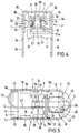
- a first exemplary embodiment of a solder contact according to the invention comprises two side walls 1 and 2 and a top wall 3 (FIGS. 1-5).
- the side walls 1 and 2 are bent at right angles from the top wall 3, so that a kind of downwardly open, cross-sectionally U-shaped housing is formed.
- the top wall 3 has a free, straight trailing edge 4 and a free, semicircular arch leading edge 5.
- a bead 6 running parallel to the rear edge 4 is pressed into the ceiling wall 3, which extends a bit into the side walls 1 and 2, so that the U-shape of the housing is stiffened by the bead 6 against expansion.
- a plug hole 7 of approximately 1.5 mm in diameter is punched out in the top wall 3 for the insertion of an approximately 1 mm thick plug contact pin (not shown).
- a stop tab 8 can be formed in the top wall 3 by a U-shaped free cut 9 facing the hole 7, which is angled at right angles inwards into the housing.
- the side walls 1, 2 have a free straight rear edge 10, 11, a straight front edge 12, 13 and free straight lower edges 14, 15.
- a soldering leg 16 protruding from the edge is connected to each lower edge 14, 15, namely at a short distance from the trailing edge 10 and 11.
- a projecting support tab 17 for supporting the housing on a circuit board 17a is connected at a short distance from each soldering leg 16 , whose function is explained below.
- the side walls 1, 2 can each have a bead 18 running parallel to the rear edge 10, 11 in the region between the soldering leg 16 and the front edge 12 or 13, which respectively extends somewhat into the top wall 3.
- holes 19, 19a are punched out on the longitudinal edges 20 in the transition area between the side walls 1, 2 and the top wall 3, expediently in the area between the beads 6 and 18 and between the bead 18 and the front edge 12 and 13.
- the side wall 2 has a further stop tab 21, which is formed by an incision made parallel to the lower edge 15 at a distance therefrom and made from the front edge 13, the Stop flap 21 is bent at right angles into the housing in such a way that its free longitudinal edge 21a facing the top wall 3 is at a distance below the free longitudinal edge 8a of the stop flap 8.
- stop tabs 8, 21 The function of the stop tabs 8, 21 is explained below.
- a stiffening bead 22 bridging the bend is pressed into the stop flap 21 in the longitudinal extension of the flap; it also has further, laterally spaced support tabs 17 on its lower edge for supporting the stop tab 21 on the printed circuit board 17a.
- the stop tabs 8 and 21 are slightly offset from one another, the stop tab 8 coming closer to the rear edges 10, 11 and the stop tab 21 closer to the front edges 12, 13.
- the function of the relative position of the stop tabs 8, 21 is explained in more detail below.
- the side wall 1 has a rectangular bow spring arm web 23, which is formed by two cuts 24 and 25 made by the rear edge 10 of this side wall and extends approximately centrally between the top wall 3 and the free lower edge 14 of the side wall 1.
- the bow spring arm web 23 is semicircularly curved, and this bow area 26 projects slightly outwards beyond the rear edge 4 of the ceiling wall 3.
- the arch spring arm web 23 runs parallel to the side walls 1 and 2 at a distance therefrom in a plane passing through the ceiling wall 3 closer to the side wall 2.
- a U-shaped spring arm base 28 is connected to the free end of the straight arch spring arm region 27, which has a U-base web 29 which is bent out towards the top wall 3 and has an arc shell line running in the longitudinal direction of the housing and two straight U-legs 30 and 31 running parallel to the side walls 1, 2, which protrude on both sides over the longitudinal edges of the straight bow spring arm region 27 and of which the leg 31 lies in the extension of the straight bow spring arm region 27.
- the spring arm base 28 is equally spaced from the side walls 1, 2 because of the eccentric position of the straight bow spring arm region 27 and lies with its end edges spaced apart from the stop tabs 8, 21.
- In the U-legs 30, 31 and the U-base web 29 there is one continuous, U-shaped Crimp 32 pressed through which the spring arm base 28 is stiffened against expansion.
- Contact spring arms 33 and 34 are connected in one piece to the end edges of the two U-legs 30 and 31 pointing to the front edge 5 of the ceiling wall 3 and define a contact point 35 under the plug hole 7.
- stop lugs 36 to 39 which cooperate with the stop edges 8a and 21a, are angled from the longitudinal edge of the spring arms 33, 34 and extend transversely to the longitudinal extent.
- the spring arm stop flaps 36 to 39 are bent outwards by 90 ° from the spring arms 33, 34 and are spaced with their free transverse edges from the stop edges 8a, 21a, so that the spring arms 33, 34 extend freely through the constriction which passes through the opposite stop tabs 8 and 21 is fixed.
- the incisions defining the stop tabs 36 to 39 are spaced apart in the longitudinal direction of the spring arms 33, 34 in such a way that the spring arm stop tabs 36 to 39 are also at a distance from the stop tabs 8, 21 in this direction.
- the stop tab 8 is closer to the cut free end edges of the U-legs 30, 31 than the tab 21, which in turn is closer to the contact point-side, defined by the incisions of contact areas 40, 41 of the spring arms than the tab 8.
- the mobility of the bow spring arm web 23 is limited upwards and downwards.
- the mobility of the bow spring arm web can be limited laterally by the side wall 1, 2 or by a stop of the rear edges of the contact sections 40, 41 on the stop tabs 21.
- the contact point 35 is defined by the contact areas 40 and 41 of the contact spring arms 33, 34, which connect to the stop tabs 36 to 39 and span the plug hole 7.
- the contact areas 40 and 41 are about the longitudinal center axis of the housing on both sides of this axis to be bent transversely outwards to the side walls 1, 2. This bend stiffens the contact regions 40, 41 and also forms a finding funnel 42 opposite the plug hole 7 and widening towards it. Transverse to their arcuate lines parallel to the longitudinal center axis, the curved contact sections 40, 41 lie opposite each other with a minimal distance and thus form the Contact point 35.
- a rectangular arch spring web 44 is connected to the front edge of the contact area 40, which is narrower than the contact area 40 and which, with its free end 45, engages around the other contact area 41 laterally from the outside, and which lies with its free end edge 43 in a plane which penetrates the center of the hole.
- the section 46, with which the bow spring web 44 rests on the outside of the contact area 41, is to be bent out in a spherical or partially cylindrical manner onto the contact area 41 with a longitudinally extending arc jacket line and forms an abutment, which from outside at the level of the contact point 35 against the contact area 41 presses.
- the arch spring web 44 designed in this way which is connected in one piece to the one contact area 40 and presses externally against the other contact area 41, ensures that when the plug contact pin is inserted into the contact point 35 via the plug hole 7, this pin is held captive in the contact area.
- the soft spring characteristic of the bow spring bar 44 is determined by an elongated hole 47 which extends from its connection area to the contact area 40 to its crowned contact area 45.
- the bow spring bar 44 extends up to close to the front edge 5 of the ceiling wall 3.
- the bow spring bar 44 achieves permanent, fixed contacting of the plug contact pin.
- the Bogenfederarmsteg 23 is also characterized by a soft spring characteristic, which results from its great length and by which the contact point 35 holding the contact pin is permanently movable, so that relative movements between the contact pin and the contact point can be prevented by the contact point being movable in particular in the direction of the plug-in axis and transversely thereto, as a result of which the contact point 35 can follow the movements of the contact pin within the scope of the freedom of movement of the spring arms 33, 34 in the region of their stop tabs 36 to 39 relative to the stop tab 8, 21 fixed to the housing.
- the particularly oscillatable suspension of the contact point 35 is achieved with a small volume of the solder contact due to the long bow spring arm web 23, which, as an alternative to the embodiment described above, can also be extended in that its connection area is inserted even further into the side wall 1 by means of correspondingly deep incisions .
- a second exemplary embodiment of the invention has a bow spring arm web 23 which is formed from two thin bow loops 23a, 23b. These two thin bow loops 23a, 23b significantly increase the resilience and thus the mobility of the contact point defined by the contact spring arms 33, 34 compared to the first embodiment with a strip-shaped bow spring arm web 23.
- This mobility of the contact point 35 makes it possible for a contact pin located in the contact point 35 to move more freely with respect to the housing of the solder contact, in particular to be able to oscillate or vibrate, the electrical contact not being interrupted and the kinetic energy of the contact pin not or only to one very small part is transferred to the housing of the solder contact, so that the solder contact is securely attached to the printed circuit board 17a in the long term.
- the bow region 26 can be bent with a smaller radius, so that when the bow loops are connected with incisions 24 and 25, the bow does not project outward beyond the rear edge 4 of the ceiling wall 3. This ensures lateral protection of the bow loops 23a, 23b and further reduces the overall length of the solder contact.
- FIGS. 6, 7 is identical to the first exemplary embodiment (FIGS. 1 to 5), with the same reference numerals identifying the same parts on the solder contacts.
- a third exemplary embodiment of the invention has a meandering spring arm web 23 (FIG. 12).
- the spring arm web 23 is connected to the side wall 1 with an arch region 50.
- the arch region 50 of the arch spring arm web 23 merges into a meandering area with straight-line regions 51a, 51c and 51e of the arch spring arm web 23, which are connected to each other by narrow arches 51b and 51d.
- This meandering area of the bow spring arm web 23 extends from the area of the connection 50 on the side wall 1 to the rear towards the rear edge 4, the bow spring arm web going into a straight line area 54 which extends perpendicular to the side wall 1 and which is followed by a further bow area 53, which leads approximately into the center of the housing of the solder contact, where the U-shaped spring arm base 28 is connected to the bow spring arm web 23 (FIG. 10).
- the arch spring arm web 23 which runs in such a meandering fashion lies entirely in the region which is delimited by the side walls 1, 2 and the top wall 3.
- the bow spring arm web 23 does not protrude beyond the rear edge 4 of the ceiling wall 3, as is the case with the first embodiment.
- the meandering area of the bow spring arm web 23, which preferably extends from the area of the connection 50 to the bow area 53, gives the bow spring arm web 23 a soft characteristic curve, so that the contact spring point 35 delimited by the two contact spring arms 33, 34 in relation to the housing of the solder contact is almost freely movable, but without the electrical connection made by the contact spring arms 33, 34 via the spring arm base 28, the bow spring arm web 23, the housing with the side walls 1, 2 and the top wall 3 and leads the solder legs 16, is interrupted.
- stop tabs 36 to 39 are formed transversely to the longitudinal direction of the contact spring arms 33, 34.
- These stop flaps 36 to 39 interact with a flap 8 which is cut free by a cutout 9 in the ceiling wall 3 and which limits the movement of the contact spring arms 33, 34 in the direction of the ceiling wall 3 and also cooperate with a web 55 which is connected to the side wall 2 and extends from the side wall 2 to the side wall 1 approximately at right angles to the side walls 1, 2, by means of which the movement of the contact spring arms 33, 34 in the direction away from the top wall 3 is limited.
- the web 55 is preferably located in an incision 57 in the side wall 1, so that its position is fixed, which in this exemplary embodiment is not offset from the tab 8 in the longitudinal direction of the soldering contact.
- the tab 8 and the web 55 are arranged at a distance from the respective stop tabs 36 to 39, so that the contact spring arms 33, 34 have a play up and down.
- the top wall 3 does not extend over the contact point 35, but has a front edge 5 with an arc region 5a, over which the contact spring arms 33, 34 protrude.
- the contact spring arms 33, 34 form contact regions 40 and 41, to which flaps 40a and 41a, which are bent outwards, are connected in order to form a finding funnel for a contact plug pin.
- the contact areas 40, 41 are in turn connected to an arc spring web 44 which is connected to the contact area 41 and presses externally against the other contact area 40.
- a tab 56 is also attached to the contact area 40, which stands obliquely forward in the direction of the opposite contact area 41, so that the contact point 35 is limited at the front.
- the spring characteristic becomes by the formation of the bow spring arm web 23 from bow loops or meandering bow spring arm web 23 Compared to the first embodiment significantly softer, so that the contact point can be moved almost completely independently of the housing of the solder contact and only up and down through the tabs 8, 21 or the tab 8 and the web 55 and laterally through the side walls 1, 2 is limited, against which the tabs 40a, 41a of the contact spring arms 33, 34 abut. Due to the soft characteristic curve, it is also not necessary to reinforce the walls 1, 2 and 3 of the housing by beads or the like, since the forces exerted by a contact pin on the walls via the contact spring arms are very low. This simplifies the manufacturing process and thus reduces the manufacturing costs of the solder contact.
Landscapes
- Coupling Device And Connection With Printed Circuit (AREA)
- Details Of Connecting Devices For Male And Female Coupling (AREA)
- Multi-Conductor Connections (AREA)
Applications Claiming Priority (2)
| Application Number | Priority Date | Filing Date | Title |
|---|---|---|---|
| DE4326456A DE4326456A1 (de) | 1993-08-06 | 1993-08-06 | Lötkontakt |
| DE4326456 | 1993-08-06 |
Publications (3)
| Publication Number | Publication Date |
|---|---|
| EP0637854A2 true EP0637854A2 (fr) | 1995-02-08 |
| EP0637854A3 EP0637854A3 (fr) | 1995-10-25 |
| EP0637854B1 EP0637854B1 (fr) | 1999-01-27 |
Family
ID=6494615
Family Applications (1)
| Application Number | Title | Priority Date | Filing Date |
|---|---|---|---|
| EP94110947A Expired - Lifetime EP0637854B1 (fr) | 1993-08-06 | 1994-07-14 | Contact à souder |
Country Status (4)
| Country | Link |
|---|---|
| US (1) | US5597332A (fr) |
| EP (1) | EP0637854B1 (fr) |
| JP (1) | JPH07320802A (fr) |
| DE (2) | DE4326456A1 (fr) |
Cited By (2)
| Publication number | Priority date | Publication date | Assignee | Title |
|---|---|---|---|---|
| GB2306807A (en) * | 1995-10-24 | 1997-05-07 | Modelec Sa | Socket contact for an electrical connector |
| US5679010A (en) * | 1994-12-20 | 1997-10-21 | The Whitaker Corporation | Anti-fretting terminal for PCB |
Families Citing this family (11)
| Publication number | Priority date | Publication date | Assignee | Title |
|---|---|---|---|---|
| JP3412539B2 (ja) * | 1998-11-30 | 2003-06-03 | 住友電装株式会社 | 電気接続構造 |
| US6511336B1 (en) * | 2000-05-25 | 2003-01-28 | Illinois Tool Works Inc. | Solderless flex termination for motor tab |
| DE102004062879A1 (de) * | 2004-12-27 | 2006-07-06 | Lear Corp., Southfield | Elektrisches Kontaktelement sowie Kontaktierungseinrichtung mit Kontaktelement |
| JP4913539B2 (ja) * | 2006-10-25 | 2012-04-11 | 日本圧着端子製造株式会社 | ソケットコンタクト |
| JP4889118B2 (ja) * | 2007-06-07 | 2012-03-07 | 株式会社ヨコオ | 電気コネクタ |
| US20090109691A1 (en) * | 2007-10-24 | 2009-04-30 | Yung-Yi Chuang | Bent fixing structure for light emitting component |
| KR100952773B1 (ko) * | 2008-04-22 | 2010-04-14 | 현대자동차주식회사 | 인쇄회로기판 연결용 버스바 터미널 |
| KR101390960B1 (ko) * | 2013-03-29 | 2014-05-02 | 몰렉스 인코포레이티드 | 포크인 커넥터 |
| US9860988B2 (en) | 2014-12-20 | 2018-01-02 | Intel Corporation | Solder contacts for socket assemblies |
| DE102020214324A1 (de) | 2020-11-13 | 2022-05-19 | Brose Fahrzeugteile SE & Co. Kommanditgesellschaft, Würzburg | Elektronikeinheit für einen elektrischen Kältemittelantrieb |
| DE102021115583A1 (de) * | 2021-06-16 | 2022-12-22 | Te Connectivity Germany Gmbh | Elektrische Hochvolt-Leiterplatten-Steckkontakteinrichtung sowie leistungselektrischer Leiterplatten-Anschluss |
Family Cites Families (22)
| Publication number | Priority date | Publication date | Assignee | Title |
|---|---|---|---|---|
| US4012107A (en) * | 1975-12-17 | 1977-03-15 | Amp Incorporated | Female terminals |
| DE7638508U1 (de) * | 1976-12-09 | 1977-04-28 | Grote & Hartmann Gmbh & Co Kg, 5600 Wuppertal | Steckfeder fuer gedruckte schaltungen |
| US4080037A (en) * | 1977-01-06 | 1978-03-21 | Amp Incorporated | Receptacle terminal for printed circuit board |
| JPS6021894Y2 (ja) * | 1981-10-06 | 1985-06-29 | 星電器製造株式会社 | 薄型ジヤツク |
| US4548447A (en) * | 1984-04-05 | 1985-10-22 | Magnetic Controls Company | Electrical jack |
| DE3414323A1 (de) * | 1984-04-16 | 1985-10-24 | Siemens AG, 1000 Berlin und 8000 München | Elektrischer steckverbinder |
| DE3613675A1 (de) * | 1985-02-23 | 1987-10-29 | Bbc Brown Boveri & Cie | Steckvorrichtung fuer halbleitermoduln |
| US4664458A (en) * | 1985-09-19 | 1987-05-12 | C W Industries | Printed circuit board connector |
| IT208106Z2 (it) * | 1986-09-12 | 1988-04-11 | Burndy Electra Spa | Elemento di contatto elettrico femmina miniaturizzato per blocchetti di connessione a circuiti stampati |
| DE8626537U1 (de) * | 1986-10-03 | 1988-06-23 | Grote & Hartmann Gmbh & Co Kg, 5600 Wuppertal | Folienverbinder für gedruckte Schaltungen |
| US4892492A (en) * | 1988-06-17 | 1990-01-09 | Modular Computer Systems, Inc. | Device with openings for receiving pins of electrical components |
| US4904192A (en) * | 1989-01-05 | 1990-02-27 | Motorola, Inc. | Battery contacts |
| DE3922237A1 (de) * | 1989-07-06 | 1991-01-10 | Hirschmann Richard Gmbh Co | Steckverbindung |
| FR2652227B1 (fr) * | 1989-09-19 | 1996-08-02 | Legrand Sa | Carte de circuit imprime avec capot de blindage. |
| DE4034423C2 (de) * | 1989-10-30 | 1998-10-08 | Amp Inc | Schaltungsplattenkontakt |
| DE4103423A1 (de) * | 1990-02-06 | 1991-08-14 | Grote & Hartmann | Loetkontakt mit kontaktstift |
| DE9001340U1 (de) * | 1990-02-06 | 1991-06-06 | Grote & Hartmann Gmbh & Co Kg, 5600 Wuppertal | Lötkontakt mit Kontaktstift |
| US5035650A (en) * | 1990-06-15 | 1991-07-30 | Amp Incorporated | Electrical connector having an inner metal shield |
| DE4109519A1 (de) * | 1991-03-22 | 1992-09-24 | Grote & Hartmann | Loetkontakt fuer einen kontaktstift |
| DE9105408U1 (de) * | 1991-05-02 | 1991-07-18 | ELCO Elektronik GmbH, 5240 Betzdorf | Kontaktfeder für elektrische Kontaktstecker |
| JP3016164B2 (ja) * | 1991-06-19 | 2000-03-06 | 日本エー・エム・ピー株式会社 | 可動型コネクタ |
| JP2513945Y2 (ja) * | 1991-06-26 | 1996-10-09 | ホシデン株式会社 | コネクタ |
-
1993
- 1993-08-06 DE DE4326456A patent/DE4326456A1/de not_active Withdrawn
-
1994
- 1994-07-14 EP EP94110947A patent/EP0637854B1/fr not_active Expired - Lifetime
- 1994-07-14 DE DE59407723T patent/DE59407723D1/de not_active Expired - Lifetime
- 1994-08-05 JP JP6204389A patent/JPH07320802A/ja active Pending
- 1994-08-05 US US08/286,704 patent/US5597332A/en not_active Expired - Fee Related
Cited By (2)
| Publication number | Priority date | Publication date | Assignee | Title |
|---|---|---|---|---|
| US5679010A (en) * | 1994-12-20 | 1997-10-21 | The Whitaker Corporation | Anti-fretting terminal for PCB |
| GB2306807A (en) * | 1995-10-24 | 1997-05-07 | Modelec Sa | Socket contact for an electrical connector |
Also Published As
| Publication number | Publication date |
|---|---|
| US5597332A (en) | 1997-01-28 |
| DE59407723D1 (de) | 1999-03-11 |
| DE4326456A1 (de) | 1995-02-09 |
| EP0637854B1 (fr) | 1999-01-27 |
| JPH07320802A (ja) | 1995-12-08 |
| EP0637854A3 (fr) | 1995-10-25 |
Similar Documents
| Publication | Publication Date | Title |
|---|---|---|
| DE69228392T2 (de) | Elektrischer Kontakt | |
| DE102013223570B4 (de) | Stiftkontakt mit einem als Stanzbiegeteil gefertigten Kontaktkörper und einem massiven Kontaktstift | |
| EP0433610B1 (fr) | Elément de contact électrique avec un ressort enrobant | |
| EP0196367B1 (fr) | Ressort en forme de boîtier | |
| DE69223453T2 (de) | Elektrischer Kontakt | |
| DE69221539T2 (de) | Elektrischer Kontakt | |
| EP0577927A1 (fr) | Elément de contact électrique | |
| DE69306280T2 (de) | Elektrischer Steckverbinder | |
| EP0637854B1 (fr) | Contact à souder | |
| EP0628219B1 (fr) | Ressort de contact avec une douille d'arret formant un ressort de renforcement | |
| EP0785596A2 (fr) | Contact à douille avec ressort de base et ressort enrobant | |
| DE3928751C2 (fr) | ||
| DE69602020T2 (de) | Zusammenbau einer elektrischenanschlussbuchse und federkontakt dafür | |
| DE19826828C2 (de) | Einstückige Kontaktfeder | |
| DE9201047U1 (de) | Doppelflachfederkontakt mit Außenüberfeder | |
| DE69913397T2 (de) | Schneidklemme | |
| EP0267145B1 (fr) | Borne à découpage et serrage pour conducteur électrique | |
| EP0099035A2 (fr) | Contact élastique pour prises électriques | |
| DE102012218433A1 (de) | Kontaktelement und Kontaktanordnung mit einem Kontaktelement | |
| DE4400702A1 (de) | Einstückige Steckervorrichtung | |
| DE4306795C2 (de) | Kontaktelement | |
| DE102006027674B3 (de) | Elektrischer Buchsenkontakt | |
| DE4244776C2 (de) | Elektrisches miniaturisiertes Kontaktelement | |
| EP0000163A1 (fr) | Cosse de câble à ressort | |
| DE102006006316B3 (de) | Elektrischer Buchsenkontakt |
Legal Events
| Date | Code | Title | Description |
|---|---|---|---|
| PUAI | Public reference made under article 153(3) epc to a published international application that has entered the european phase |
Free format text: ORIGINAL CODE: 0009012 |
|
| AK | Designated contracting states |
Kind code of ref document: A2 Designated state(s): DE FR GB IT |
|
| ITCL | It: translation for ep claims filed |
Representative=s name: ING. A. GIAMBROCONO & C. S.R.L. |
|
| EL | Fr: translation of claims filed | ||
| GBC | Gb: translation of claims filed (gb section 78(7)/1977) | ||
| PUAL | Search report despatched |
Free format text: ORIGINAL CODE: 0009013 |
|
| AK | Designated contracting states |
Kind code of ref document: A3 Designated state(s): DE FR GB IT |
|
| 17P | Request for examination filed |
Effective date: 19951006 |
|
| 17Q | First examination report despatched |
Effective date: 19970922 |
|
| GRAG | Despatch of communication of intention to grant |
Free format text: ORIGINAL CODE: EPIDOS AGRA |
|
| GRAG | Despatch of communication of intention to grant |
Free format text: ORIGINAL CODE: EPIDOS AGRA |
|
| GRAG | Despatch of communication of intention to grant |
Free format text: ORIGINAL CODE: EPIDOS AGRA |
|
| GRAH | Despatch of communication of intention to grant a patent |
Free format text: ORIGINAL CODE: EPIDOS IGRA |
|
| GRAH | Despatch of communication of intention to grant a patent |
Free format text: ORIGINAL CODE: EPIDOS IGRA |
|
| GRAH | Despatch of communication of intention to grant a patent |
Free format text: ORIGINAL CODE: EPIDOS IGRA |
|
| GRAH | Despatch of communication of intention to grant a patent |
Free format text: ORIGINAL CODE: EPIDOS IGRA |
|
| GRAA | (expected) grant |
Free format text: ORIGINAL CODE: 0009210 |
|
| AK | Designated contracting states |
Kind code of ref document: B1 Designated state(s): DE FR GB IT |
|
| GBT | Gb: translation of ep patent filed (gb section 77(6)(a)/1977) |
Effective date: 19990205 |
|
| ET | Fr: translation filed | ||
| REF | Corresponds to: |
Ref document number: 59407723 Country of ref document: DE Date of ref document: 19990311 |
|
| ITF | It: translation for a ep patent filed | ||
| PLBE | No opposition filed within time limit |
Free format text: ORIGINAL CODE: 0009261 |
|
| STAA | Information on the status of an ep patent application or granted ep patent |
Free format text: STATUS: NO OPPOSITION FILED WITHIN TIME LIMIT |
|
| 26N | No opposition filed | ||
| PGFP | Annual fee paid to national office [announced via postgrant information from national office to epo] |
Ref country code: GB Payment date: 20010711 Year of fee payment: 8 |
|
| PGFP | Annual fee paid to national office [announced via postgrant information from national office to epo] |
Ref country code: FR Payment date: 20010727 Year of fee payment: 8 |
|
| REG | Reference to a national code |
Ref country code: GB Ref legal event code: IF02 |
|
| PGFP | Annual fee paid to national office [announced via postgrant information from national office to epo] |
Ref country code: DE Payment date: 20020626 Year of fee payment: 9 |
|
| PG25 | Lapsed in a contracting state [announced via postgrant information from national office to epo] |
Ref country code: GB Free format text: LAPSE BECAUSE OF NON-PAYMENT OF DUE FEES Effective date: 20020714 |
|
| GBPC | Gb: european patent ceased through non-payment of renewal fee |
Effective date: 20020714 |
|
| PG25 | Lapsed in a contracting state [announced via postgrant information from national office to epo] |
Ref country code: FR Free format text: LAPSE BECAUSE OF NON-PAYMENT OF DUE FEES Effective date: 20030331 |
|
| REG | Reference to a national code |
Ref country code: FR Ref legal event code: ST |
|
| PG25 | Lapsed in a contracting state [announced via postgrant information from national office to epo] |
Ref country code: DE Free format text: LAPSE BECAUSE OF THE APPLICANT RENOUNCES Effective date: 20040115 |
|
| PG25 | Lapsed in a contracting state [announced via postgrant information from national office to epo] |
Ref country code: IT Free format text: LAPSE BECAUSE OF NON-PAYMENT OF DUE FEES;WARNING: LAPSES OF ITALIAN PATENTS WITH EFFECTIVE DATE BEFORE 2007 MAY HAVE OCCURRED AT ANY TIME BEFORE 2007. THE CORRECT EFFECTIVE DATE MAY BE DIFFERENT FROM THE ONE RECORDED. Effective date: 20050714 |