EP0638831A1 - Quantum-Well-Photorefraktivvorrichtung - Google Patents
Quantum-Well-Photorefraktivvorrichtung Download PDFInfo
- Publication number
- EP0638831A1 EP0638831A1 EP94401818A EP94401818A EP0638831A1 EP 0638831 A1 EP0638831 A1 EP 0638831A1 EP 94401818 A EP94401818 A EP 94401818A EP 94401818 A EP94401818 A EP 94401818A EP 0638831 A1 EP0638831 A1 EP 0638831A1
- Authority
- EP
- European Patent Office
- Prior art keywords
- inclusions
- electro
- semiconductor matrix
- quantum
- wells
- Prior art date
- Legal status (The legal status is an assumption and is not a legal conclusion. Google has not performed a legal analysis and makes no representation as to the accuracy of the status listed.)
- Withdrawn
Links
- 239000000463 material Substances 0.000 claims abstract description 46
- 239000011159 matrix material Substances 0.000 claims abstract description 25
- 239000004065 semiconductor Substances 0.000 claims abstract description 25
- 239000000969 carrier Substances 0.000 claims abstract description 19
- 230000005855 radiation Effects 0.000 claims abstract description 16
- 229910001218 Gallium arsenide Inorganic materials 0.000 claims description 23
- 230000005684 electric field Effects 0.000 claims description 19
- 229910000673 Indium arsenide Inorganic materials 0.000 claims description 16
- RPQDHPTXJYYUPQ-UHFFFAOYSA-N indium arsenide Chemical compound [In]#[As] RPQDHPTXJYYUPQ-UHFFFAOYSA-N 0.000 claims description 16
- 230000000694 effects Effects 0.000 claims description 15
- 230000004048 modification Effects 0.000 claims description 8
- 238000012986 modification Methods 0.000 claims description 8
- 229910000980 Aluminium gallium arsenide Inorganic materials 0.000 claims description 7
- 230000004888 barrier function Effects 0.000 claims description 6
- 238000005286 illumination Methods 0.000 claims description 6
- 239000007769 metal material Substances 0.000 claims description 2
- 238000005036 potential barrier Methods 0.000 claims description 2
- 230000003287 optical effect Effects 0.000 abstract description 12
- 239000010410 layer Substances 0.000 description 57
- 238000000034 method Methods 0.000 description 8
- 239000000758 substrate Substances 0.000 description 6
- 230000005699 Stark effect Effects 0.000 description 4
- 230000008901 benefit Effects 0.000 description 4
- 238000004020 luminiscence type Methods 0.000 description 4
- 229910000530 Gallium indium arsenide Inorganic materials 0.000 description 3
- 238000010586 diagram Methods 0.000 description 3
- 230000010287 polarization Effects 0.000 description 3
- 238000010521 absorption reaction Methods 0.000 description 2
- 238000009792 diffusion process Methods 0.000 description 2
- 238000006073 displacement reaction Methods 0.000 description 2
- 238000000407 epitaxy Methods 0.000 description 2
- 238000001465 metallisation Methods 0.000 description 2
- 239000013307 optical fiber Substances 0.000 description 2
- 230000005693 optoelectronics Effects 0.000 description 2
- 230000000737 periodic effect Effects 0.000 description 2
- 230000008569 process Effects 0.000 description 2
- 101100536354 Drosophila melanogaster tant gene Proteins 0.000 description 1
- 229910005542 GaSb Inorganic materials 0.000 description 1
- 230000002745 absorbent Effects 0.000 description 1
- 239000002250 absorbent Substances 0.000 description 1
- 229910052785 arsenic Inorganic materials 0.000 description 1
- RQNWIZPPADIBDY-UHFFFAOYSA-N arsenic atom Chemical compound [As] RQNWIZPPADIBDY-UHFFFAOYSA-N 0.000 description 1
- 230000005540 biological transmission Effects 0.000 description 1
- 230000015572 biosynthetic process Effects 0.000 description 1
- 230000000903 blocking effect Effects 0.000 description 1
- 230000021615 conjugation Effects 0.000 description 1
- 239000000470 constituent Substances 0.000 description 1
- 238000000151 deposition Methods 0.000 description 1
- 230000008021 deposition Effects 0.000 description 1
- 238000005530 etching Methods 0.000 description 1
- 238000002513 implantation Methods 0.000 description 1
- 238000003780 insertion Methods 0.000 description 1
- 230000037431 insertion Effects 0.000 description 1
- 230000003993 interaction Effects 0.000 description 1
- 230000031700 light absorption Effects 0.000 description 1
- 230000004807 localization Effects 0.000 description 1
- 238000002488 metal-organic chemical vapour deposition Methods 0.000 description 1
- 239000002052 molecular layer Substances 0.000 description 1
- 230000006911 nucleation Effects 0.000 description 1
- 238000010899 nucleation Methods 0.000 description 1
- 238000005424 photoluminescence Methods 0.000 description 1
- 238000012216 screening Methods 0.000 description 1
- 239000002356 single layer Substances 0.000 description 1
- 239000000126 substance Substances 0.000 description 1
- 230000007704 transition Effects 0.000 description 1
Images


Classifications
-
- B—PERFORMING OPERATIONS; TRANSPORTING
- B82—NANOTECHNOLOGY
- B82Y—SPECIFIC USES OR APPLICATIONS OF NANOSTRUCTURES; MEASUREMENT OR ANALYSIS OF NANOSTRUCTURES; MANUFACTURE OR TREATMENT OF NANOSTRUCTURES
- B82Y20/00—Nanooptics, e.g. quantum optics or photonic crystals
-
- G—PHYSICS
- G02—OPTICS
- G02F—OPTICAL DEVICES OR ARRANGEMENTS FOR THE CONTROL OF LIGHT BY MODIFICATION OF THE OPTICAL PROPERTIES OF THE MEDIA OF THE ELEMENTS INVOLVED THEREIN; NON-LINEAR OPTICS; FREQUENCY-CHANGING OF LIGHT; OPTICAL LOGIC ELEMENTS; OPTICAL ANALOGUE/DIGITAL CONVERTERS
- G02F1/00—Devices or arrangements for the control of the intensity, colour, phase, polarisation or direction of light arriving from an independent light source, e.g. switching, gating or modulating; Non-linear optics
- G02F1/01—Devices or arrangements for the control of the intensity, colour, phase, polarisation or direction of light arriving from an independent light source, e.g. switching, gating or modulating; Non-linear optics for the control of the intensity, phase, polarisation or colour
- G02F1/015—Devices or arrangements for the control of the intensity, colour, phase, polarisation or direction of light arriving from an independent light source, e.g. switching, gating or modulating; Non-linear optics for the control of the intensity, phase, polarisation or colour based on semiconductor elements having potential barriers, e.g. having a PN or PIN junction
- G02F1/017—Structures with periodic or quasi periodic potential variation, e.g. superlattices, quantum wells
- G02F1/01716—Optically controlled superlattice or quantum well devices
-
- G—PHYSICS
- G02—OPTICS
- G02F—OPTICAL DEVICES OR ARRANGEMENTS FOR THE CONTROL OF LIGHT BY MODIFICATION OF THE OPTICAL PROPERTIES OF THE MEDIA OF THE ELEMENTS INVOLVED THEREIN; NON-LINEAR OPTICS; FREQUENCY-CHANGING OF LIGHT; OPTICAL LOGIC ELEMENTS; OPTICAL ANALOGUE/DIGITAL CONVERTERS
- G02F2202/00—Materials and properties
- G02F2202/13—Materials and properties photorefractive
Definitions
- the present invention relates to a photorefractive device with quantum wells.
- This photorefractive device finds in particular applications in the field of optical telecommunications, in particular in the field of optical switching.
- such a structure allows the self-focusing of a light beam between two single-mode optical fibers.
- planar matrix of photorefractive cells can allow the connection of optical fiber networks.
- the present invention allows the implementation of a significant photorefractive effect using thin layers of semiconductor materials.
- the device which is the subject of the invention is likely to have a high frequency of use or frequency of repetition (writing and erasing).
- This network of refractive indices derives from a network of electrical charges optically excited by interference from two light beams, which constitute the inscription radiation and which are generally laser beams.
- a significant photorefractive effect is thus obtained with an active layer whose thickness is close to 1 ⁇ m.
- the deep centers of this known device have a low optical absorption coefficient (10 cm ⁇ 1 for a concentration of the order of 1017 cm ⁇ 2), which requires significant incident optical power since only one thousandth of the available power is absorbed in the layers which are doped by the deep centers and whose thickness is of the order of 1 ⁇ m.
- the photorefractive devices thus obtained require the use of an alternative polarization because the electric charges are not stored correctly in the vicinity of the contact layers of these devices.
- the subject of the present invention is a photorefractive device, or structure photorefractive, simple and having better performance than the known devices mentioned above.
- the device which is the subject of the invention uses the strong optical non-linearities of the quantum well structures.
- quantum well structure is meant a quantum multi-well or a superlattice or else a more complicated periodic structure such as for example a periodic structure with double quantum well.
- the present invention thus has the double advantage of being able to trap a large number of electrical charges. and to make it possible to work with a reading beam whose wavelength is close to an excitonic resonance, that is to say in a field where the variations in refractive index are significant.
- the technique described in this document (6) also involves the use of a reading beam whose wavelength is located in the vicinity of an exciton resonance but the present invention makes it possible to trap a greater number of loads that this known technique does not allow.
- the modification means may comprise, on either side of the material, in the semiconductor matrix, at least one rough quantum well or an inclusion plane capable of trapping the free carriers.
- rough quantum well is meant a quantum well whose width varies locally by more than 10%.
- the inclusions are made of a semiconductor material whose forbidden band has a width less than that of the forbidden band of the material of the quantum wells.
- the inclusions can have sizes on the order of 5 nm.
- the density of these inclusions, in each inclusion plane, can be of the order of 1011 cm ⁇ 2.
- the matrix thickness intrinsic semiconductor located on either side of the assembly which contains the electro-optical material and which is delimited by the inclusion planes is preferably sufficiently weak to allow the carriers trapped by the inclusions to leave these by tunnel effect through this thickness of intrinsic semiconductor matrix.
- the intrinsic semiconductor matrix can form a potential barrier of height less than that formed by this matrix inside this set.
- the intrinsic semiconductor matrix can constitute the unintentionally doped region of a p-i-n (diode p-i-n) or n+ / i / n+ or p+ / i / p+ type structure.
- the electro-optical material can have a quantum multiwell structure or a superlattice structure.
- FIG. 1 schematically illustrates the band diagram of a device according to the invention which comprises an electro-optical structure with quantum wells 2 and, on either side of this structure 2, one or more inclusion planes 4 and 6.
- the quantum well structure 2 as well as the inclusion planes 4 and 6 are formed in the unintentionally doped part 8 of a p-i-n diode which is reverse biased.
- Zone p and zone n of the diode bear the references 10 and 12 respectively in FIG. 1.
- Each inclusion plane which is parallel to the layers constituting the wells, contains, in the example shown, a large number of small three-dimensional inclusions of a semiconductor material whose forbidden band has a narrower width than that of the forbidden band of the material constituting the quantum wells.
- the quantum well structure 2 is subjected to the electric field generated in the reverse biased diode.
- This electric field is perpendicular to the quantum wells.
- the refractive index of the structure is modulated for the wavelengths (reading radiation) which are close to the excitonic resonance wavelength.
- the invention thus has two advantages, namely to be able to trap a large number of electrical charges (thanks to the inclusions) and to allow working in the vicinity of an exciton resonance, that is to say - say in a region where the refractive index changes are significant.
- the inclusions have a function of trapping the free carriers, electrons or holes depending on the side considered of the structure (the holes are trapped on the side of the area p and the electrons are trapped on the side of the area n), and moreover avoid a lateral diffusion of these carriers.
- This at least temporary blocking of the carriers allows the registration of a network of electric charges and the associated modification of the electric field in the quantum well structure.
- the inclusion planes can be formed during the growth of a device according to the invention, using the three-dimensional nucleation mode which is observed during the epitaxy of III-V semiconductor materials which are very out of tune. relative to the substrate used (we assume the device formed from such III-V material).
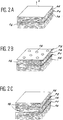
- FIGS. 2A to 2C illustrate the realization of such inclusions in a III-V matrix.
- FIG. 2A shows the matrix 14 for example in GaAs, in which a first plane P1 of inclusions 16 has been formed, for example in InAs.
- the thickness of the layers formed is counted along the X axis.
- FIG. 2B shows the formation of a second plane P2 of inclusions 16 in InAs in the matrix 14.
- FIG. 2C shows the matrix 14 in which the planes of inclusions P1 and P2 have been formed, a layer of GaAlAs having been formed on the plane of inclusions P2.
- the growth (which is carried out by molecular jets for example) is interrupted of a layer of GaAs (in the direction X) at the chosen location.
- a thin layer of InAs is then deposited on the surface of the GaAs layer.
- This InAs material has a strong mesh mismatch (around 7%) with the GaAs layer, which strongly influences its growth mode.
- Islands of InAs are formed on the surface.
- the size of these islets is fairly homogeneous, of the order of 5 nm, and the distribution of these islets on the surface of the GaAs layer is also fairly homogeneous.
- This characteristic size of 5 nm is much less than the period of the interference fringe network, which is of the order of 1 ⁇ m, and therefore allows the recording of any photorefractive network.
- the islets will be buried within this layer and will thus form inclusions.
- Such inclusions which are constrained in the GaAs matrix, do not, however, contain any dislocation and maintain good quality, which allows optimal subsequent growth conditions.
- the width of the forbidden band of InAs is less than that of the forbidden band of GaAs and the inclusions of InAs are thus attractive both for the electrons and for the holes.
- the size of the inclusions and therefore the position of the luminescence line (or of the trapping energy) depend directly on the amount of InAs deposited after the transition to three-dimensional growth mode.
- the confinement energies can range from 100 meV to 300 meV for both the electrons and the holes, which allows good lateral localization, even at room temperature and under the influence of a strong lateral electric field.
- the density of inclusions in an inclusion plane is very high (approximately 1011 cm ⁇ 2), that is to say an inclusion every 30 nm.
- the insertion of the inclusions is compatible with the subsequent growth of a good quality quantum well structure.
- This technique can be generalized to many other material systems.
- inclusions of InAs can be made in GaInAs or in InP.
- the active wells that is to say the wells where electro-absorption takes place, are in InGaAs (with approximately 10% of In), and are therefore slightly constrained, and that the inclusions of InAs be placed in a layer of AlGaAs.
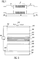
- FIG. 3 This is schematically illustrated in FIG. 3 where we see a photorefractive device according to the invention which comprises, on a substrate 18, in GaAs doped n+, a contact layer 20 in GaAs doped n+ (doping of order of 1018 cm ⁇ 3) and, on this contact layer, a layer 22 of intrinsic AlGaAs of the order of 1 ⁇ m in thickness.
- This layer 22 is surmounted by a structure 24 of quantum wells in In x Ga 1-x As, x being equal to 10%.
- Twenty wells are produced, for example, the constituent layers having a thickness of 10 nm and alternating with layers of Al y Ga 1-y As 10 nm thick, with y equal to 30%.
- an intrinsic AlGaAs layer 26 is formed on the order of 1 ⁇ m thick.
- the device On either side of the quantum well structure 24 and at about 20 nm from it, the device comprises inclusion planes 28 and 30 made up of three monolayers of InAs.
- the device comprises a contact layer 32 of pAs doped GaAs (doping of the order of 1018 cm ⁇ 3).
- the device of FIG. 3 is polarized by suitable polarization means 36 allowing reverse polarization of this device, the contact layer 32 being brought to a negative potential with respect to the contact layer 20.
- the reading wavelength changes
- the GaAs substrate is absorbent at this reading wavelength and it is then necessary either to remove the substrate by attack chemical, which is a complex process which limits the possibilities of integrating the device, ie placing the latter on a reflective layer situated between the n+ doped contact layer and the adjacent intrinsic zone.
- the barriers separating these wells can be made in AlGaAs and then use inclusions in InAs.
- the characteristic lateral displacement time is of the order of 1 ns and it is therefore necessary that the charges leave the wells corresponding to the inclusions in a comparable time.
- FIG. 4 is identical to FIG. 1 except that the thickness of the layers 38 and 40 of intrinsic material, which are respectively between the zone 10 and the inclusion plane 6 and between the zone 12 and the inclusion plane 4 , is much lower than in the case of Figure 1 to allow this tunnel effect.
- This thickness is for example of the order of 5 nm.
- the barrier height of the intrinsic material is reduced towards the outside of the inclusion planes, that is to say in the zones referenced 38 and 40, so as to promote the escape of the carriers parallel to the axis of the electric field, that is to say parallel to the axis X of FIG. 2A, with respect to their lateral displacement, that is to say perpendicular to the X axis.
- zones 38 and 40 can be made of Al x Ga 1-x As with x equal to 25%.
- quantum multi-wells alternating layers of the order of 15 nm thick and layers of the order of 10 nm thick for example, which gives a confined, quadratic Stark effect with the electric field.
- the other uses a superlattice (alternating layers of the order of 3 nm thick and layers also of the order of 3 nm thick for example), which gives a linear Wannier-Stark effect. with the electric field.
- This second configuration has the double advantage of the linearity of the electro-optical effect compared to the applied electric field and of better mobility of the carriers at the energy at which they are created.
- photocreated carriers give rise to a strong current only if they manage to escape from the wells by thermal emission or by tunnel effect, two processes which are not very effective.
- the carriers are able to undergo a tunnel effect below the energy of the barriers and can therefore be captured directly by tunnel effect in the inclusions.
- FIGS. 5 and 6 schematically illustrate the operation of a photorefractive device according to the invention.
- This device is biased in reverse, by applying an appropriate electrical voltage V between the p+-doped contact layer (area 10) of the device and the n dop-doped contact layer (area 12) of this device.
- the division into pixels can be obtained by etching the overall structure or by making localized electrical contacts.
- FIG. 7 shows an elementary pixel formed on a substrate 42 of the n+ type.
- FIG. 7 also shows a metallization layer 44 of the n+ type contact layer as well as a metallization layer 46 of the p+ type contact layer.
- an optical window should be produced on the surface of the photorefractive device as illustrated in FIG. 7 where this optical window bears the reference 48.
- these inclusions can be produced by many other techniques, one of which consists in forming a thin layer of GaAs at low temperature and then at anneal this layer to form arsenic inclusions, inclusions which, although metallic, are capable of trapping electrical charges and therefore of performing what is required for the present invention.
- the material constituting the inclusions may differ on either side of the electro-optical material.
- asymmetrical quantum wells can be produced in a similar manner to what is taught in the following document: (8) N. Susa, T. Nakahara, Appl. Phys. Lett., 60 , 2457 (1992).
- this quantum well structure in the intrinsic region of a diode pin, we can form this quantum well structure in the intrinsic zone i of a structure of type n+ / i / n+ or of a structure of type p+ / i / p+ 'by polarizing this structure for the use of the device thus obtained.
- epitaxy by molecular jets can be used but other techniques, such as for example the MOCVD technique, can be envisaged.
- the registration of a diffraction grating is done by interaction, with the device, of two laser beams Ri1 and Ri2, the whole of which constitutes the registration radiation and which are arranged symmetrically with respect to the normal to the device surface.
- the wavelength of these two beams must be such that they are absorbed efficiently by the super-structure of the device and not in the contact layers.
- a wavelength close to 900 nm is therefore used for this.
- optical power required to quickly write a network of electrical charges is of the order of 0.1 mW / cm2.
- the light beam R1 (reading radiation) which one wishes to deflect by the hologram thus recorded must have a wavelength slightly greater than that of the excitonic resonance, that is to say 960 nm.
- the optical power of this beam R1 does not matter.
Landscapes
- Physics & Mathematics (AREA)
- Chemical & Material Sciences (AREA)
- Optics & Photonics (AREA)
- Nonlinear Science (AREA)
- Engineering & Computer Science (AREA)
- Nanotechnology (AREA)
- General Physics & Mathematics (AREA)
- Life Sciences & Earth Sciences (AREA)
- Biophysics (AREA)
- Crystallography & Structural Chemistry (AREA)
- Optical Modulation, Optical Deflection, Nonlinear Optics, Optical Demodulation, Optical Logic Elements (AREA)
- Light Receiving Elements (AREA)
- Holo Graphy (AREA)
Applications Claiming Priority (2)
| Application Number | Priority Date | Filing Date | Title |
|---|---|---|---|
| FR9309784 | 1993-08-09 | ||
| FR9309784A FR2709003B1 (fr) | 1993-08-09 | 1993-08-09 | Dispositif photoréfractif à puits quantiques. |
Publications (1)
| Publication Number | Publication Date |
|---|---|
| EP0638831A1 true EP0638831A1 (de) | 1995-02-15 |
Family
ID=9450064
Family Applications (1)
| Application Number | Title | Priority Date | Filing Date |
|---|---|---|---|
| EP94401818A Withdrawn EP0638831A1 (de) | 1993-08-09 | 1994-08-05 | Quantum-Well-Photorefraktivvorrichtung |
Country Status (3)
| Country | Link |
|---|---|
| US (1) | US5559613A (de) |
| EP (1) | EP0638831A1 (de) |
| FR (1) | FR2709003B1 (de) |
Cited By (2)
| Publication number | Priority date | Publication date | Assignee | Title |
|---|---|---|---|---|
| EP0736791A1 (de) * | 1995-04-07 | 1996-10-09 | France Telecom | Photorefraktives Quantentopfbauelement |
| FR2767203A1 (fr) * | 1997-08-08 | 1999-02-12 | France Telecom | Dispositif photoretractif |
Families Citing this family (24)
| Publication number | Priority date | Publication date | Assignee | Title |
|---|---|---|---|---|
| US6025950A (en) * | 1997-09-22 | 2000-02-15 | Coretek, Inc. | Monolithic all-semiconductor optically addressed spatial light modulator based on low-photoconductive semiconductors |
| US7923260B2 (en) | 2002-08-20 | 2011-04-12 | Illumina, Inc. | Method of reading encoded particles |
| US7441703B2 (en) | 2002-08-20 | 2008-10-28 | Illumina, Inc. | Optical reader for diffraction grating-based encoded optical identification elements |
| US7619819B2 (en) | 2002-08-20 | 2009-11-17 | Illumina, Inc. | Method and apparatus for drug product tracking using encoded optical identification elements |
| WO2004019277A1 (en) * | 2002-08-20 | 2004-03-04 | Cyvera Corporation | Diffraction grating-based encoded micro-particles for multiplexed experiments |
| US7190522B2 (en) | 2002-09-12 | 2007-03-13 | Cyvera Corporation | Chemical synthesis using diffraction grating-based encoded optical elements |
| US7900836B2 (en) | 2002-08-20 | 2011-03-08 | Illumina, Inc. | Optical reader system for substrates having an optically readable code |
| US7508608B2 (en) | 2004-11-17 | 2009-03-24 | Illumina, Inc. | Lithographically fabricated holographic optical identification element |
| US7872804B2 (en) | 2002-08-20 | 2011-01-18 | Illumina, Inc. | Encoded particle having a grating with variations in the refractive index |
| US7901630B2 (en) | 2002-08-20 | 2011-03-08 | Illumina, Inc. | Diffraction grating-based encoded microparticle assay stick |
| US7164533B2 (en) | 2003-01-22 | 2007-01-16 | Cyvera Corporation | Hybrid random bead/chip based microarray |
| JP2005536769A (ja) | 2002-08-20 | 2005-12-02 | シヴェラ コーポレイション | 回折格子をベースとする光学同定要素 |
| US7399643B2 (en) | 2002-09-12 | 2008-07-15 | Cyvera Corporation | Method and apparatus for aligning microbeads in order to interrogate the same |
| US20100255603A9 (en) | 2002-09-12 | 2010-10-07 | Putnam Martin A | Method and apparatus for aligning microbeads in order to interrogate the same |
| CA2499037A1 (en) | 2002-09-12 | 2004-03-25 | Cyvera Corporation | Method and apparatus for labelling using diffraction grating-based encoded optical identification elements |
| US7092160B2 (en) * | 2002-09-12 | 2006-08-15 | Illumina, Inc. | Method of manufacturing of diffraction grating-based optical identification element |
| EP1540591A1 (de) | 2002-09-12 | 2005-06-15 | Cyvera Corporation | Mit hilfe eines beugungsgitters kodierte mikropartikeln für multiplex-experimente |
| US7433123B2 (en) | 2004-02-19 | 2008-10-07 | Illumina, Inc. | Optical identification element having non-waveguide photosensitive substrate with diffraction grating therein |
| EP2194485B1 (de) | 2004-11-16 | 2012-10-17 | Illumina, Inc. | Verfahren und Vorrichtung zum Auslesen kodierter Mikroperlen |
| US7604173B2 (en) | 2004-11-16 | 2009-10-20 | Illumina, Inc. | Holographically encoded elements for microarray and other tagging labeling applications, and method and apparatus for making and reading the same |
| WO2006055735A2 (en) | 2004-11-16 | 2006-05-26 | Illumina, Inc | Scanner having spatial light modulator |
| US7348201B2 (en) * | 2005-02-03 | 2008-03-25 | United States Of America As Represented By The Secretary Of The Army | Creation of anisotropic strain in semiconductor quantum well |
| US7623624B2 (en) | 2005-11-22 | 2009-11-24 | Illumina, Inc. | Method and apparatus for labeling using optical identification elements characterized by X-ray diffraction |
| US7830575B2 (en) | 2006-04-10 | 2010-11-09 | Illumina, Inc. | Optical scanner with improved scan time |
Citations (1)
| Publication number | Priority date | Publication date | Assignee | Title |
|---|---|---|---|---|
| WO1992022847A1 (fr) * | 1991-06-19 | 1992-12-23 | France Telecom | Dispositif photorefractif |
Family Cites Families (5)
| Publication number | Priority date | Publication date | Assignee | Title |
|---|---|---|---|---|
| US5004325A (en) * | 1990-01-16 | 1991-04-02 | At&T Bell Laboratories | Optical processing using a multilayer heterostructure |
| US5315430A (en) * | 1992-04-15 | 1994-05-24 | The United States Of America As Represented By The United States Department Of Energy | Strained layer Fabry-Perot device |
| US5345328A (en) * | 1992-08-12 | 1994-09-06 | Sandia Corporation | Tandem resonator reflectance modulator |
| US5323019A (en) * | 1993-04-20 | 1994-06-21 | The United States Of America As Represented By The Secretary Of The Army | All optical multiple quantum well optical modulator |
| US5381260A (en) * | 1993-11-19 | 1995-01-10 | The United States Of America As Represented By The Secretary Of The Army | Uniaxially strained semiconductor multiple quantum well device using direction-dependent thermal expansion coefficients in a host substrate |
-
1993
- 1993-08-09 FR FR9309784A patent/FR2709003B1/fr not_active Expired - Fee Related
-
1994
- 1994-08-05 EP EP94401818A patent/EP0638831A1/de not_active Withdrawn
- 1994-08-05 US US08/286,703 patent/US5559613A/en not_active Expired - Fee Related
Patent Citations (1)
| Publication number | Priority date | Publication date | Assignee | Title |
|---|---|---|---|---|
| WO1992022847A1 (fr) * | 1991-06-19 | 1992-12-23 | France Telecom | Dispositif photorefractif |
Non-Patent Citations (4)
| Title |
|---|
| GOLDSTEIN L ET AL: "Growth by molecular beam epitaxy and characterization of InAs/GaAs strained-layer superlattices", APPLIED PHYSICS LETTERS., vol. 47, no. 10, November 1985 (1985-11-01), NEW YORK US, pages 1099 - 1101 * |
| NOLTE D D ET AL: "Resonant photodiffractive effect in semi-insulating multiple quantum wells", JOURNAL OF THE OPTICAL SOCIETY OF AMERICA - B, vol. 7, no. 11, November 1990 (1990-11-01), NEW YORK US, pages 2217 - 2225, XP000162466 * |
| PARTOVI A ET AL: "High sensitivity optical image processing device based on CdZnTe/ZnTe multiple quantum well structures", APPLIED PHYSICS LETTERS., vol. 59, no. 7000, October 1991 (1991-10-01), NEW YORK US, pages 1832 - 1834, XP000265117 * |
| PARTOVI A ET AL: "High-speed photodiffractive effect in semi-insulating CdZnTe/ZnTe multiple quantum wells", OPTICS LETTERS., vol. 17, no. 9, May 1992 (1992-05-01), NEW YORK US, pages 655 - 657, XP000461102 * |
Cited By (3)
| Publication number | Priority date | Publication date | Assignee | Title |
|---|---|---|---|---|
| EP0736791A1 (de) * | 1995-04-07 | 1996-10-09 | France Telecom | Photorefraktives Quantentopfbauelement |
| FR2732782A1 (fr) * | 1995-04-07 | 1996-10-11 | Lambert Bertrand | Dispositif photoreactif perfectionne |
| FR2767203A1 (fr) * | 1997-08-08 | 1999-02-12 | France Telecom | Dispositif photoretractif |
Also Published As
| Publication number | Publication date |
|---|---|
| US5559613A (en) | 1996-09-24 |
| FR2709003A1 (fr) | 1995-02-17 |
| FR2709003B1 (fr) | 1995-09-15 |
Similar Documents
| Publication | Publication Date | Title |
|---|---|---|
| EP0638831A1 (de) | Quantum-Well-Photorefraktivvorrichtung | |
| US7701629B2 (en) | Photonic device including semiconductor structure having doped region with array of subwavelengh recesses | |
| EP0575227B1 (de) | Verfahren und Vorrichtung zur Modulation und Verstärkung von Lichtstrahlen | |
| US5508829A (en) | LTG AlGaAs non-linear optical material and devices fabricated therefrom | |
| FR2495383A1 (fr) | Diode electroluminescente a superradiance ayant un rendement de couplage eleve avec un guide d'ondes optiques | |
| EP1067643A1 (de) | Optische Halbleitervorrichtung mit einem wellenlängenabstimmbarem Resonanzhohlraum, und Anwendung in Lichtintensitätsmodulation | |
| FR2681191A1 (fr) | Composant integre laser-modulateur a super-reseau tres couple. | |
| CA1314615C (fr) | Modulateur d'onde electromagnetique a puits quantiques couples, et application a un detecteur d'onde electromagnetique | |
| WO1992022847A1 (fr) | Dispositif photorefractif | |
| FR2729789A1 (fr) | Detecteur a puits quantique et procede de realisation | |
| EP0306400B1 (de) | Quantum-well-Modulator für elektromagnetische Wellen und Anwendung dieses Modulators als Polarisator | |
| EP0436413B1 (de) | Verfahren und Vorrichtung zur elektrooptischen Modulation unter Benutzung des niederenergetischen schrägen Überganges in einem stark gekoppelten Übergitter | |
| EP0664588B1 (de) | Halbleiterstruktur mit virtuellem Beugungsgitter | |
| US5229878A (en) | Method and apparatus for modulating light using semiconductor element having quantum well structure | |
| CA2769478A1 (fr) | Dispositifs electro-optiques bases sur la variation d'indice ou d'absorption dans des transitions isb | |
| FR2719417A1 (fr) | Composant à hétérostructure semi-conductrice, commande par la lumière pour la génération d'oscillations hyperfréquences. | |
| FR2855653A1 (fr) | Structure amorphe de couplage optique pour detecteur d'ondes electromagnetiques et detecteur associe | |
| EP0736791B1 (de) | Photorefraktives Quantentopfbauelement | |
| EP0658791A1 (de) | Lichtbrechende Zelle | |
| EP0658792A1 (de) | Optischer Prozessor mit Quantumwell-Heterostruktur | |
| WO2020193786A9 (fr) | Modulateur ultra-rapide de l'amplitude d'un rayonnement laser | |
| EP4237907B1 (de) | Vorrichtung zur erzeugung einzelner photonen und verschränkter photonenpaare | |
| Trezza et al. | Creation and optimization of vertical-cavity X-modulators | |
| EP0545787B1 (de) | Halbleiterheterostruktur für die Verarbeitung eines optischen Signals | |
| EP0640866B1 (de) | Reine optische bistabile Vorrichtung vom "SEED"-Typ |
Legal Events
| Date | Code | Title | Description |
|---|---|---|---|
| PUAI | Public reference made under article 153(3) epc to a published international application that has entered the european phase |
Free format text: ORIGINAL CODE: 0009012 |
|
| AK | Designated contracting states |
Kind code of ref document: A1 Designated state(s): DE GB IT |
|
| 17P | Request for examination filed |
Effective date: 19950722 |
|
| STAA | Information on the status of an ep patent application or granted ep patent |
Free format text: STATUS: THE APPLICATION IS DEEMED TO BE WITHDRAWN |
|
| 18D | Application deemed to be withdrawn |
Effective date: 19980303 |