EP0545787B1 - Halbleiterheterostruktur für die Verarbeitung eines optischen Signals - Google Patents
Halbleiterheterostruktur für die Verarbeitung eines optischen Signals Download PDFInfo
- Publication number
- EP0545787B1 EP0545787B1 EP92403193A EP92403193A EP0545787B1 EP 0545787 B1 EP0545787 B1 EP 0545787B1 EP 92403193 A EP92403193 A EP 92403193A EP 92403193 A EP92403193 A EP 92403193A EP 0545787 B1 EP0545787 B1 EP 0545787B1
- Authority
- EP
- European Patent Office
- Prior art keywords
- thin film
- well
- heterostructure
- band
- equal
- Prior art date
- Legal status (The legal status is an assumption and is not a legal conclusion. Google has not performed a legal analysis and makes no representation as to the accuracy of the status listed.)
- Expired - Lifetime
Links
Images




Classifications
-
- B—PERFORMING OPERATIONS; TRANSPORTING
- B82—NANOTECHNOLOGY
- B82Y—SPECIFIC USES OR APPLICATIONS OF NANOSTRUCTURES; MEASUREMENT OR ANALYSIS OF NANOSTRUCTURES; MANUFACTURE OR TREATMENT OF NANOSTRUCTURES
- B82Y20/00—Nanooptics, e.g. quantum optics or photonic crystals
-
- G—PHYSICS
- G02—OPTICS
- G02F—OPTICAL DEVICES OR ARRANGEMENTS FOR THE CONTROL OF LIGHT BY MODIFICATION OF THE OPTICAL PROPERTIES OF THE MEDIA OF THE ELEMENTS INVOLVED THEREIN; NON-LINEAR OPTICS; FREQUENCY-CHANGING OF LIGHT; OPTICAL LOGIC ELEMENTS; OPTICAL ANALOGUE/DIGITAL CONVERTERS
- G02F1/00—Devices or arrangements for the control of the intensity, colour, phase, polarisation or direction of light arriving from an independent light source, e.g. switching, gating or modulating; Non-linear optics
- G02F1/01—Devices or arrangements for the control of the intensity, colour, phase, polarisation or direction of light arriving from an independent light source, e.g. switching, gating or modulating; Non-linear optics for the control of the intensity, phase, polarisation or colour
- G02F1/015—Devices or arrangements for the control of the intensity, colour, phase, polarisation or direction of light arriving from an independent light source, e.g. switching, gating or modulating; Non-linear optics for the control of the intensity, phase, polarisation or colour based on semiconductor elements having potential barriers, e.g. having a PN or PIN junction
- G02F1/017—Structures with periodic or quasi periodic potential variation, e.g. superlattices, quantum wells
- G02F1/01725—Non-rectangular quantum well structures, e.g. graded or stepped quantum wells
-
- H—ELECTRICITY
- H10—SEMICONDUCTOR DEVICES; ELECTRIC SOLID-STATE DEVICES NOT OTHERWISE PROVIDED FOR
- H10F—INORGANIC SEMICONDUCTOR DEVICES SENSITIVE TO INFRARED RADIATION, LIGHT, ELECTROMAGNETIC RADIATION OF SHORTER WAVELENGTH OR CORPUSCULAR RADIATION
- H10F77/00—Constructional details of devices covered by this subclass
- H10F77/10—Semiconductor bodies
- H10F77/14—Shape of semiconductor bodies; Shapes, relative sizes or dispositions of semiconductor regions within semiconductor bodies
-
- G—PHYSICS
- G02—OPTICS
- G02F—OPTICAL DEVICES OR ARRANGEMENTS FOR THE CONTROL OF LIGHT BY MODIFICATION OF THE OPTICAL PROPERTIES OF THE MEDIA OF THE ELEMENTS INVOLVED THEREIN; NON-LINEAR OPTICS; FREQUENCY-CHANGING OF LIGHT; OPTICAL LOGIC ELEMENTS; OPTICAL ANALOGUE/DIGITAL CONVERTERS
- G02F1/00—Devices or arrangements for the control of the intensity, colour, phase, polarisation or direction of light arriving from an independent light source, e.g. switching, gating or modulating; Non-linear optics
- G02F1/01—Devices or arrangements for the control of the intensity, colour, phase, polarisation or direction of light arriving from an independent light source, e.g. switching, gating or modulating; Non-linear optics for the control of the intensity, phase, polarisation or colour
- G02F1/015—Devices or arrangements for the control of the intensity, colour, phase, polarisation or direction of light arriving from an independent light source, e.g. switching, gating or modulating; Non-linear optics for the control of the intensity, phase, polarisation or colour based on semiconductor elements having potential barriers, e.g. having a PN or PIN junction
- G02F1/017—Structures with periodic or quasi periodic potential variation, e.g. superlattices, quantum wells
- G02F1/01775—Structures with periodic or quasi periodic potential variation, e.g. superlattices, quantum wells involving an inter-subband transition in one well, e.g. e1->e2
-
- G—PHYSICS
- G02—OPTICS
- G02F—OPTICAL DEVICES OR ARRANGEMENTS FOR THE CONTROL OF LIGHT BY MODIFICATION OF THE OPTICAL PROPERTIES OF THE MEDIA OF THE ELEMENTS INVOLVED THEREIN; NON-LINEAR OPTICS; FREQUENCY-CHANGING OF LIGHT; OPTICAL LOGIC ELEMENTS; OPTICAL ANALOGUE/DIGITAL CONVERTERS
- G02F1/00—Devices or arrangements for the control of the intensity, colour, phase, polarisation or direction of light arriving from an independent light source, e.g. switching, gating or modulating; Non-linear optics
- G02F1/35—Non-linear optics
- G02F1/355—Non-linear optics characterised by the materials used
- G02F1/3556—Semiconductor materials, e.g. quantum wells
Definitions
- the present invention relates to a semiconductor heterostructure which allows efficient intra-band absorption of electromagnetic radiation whose wavelength is less than or equal to 3 micrometers.
- a heterostructure according to the present invention is capable of absorbing in a narrow spectral window which is centered on a given wavelength, less than or equal to 3 micrometers.
- the heterostructure which is the subject of the invention can constitute the active medium of a detector, a modulator or a stop-band filter operating at wavelengths less than or equal to 3 micrometers, these wavelengths being for example between 1.5 micrometer and 3 micrometers.
- the invention therefore has applications in optoelectronics and in particular in the field of telecommunications by optical fibers.
- This mechanism is operated by a family of semiconductor components (detectors, modulators) which work mainly in the far infrared (wavelengths of the order of 10 micrometers).
- the minimum operating wavelength is of the order of 3.5 micrometers.
- the present invention provides a semiconductor heterostructure which greatly increases the effective operating range of devices using intra-band absorption.
- part A it is recalled that a quantum well is obtained by the insertion of a thin layer 2 of a semiconductor material between two semiconductor layers 4 whose forbidden band has a width greater than that of layer 2, these layers 4 being called "barrier layers".
- materials from the same semiconductor family (III-V, II-VI or IV) are used to make layers 2 and 4.
- Quantum mechanics teaches that the electronic conduction states of such a structure come together, due to the confinement of the following electrons z, in several sub-bands which are almost parallel.
- the first two sub-bands are respectively denoted SB1 and SB2 and the energies of the minima of the sub-bands SB1 and SB2 are respectively denoted E1 and E2, with E2 greater than E1.
- FIG. 2 shows the dispersion curves of the sub-bands SB1 and SB2, E representing the energy and k // representing the modulus of the wave vector of an electron in the plane (x, y) .
- the conduction states are then populated up to a certain energy EF (Fermi level), the upper states remaining almost empty.
- EF Fermi level
- FIG. 2 This is illustrated by FIG. 2 where the reference ep designates the populated conduction states and the reference ev designates the empty conduction states.
- Intra-band absorption also called inter-sub-band absorption
- the absorption peak has a finite width of the order of 6 to 7 meV, which reflects the short life time (phase shift time) of the electron in its arrival state after absorption.
- the total absorption associated with the transition from SB1 to SBj, integrated over the entire resonance line is proportional, for a given configuration of excitation (angle of incidence and polarization of the electromagnetic radiation ) the product of the force of oscillators f1j by the density of carriers in the well, this density usually being between 10 11 and 10 12 carriers per cm 2 .
- quantum multi-wells are produced, in which the absorbent structure is repeated fifty times to increase the absorption coefficient of the structure while retaining a reasonable thickness for it.
- the present invention aims to extend towards the short wavelengths the operating range of these devices and, to do this, to extend the energy range in which it is possible to obtain efficient intra-band absorption.
- Document (4) shows the interest of quantum wells for frequency doubling in medium infrared (5 to 20 micrometers).
- a first approach consists in reducing the width a of the well and a second approach consists in using transitions between SB1 and SBn, with n greater than 2.
- the present invention relates to a semiconductor heterostructure which does not have these drawbacks.
- the invention makes it possible to increase the spacing between the sub-bands SB1 and SB2 of a quantum well, and therefore the energy of the intra-band transition, while increasing the oscillator strength of this transition.
- the subject of the present invention is a semiconductor heterostructure according to claim 1.
- the constituent materials of the thin layer and of the layers between which this thin layer is found may belong to the same family of semiconductor materials.
- the thin layer is made of Ga 1-x Al x As and the layers between which this thin layer is found are made of Ga 1- y Al y As, x being positive or zero and less than y, y being less than or equal to 1.
- the ultrafine layer can be In z Ga 1-z As, z being greater than 0 and less than or equal to 1.
- the thin layer is made of Ga 1-x Al x Sb and the layers between which this thin layer is located are made of Ga y Al 1-y Sb, x being positive or zero and less than y, y being less than or equal to 1.
- the ultrafine layer may be made of InAs.
- the heterostructure object of the invention can be doped by donors, so as to populate with electrons the bottom of the sub-band whose minimum energy is E1.
- heterostructure which is the subject of the invention may comprise several stacked copies of said motif, in order to form a quantum multiwell structure.
- the first approach consists in reducing the width a of the well (see fig. 1) in order to increase the distance between SB1 and SB2.
- the energies E1 and E2 are inversely proportional to the square of a when the height Vb of the potential barrier (depth of the well) is much greater than the energy E2.
- the oscillator strength f12 of the transition from SB1 to SB2 remains constant when a decreases.
- E2 is at least 750 meV from the bottom of the well.
- Vb conduction band discontinuity
- E2 conduction band discontinuity
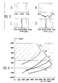
- FIGS. 3 to 6 summarize the interdependence of the well parameters (width, intra-band transition energy, position of E1, oscillator force f12 from SB1 to SB2) for various structures A, B , C and D ( Figure 3).
- FIG. 7B shows the wave functions of the first electron states of the structure for a well GaAs narrow.
- Electrons in the X valley are subjected to a potential well in the AlAs layers.
- the first type X levels of the structure have an energy close to 180 meV compared to the bottom of the well.
- the first electronic level of conduction of the structure is the first level of the family X and not the level E1 of the structure (see fig. 7B) .
- the barriers are made of AlAs and the well consists of a layer of GaAs (structure A), of In 0.2 Ga 0.8 As (structure B), of a GaAs layer with two monolayers of InAs in the middle (structure C according to the invention) or a GaAs layer with three monolayers of InAs in the middle (structure D according to the invention).
- E2-E1 is given as a function of the width a of the well, the bold lines corresponding to the range of possible use of these quantum wells.
- the oscillator strength f12 of the intra-band transition is given as a function of E2-E1, the bold lines corresponding to the range of possible use of these quantum wells.
- the maximum value reached is around 600 meV (see Figure 5, structure (A)).
- the electronic properties are then very sensitive to the quality of the structure and to the perfection of the interfaces in particular.
- This material has a lattice parameter different from GaAs but can however be deposited in a constrained thin layer on GaAs.
- the first problem (position with respect to X1) is alleviated by the overall displacement of the levels of the well.
- Transition energies of the order of 600 meV are a priori thus accessible.
- the third problem is not alleviated: in the range of accessible transition energies, the dependence of E2-E1 as a function of the width of the well is almost identical for a well of GaAs or of In 0.2 Ga 0 , 8 As (in both cases, AlAs acts as an infinite height barrier).
- GaSb has a bandgap energy of 0.75 eV at low temperature, which makes it an interesting material for optoelectronics.
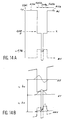
- FIG. 14A The configuration of bands for GaSb, AlSb (and InAs materials used in heterostructures according to the invention) is presented in FIG. 14A where BV and BC represent the valence band and the conduction band respectively.
- the in-band transition energy can be at most 150 to 200 meV: indeed, the minimum of the L band of AlSb is placed 80 meV above the minimum gamma of GaSb.
- the energy difference E2-E1 saturates at 0.6 eV and then decreases for a well width less than 2.8 nm.
- the well is constituted by a layer of GaAs and a layer of alloy Ga x Al 1-x As (0 ⁇ x ⁇ 1), placed between barrier layers of AlAs.
- Figure 9 shows the variations of the oscillator force f13 as a function of the energy of transition E3-E1 as well as the accessible domain II (the hatched domain I is inaccessible) using this type of well for the GaAs / AlAs system.
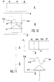
- FIG. 10 shows, in its part A, a known semiconductor heterostructure, of the kind of that of FIG. 1 and comprising a well layer 6 between two barrier layers 8 to form a quantum well.
- Part B of FIG. 10 shows the wave function of the states of the first two corresponding sub-bands, the minimum energies of which are denoted E1 and E2 respectively.
- Figure 11 relates to a heterostructure according to the invention.
- the invention is in fact based on a observation mentioned in document (6) that the substitution of an ultrafine layer of the quantum well material by a semiconductor material of the same family (III-V or II-VI for example) can significantly and selectively modify , the energy positions of the different sub-bands.
- the heterostructure according to the invention represented in part A of FIG. 11, comprises a well layer comprised between two barrier layers as well as an ultrathin S layer (composed of a few monolayers), attractive and inserted in the center of the well obtained.
- the barrier layers bear the reference 12 and the well layer, in which the layer S is inserted, is therefore in two parts bearing the references 10a and 10b respectively.
- a monolayer has a thickness of the order of 0.3 nm.
- Part B of FIG. 11 shows the new potential profile of the well thus obtained.
- An electron in the SB1 sub-band has a high density of probability of presence at the center of the quantum well.
- GaAs / AlAs systems i.e. Ga 1-x Al x As for the well layer and Ga 1-y Al y As for the layers -barriers, with x positive or zero and less than y and y less than or equal to 1
- GaSb / AlSb i.e. Ga 1-x Al x Sb for the well layer and Ga y Al 1- y Sb for the barrier layers, with x positive or zero and less than y and y less than or equal to 1).
- GaAs / AlAs system for example InAs (or more precisely In z Ga 1-z As with z positive and less than or equal to 1) is used to produce the layer S which disturbs the GaAs / AlAs structure.
- InAs or more precisely In z Ga 1-z As with z positive and less than or equal to 1 is used to produce the layer S which disturbs the GaAs / AlAs structure.
- InAs is a material with a smaller prohibited band than GaAs and makes it possible to generate an attractive disturbance in the latter.
- a very thin layer of InAs comprising two monolayers which are deposited on GaAs by a conventional growth technique (EJM or OMCVD).
- Intra-band absorption at energies exceeding 0.8 eV is made possible.
- the width of the well is greater in the case of the modified structure.
- the layer S For the structures used under electric field, one could prefer to place the layer S at the node of the wave function of the second level (in order to move this one as little as possible) or to the maximum of density of propability of presence of the first level (to lower it as much as possible).
- This displacement can be compensated by an offset from the nominal position of the InAs plane.
- This one has a strong attractive character for the electrons because the discontinuity of bands in the vicinity of the interface InAs / GaSb is worth 1 eV.
- FIG. 14A the configuration of bands for the InAs, GaSb and AlSb materials is shown in FIG. 14A.
- n monolayers (n greater than or equal to 2 and less than or equal to 6) of GaSb by InAs at the center of the well makes it possible to greatly increase the range of transition energies accessible in this system, as shown in FIGS. 12 and 13 in which the bold lines correspond to the range of possible use of the quantum wells.
- a is the width of a well (thickness of GaSb plus thickness of the n MC monolayers of InAs).
- An advantage of this system compared to the InAs / GaAs / AlAs system is that a desired value E2-E1 can be obtained here starting from a larger well which is therefore more easily achievable and less susceptible to imperfections.
- n for n greater than or equal to 4, is an overall displacement of the levels E1 and E2 towards low energies and a corresponding reduction in the bandgap energy of the structure.
- a second advantage of this system is therefore that the intra-band transition energy (very sensitive to the width of the well) and the band gap energy can be adjusted relatively independently if necessary.
- InSb two or three monolayers
- InSb In
- a component uses intra-band absorption, it is therefore possible to extend its operating range towards short wavelengths by modifying only, in accordance with the invention, the well (or the wells in the case of a quantum multi-well structure) where intra-band absorption occurs.
- the in-band transition energy and the energy E 1 -HH 1 of the band gap of the structure are simultaneously very close to 0.8 eV.
- the second harmonic generation coefficient is proportional to: ⁇ t ⁇ 2> ⁇ 2 z ⁇ 1> ⁇ 1 ⁇ t> (E2-Et-2hv) (E1-Et-hv)
- the interband (in the order of 0.79 eV) and inband (in the order of 0.81 eV) transition energies are simultaneously close to the resonance at 0.8 eV.
- ⁇ 2> are large (they are worth 0.63 and 0.42 respectively) and the oscillator strength of the in-band transition (linked to the matrix element ⁇ 1
- an undoped version of the structure of the invention can constitute the active medium of an all-optical modulator, working at 1.55 micrometer and controlled by radiation of the same wavelength.
Landscapes
- Physics & Mathematics (AREA)
- Nonlinear Science (AREA)
- Optics & Photonics (AREA)
- Chemical & Material Sciences (AREA)
- Engineering & Computer Science (AREA)
- Nanotechnology (AREA)
- General Physics & Mathematics (AREA)
- Life Sciences & Earth Sciences (AREA)
- Biophysics (AREA)
- Crystallography & Structural Chemistry (AREA)
- Recrystallisation Techniques (AREA)
Claims (8)
- Halbleiterheterostruktur für die Verarbeitung eines optischen Signals mit mindestens einem Grundelement, das eine dünne Schicht (10a,10b) aus einem Halbleitermaterial und zwei Halbleitersperrschichten (12) umfaßt, zwischen denen sich die dünne Schicht befindet und die eine größere Breite eines verbotenen Bandes aufweisen als die dünne Schicht, wodurch eine Potentialsenke geschaffen wird, wobei die Heterostruktur weiterhin eine ultrafeine anziehende Schicht (S) umfaßt, die aus mehreren Monoschichten zusammengesetzt ist, die in der dünnen Schicht ungefähr in der Mitte von dieser eingefügt ist, und die aus einem Halbleitermaterial gefertigt ist, das der selben Familie angehört wie das Material der dünnen Schicht (10a,10b), und eine Breite eines verbotenen Bandes aufweist, die kleiner als die der dünnen Schicht ist, wobei die Heterostruktur dadurch gekennzeichnet ist, daß
sie mindestens zwei Unterbänder aufweist, deren minimale Energiezustände in der Potentialsenke enthalten sind und deren minimale Energie bezeichnet sind mit E1 bzw. E2, wobei E2 größer ist als E1, wobei die Tiefe der Potentialsenke weit über der von E2 liegt und der Abstand zwischen den Energieminima dieser Unterbanden mindestens gleich 400 meV ist, so- daß sie die Intrabandenabsorption von entsprechenden Energiestrahlen erlaubt, wobei das Unterband, dessen minimale Energie gleich E1 entspricht, geeignet ist, besetzt zu werden. - Heterostruktur nach Anspruch 1, dadurch gekennzeichnet, daß die Materialien, die die dünne Schicht (10a,10b) und die Schichten (12) bilden, zwischen welchen sich diese dünne Schicht befindet, zur selben Familie von Halbleitermaterialien gehören.
- Heterostruktur nach Anspruch 2, dadurch gekennzeichnet, daß die dünne Schicht (10a,10b) aus Ga1-xAlxAs besteht, und die Schichten (12), zwischen welchen sich diese dünne Schicht befindet, aus Ga1-yAlyAs besteht, wobei x positif oder Null und kleiner als y ist, und y kleiner oder gleich 1 ist.
- Heterostruktur nach Anspruch 3, dadurch gekennzeichnet, daß die ultrafeine Schicht (S) aus InzGa1-zAs besteht, wobei z größer als 0 und kleiner oder gleich 1 ist.
- Heterostruktur nach Anspruch 2, dadurch gekennzeichnet, daß die dünne Schicht (10a,10b) aus Ga1-xAlxSb besteht, und die Schichten (12), zwischen welchen sich diese dünne Schicht befindet, aus GayAl1-ySb besteht, wobei x positif oder Null und kleiner als y ist, und y kleiner oder gleich 1 ist.
- Heterostruktur nach Anspruch 5, dadurch gekennzeichnet, daß die ultrafeine Schicht (S) aus InAs besteht.
- Heterostruktur nach einem der Ansprüche 1 - 6, dadurch gekennzeichnet, daß sie mit Donatoren derart dotiert ist, daß der Boden des Unterbandes, dessen Energie gleich E1 ist, von Elektronen bevölkert ist.
- Heterostruktur dadurch gekennzeichnet, daß sie eine Aufeinanderschichtung von mehreren Heterostrukturen gemäß einem der Ansprüche 1 bis 7 umfaßt.
Applications Claiming Priority (2)
| Application Number | Priority Date | Filing Date | Title |
|---|---|---|---|
| FR9114831 | 1991-11-29 | ||
| FR9114831A FR2684489B1 (fr) | 1991-11-29 | 1991-11-29 | Heterostructure semiconductrice pour le traitement d'un signal optique. |
Publications (2)
| Publication Number | Publication Date |
|---|---|
| EP0545787A1 EP0545787A1 (de) | 1993-06-09 |
| EP0545787B1 true EP0545787B1 (de) | 1997-08-20 |
Family
ID=9419523
Family Applications (1)
| Application Number | Title | Priority Date | Filing Date |
|---|---|---|---|
| EP92403193A Expired - Lifetime EP0545787B1 (de) | 1991-11-29 | 1992-11-26 | Halbleiterheterostruktur für die Verarbeitung eines optischen Signals |
Country Status (3)
| Country | Link |
|---|---|
| EP (1) | EP0545787B1 (de) |
| DE (1) | DE69221704T2 (de) |
| FR (1) | FR2684489B1 (de) |
Families Citing this family (1)
| Publication number | Priority date | Publication date | Assignee | Title |
|---|---|---|---|---|
| FR2693594B1 (fr) * | 1992-07-07 | 1994-08-26 | Thomson Csf | Détecteur d'ondes électromagnétiques à puits quantiques. |
-
1991
- 1991-11-29 FR FR9114831A patent/FR2684489B1/fr not_active Expired - Lifetime
-
1992
- 1992-11-26 DE DE69221704T patent/DE69221704T2/de not_active Expired - Lifetime
- 1992-11-26 EP EP92403193A patent/EP0545787B1/de not_active Expired - Lifetime
Also Published As
| Publication number | Publication date |
|---|---|
| FR2684489A1 (fr) | 1993-06-04 |
| DE69221704T2 (de) | 1998-01-22 |
| DE69221704D1 (de) | 1997-09-25 |
| FR2684489B1 (fr) | 1998-08-14 |
| EP0545787A1 (de) | 1993-06-09 |
Similar Documents
| Publication | Publication Date | Title |
|---|---|---|
| EP0575227B1 (de) | Verfahren und Vorrichtung zur Modulation und Verstärkung von Lichtstrahlen | |
| EP0432035A1 (de) | Optische Quantumwell-Vorrichtung und Herstellungsverfahren | |
| EP0638831A1 (de) | Quantum-Well-Photorefraktivvorrichtung | |
| EP0551030A1 (de) | Quantentopf-Transistor mit resonantem Tunneleffekt | |
| WO1993015525A1 (fr) | Detecteur infrarouge a puits quantiques | |
| WO2020169503A1 (fr) | Amplificateur paramétrique à onde progressive à basse impédance caractéristique et son procédé de fabrication | |
| EP0306400B1 (de) | Quantum-well-Modulator für elektromagnetische Wellen und Anwendung dieses Modulators als Polarisator | |
| EP0436413B1 (de) | Verfahren und Vorrichtung zur elektrooptischen Modulation unter Benutzung des niederenergetischen schrägen Überganges in einem stark gekoppelten Übergitter | |
| EP0522952A2 (de) | Feldeffekt-Transistor mit dünnen Barrierenschichten und einer dünnen, dotierten Schicht | |
| EP0545787B1 (de) | Halbleiterheterostruktur für die Verarbeitung eines optischen Signals | |
| EP0557141A1 (de) | Optischer Frequenzverdoppler mit Halbleiter-Quantumstrukturen | |
| EP0557186B1 (de) | Photoelektrischer Detektor mit Quantentöpfen und verbesserter Detectivität | |
| WO2011012833A2 (fr) | Dispositifs electro-optiques bases sur la variation d'indice ou d'absorption dans des transitions isb | |
| EP3948409B1 (de) | Ultraschneller modulator zur modulation der amplitude von laserstrahlung | |
| EP0274289B1 (de) | Optischer Übergitter-Modulator | |
| EP0736791B1 (de) | Photorefraktives Quantentopfbauelement | |
| EP3948407B1 (de) | Zur unterstützung von tamm-modi fähiger elektromagnetischer hohlraum | |
| EP0477072B1 (de) | Mehrschichtiger elektrooptischer Lichtmodulator | |
| EP0640866B1 (de) | Reine optische bistabile Vorrichtung vom "SEED"-Typ | |
| EP0554178B1 (de) | Optischer Halbleiterverstärker mit kurzer Schaltzeit | |
| FR2723485A1 (fr) | Modulateur a effet stark de confinement quantique insensible a la polarisation | |
| FR2933542A1 (fr) | Dispositif a cascades quantiques a injecteur haut | |
| WO2021089687A1 (fr) | Laser à verrouillage de mode à tranchées et composant optique associé | |
| EP0880047A1 (de) | Optischer Filter mit einer Multiquantentopfstruktur | |
| EP0658791A1 (de) | Lichtbrechende Zelle |
Legal Events
| Date | Code | Title | Description |
|---|---|---|---|
| PUAI | Public reference made under article 153(3) epc to a published international application that has entered the european phase |
Free format text: ORIGINAL CODE: 0009012 |
|
| AK | Designated contracting states |
Kind code of ref document: A1 Designated state(s): DE GB |
|
| 17P | Request for examination filed |
Effective date: 19931118 |
|
| 17Q | First examination report despatched |
Effective date: 19941214 |
|
| GRAG | Despatch of communication of intention to grant |
Free format text: ORIGINAL CODE: EPIDOS AGRA |
|
| GRAH | Despatch of communication of intention to grant a patent |
Free format text: ORIGINAL CODE: EPIDOS IGRA |
|
| GRAH | Despatch of communication of intention to grant a patent |
Free format text: ORIGINAL CODE: EPIDOS IGRA |
|
| GRAA | (expected) grant |
Free format text: ORIGINAL CODE: 0009210 |
|
| AK | Designated contracting states |
Kind code of ref document: B1 Designated state(s): DE GB |
|
| REF | Corresponds to: |
Ref document number: 69221704 Country of ref document: DE Date of ref document: 19970925 |
|
| GBT | Gb: translation of ep patent filed (gb section 77(6)(a)/1977) |
Effective date: 19971024 |
|
| PLBE | No opposition filed within time limit |
Free format text: ORIGINAL CODE: 0009261 |
|
| STAA | Information on the status of an ep patent application or granted ep patent |
Free format text: STATUS: NO OPPOSITION FILED WITHIN TIME LIMIT |
|
| 26N | No opposition filed | ||
| REG | Reference to a national code |
Ref country code: GB Ref legal event code: IF02 |
|
| REG | Reference to a national code |
Ref country code: GB Ref legal event code: 732E |
|
| REG | Reference to a national code |
Ref country code: GB Ref legal event code: 732E |
|
| PGFP | Annual fee paid to national office [announced via postgrant information from national office to epo] |
Ref country code: DE Payment date: 20101124 Year of fee payment: 19 |
|
| PGFP | Annual fee paid to national office [announced via postgrant information from national office to epo] |
Ref country code: GB Payment date: 20101124 Year of fee payment: 19 |
|
| REG | Reference to a national code |
Ref country code: DE Ref legal event code: R071 Ref document number: 69221704 Country of ref document: DE |
|
| REG | Reference to a national code |
Ref country code: GB Ref legal event code: PE20 Expiry date: 20121125 |
|
| PG25 | Lapsed in a contracting state [announced via postgrant information from national office to epo] |
Ref country code: GB Free format text: LAPSE BECAUSE OF EXPIRATION OF PROTECTION Effective date: 20121125 |