EP0638996A1 - Chopper-Differenzverstärker mit MOS-Kondensatoren - Google Patents
Chopper-Differenzverstärker mit MOS-Kondensatoren Download PDFInfo
- Publication number
- EP0638996A1 EP0638996A1 EP94112234A EP94112234A EP0638996A1 EP 0638996 A1 EP0638996 A1 EP 0638996A1 EP 94112234 A EP94112234 A EP 94112234A EP 94112234 A EP94112234 A EP 94112234A EP 0638996 A1 EP0638996 A1 EP 0638996A1
- Authority
- EP
- European Patent Office
- Prior art keywords
- differential amplifier
- input
- precharging
- voltage
- input end
- Prior art date
- Legal status (The legal status is an assumption and is not a legal conclusion. Google has not performed a legal analysis and makes no representation as to the accuracy of the status listed.)
- Granted
Links
- 239000003990 capacitor Substances 0.000 title claims abstract description 54
- 238000005070 sampling Methods 0.000 claims description 32
- 230000004044 response Effects 0.000 claims description 3
- 238000010586 diagram Methods 0.000 description 9
- XUIMIQQOPSSXEZ-UHFFFAOYSA-N Silicon Chemical compound [Si] XUIMIQQOPSSXEZ-UHFFFAOYSA-N 0.000 description 5
- 229910052710 silicon Inorganic materials 0.000 description 5
- 239000010703 silicon Substances 0.000 description 5
- 230000008859 change Effects 0.000 description 3
- 239000013078 crystal Substances 0.000 description 3
- 230000007257 malfunction Effects 0.000 description 3
- 239000012535 impurity Substances 0.000 description 2
- 230000004048 modification Effects 0.000 description 2
- 238000012986 modification Methods 0.000 description 2
- 230000014509 gene expression Effects 0.000 description 1
- 238000002347 injection Methods 0.000 description 1
- 239000007924 injection Substances 0.000 description 1
- 238000004519 manufacturing process Methods 0.000 description 1
- 239000000758 substrate Substances 0.000 description 1
Images




Classifications
-
- H—ELECTRICITY
- H03—ELECTRONIC CIRCUITRY
- H03F—AMPLIFIERS
- H03F3/00—Amplifiers with only discharge tubes or only semiconductor devices as amplifying elements
- H03F3/45—Differential amplifiers
-
- H—ELECTRICITY
- H03—ELECTRONIC CIRCUITRY
- H03K—PULSE TECHNIQUE
- H03K5/00—Manipulating of pulses not covered by one of the other main groups of this subclass
- H03K5/22—Circuits having more than one input and one output for comparing pulses or pulse trains with each other according to input signal characteristics, e.g. slope, integral
- H03K5/24—Circuits having more than one input and one output for comparing pulses or pulse trains with each other according to input signal characteristics, e.g. slope, integral the characteristic being amplitude
- H03K5/2472—Circuits having more than one input and one output for comparing pulses or pulse trains with each other according to input signal characteristics, e.g. slope, integral the characteristic being amplitude using field effect transistors
- H03K5/249—Circuits having more than one input and one output for comparing pulses or pulse trains with each other according to input signal characteristics, e.g. slope, integral the characteristic being amplitude using field effect transistors using clock signals
-
- H—ELECTRICITY
- H03—ELECTRONIC CIRCUITRY
- H03F—AMPLIFIERS
- H03F3/00—Amplifiers with only discharge tubes or only semiconductor devices as amplifying elements
- H03F3/38—DC amplifiers with modulator at input and demodulator at output; Modulators or demodulators specially adapted for use in such amplifiers
- H03F3/387—DC amplifiers with modulator at input and demodulator at output; Modulators or demodulators specially adapted for use in such amplifiers with semiconductor devices only
- H03F3/393—DC amplifiers with modulator at input and demodulator at output; Modulators or demodulators specially adapted for use in such amplifiers with semiconductor devices only with field-effect devices
Definitions
- the present invention relates to a chopper type differential amplifier, and more particularly to a chopper type differential amplifier in which input signals are supplied via MOS gate capacitors precharged to specified potentials.
- a differential amplifier to which input signals are supplied via capacitors precharged to predetermined potentials is generally called a chopper type differential amplifier. Since the amplitude of the input signals can be taken large in the chopper type differential amplifier, it is used widely in A/D converter or the like.
- MOS gate capacitor in which the transistor structure is employed as a capacitor to receive the input signal, has been used in the past.
- This kind of chopper type differential amplifier will be described by making reference to FIG. 1.
- the lower electrode side of a MOS gate capacitor CG1 is supplied with an input signal VI(+), and the gate electrode side of CG1 is connected to one of the input ends (noninverting input side) 2 of a differential amplifier 1.
- the lower electrode side of a MOS gate capacitor CG2 is supplied with an input signal VI(-), and the gate electrode side of CG2 is connected to the other input end (inverting input side) 3 of the differential amplifier 1.
- the input ends 2 and 3 of the differential amplifier 1 are connected to a precharging circuit 40 which precharges both input ends 2 and 3 to a potential of Vdd/2 during the precharging period.
- the precharging circuit 40 comprises N-channel MOS-FETs QN31 and QN32 whose gate electrodes receive a sampling signal S31, drain electrodes are connected to a precharging voltage terminal 4 and source electrodes are connected to the input terminal 2 and the input terminal 3, respectively, of the differential amplifier 1, and P-channel MOS-FETs QP31 and QP32 whose gate electrodes receive a sampling signal S32, drain electrodes are connected to the precharging voltage terminal 4 and source electrodes are connected to the input end 2 and the input end 3, respectively, of the differential amplifier 1.
- the precharging voltage terminal 4 is provided with a voltage of VDD/2 in contrast to the power supply voltage Vdd supplied to the differential amplifier 1 via a power supply voltage terminal 6.
- Vdd/2 As the precharging voltage is as described below. If the precharging voltage is chosen to be Vdd, then the voltage of the input end 2 or 3 of the differential amplifier 1 will be raised to beyond Vdd in response to the changes in the input signal. What will become of problem here is that the sources of the P-channel transistors QP31 and QP32 that constitute the precharging circuit 40 are connected to the input ends 2 and 3, respectively. In the P-channel transistor, P-type source and drain regions are formed on an N-type well region.
- the precharging voltage must be set to be lower than Vdd/2 in order for the voltages of the input terminals 2 and 3 not to exceed Vdd.
- FIG. 3 An example of the MOS gate capacitors CG1 and CG2 shown in FIG. 1 is illustrated in FIG. 3.
- An N-type diffused layer 10 working as the lower electrode is formed in an N-type well 8 formed in a P-type silicon substrate 7, and a gate electrodes 11 is formed via an insulating film.
- input signals VI(+) and VI(-) are applied to the lower electrodes of the MOS gate capacitors CG1 and CG2 respectively, and the sampling signal S31 goes to a high level. Consequently, the N-channel MOS-FETs QN31 and QN32 are turned on. At the same time, the sampling signal S32 goes to a low level, and the P-channel MOS-FETs QP31 and QP32 are also turned on. As a result, the input end 2 and the input end 3 (the gate electrodes of the MOS gate capacitors CG1 and CG2) of the differential amplifier 1 are precharged to the voltage of Vdd/2.
- the sampling signal S32 goes to the high level and the P-channel MOS-FETs QP31 and QP32 are also turned off, and the charges stored in the MOS gate capacitors CG1 and CG2 are conserved.
- the level of one of the input signals (it is VI(+) here) undergoes a change. For example, if the voltage of the input signal VI(+) is raised slightly as shown by the solid line in FIG.
- the potential V(+) of the input end 2 of the differential amplifier 1 goes also to a potential which is slightly higher than Vdd/2 as shown by the solid line in the figure. Accordingly, the output signal VO from the output terminal of the differential amplifier 1 goes to a high level as shown by the solid line in the figure.
- the conventional chopper type differential amplifier can detect a slight difference in the input signal as described in the above.
- the conventional chopper type differential amplifier has a problem in that the MOS gate capacitor has a depencence on the bias so that the device tends to undergo malfunction by generating an unbalance in the input impedance depending upon the potential of the input signal, and being affected by the noise. The reason for this will be described in the following.
- the capacitance CG of the MOS gate capacitor can be represented by either of the following two expressions depending upon the bias voltage applied (in the following discussion, the case of a MOS gate capacitor with a structure as shown in FIG. 3 will be adopted for the reason of simplicity).
- the MOS gate capacitance CG shows a bias dependence as shown by the solid line in FIG. 4.
- the potentials of the input signals are in an unbalanced relation in which, for example, VI(+) > Vdd/2 and VI(-) ⁇ Vdd/2
- the MOS gate capacitance CG1 is biased negatively (V GS ⁇ 0V) while the MOS gate capacitance CG2 is biased positively (V GS > 0V). From this result, as is clear from the bias dependence shown by the solid line in FIG. 4, the capacitances of the two MOS gate capacitors CG1 and CG2 show an unbalance CG1 ⁇ CG2.
- the chopper type differential amplifier comprises a differential amplifier circuit having a first input end and a second input end, a first input terminal which receives a first input signal, a second input terminal which receives a second input signal, a first MOS gate capacitor with its gate electrode connected to the first input end of the differential amplifier and its lower electrode connected to the first input terminal, a second MOS gate capacitor with its gate electrode connected to the second input end of the differential amplifier and its lower electrode connected to the second input terminal, and a precharging circuit which supplies during the precharging period a precharging voltage to the gate electrode of the first MOS gate capacitor and the gate electrode of the second MOS gate capacitor, where the precharging voltage is a voltage which is always higher than the voltage of the first input signal and the second input signal.
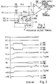
- the first embodiment of this invention will be described by reference to FIG. 5.
- the components identical to those of the chopper type differential amplifier shown in FIG. 1 are assigned identical reference numerals to omit a further description.
- This embodiment has a feature in a precharging circuit 41.
- the precharging circuit 41 comprises a precharging voltage terminal 4 which is supplied with a voltage Vp higher than the power supply voltage Vdd, an N-channel MOS-FET QN11 having a gate electrode supplied with a sampling signal S11 and the source-drain path connected between the input end 2 of the differential amplifier 1 and the precharging voltage terminal 4, and an N-channel MOS-FET QN12 having a gate electrode supplied with the sampling signal S11 and the source-drain path connected between the input end 3 of the differential amplifier 1 and the precharging voltage terminal 4.
- the precharging voltage Vp is an externally supplied boost-up voltage or a boost-up voltage generated by an internal boost-up circuit.
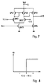
- FIG. 7 A specific circuit configuration of the differential amplifier 1 is shown in FIG. 7.
- Input signals V(+) and V(-) are supplied to N-channel MOS-FETs QN22 and QN21, respectively, and a constant voltage Vc is supplied to the gate electrodes of N-channel MOS-FETs QN23 and QN24.
- the output signal VO is taken out from the junction of a P-channel MOS-FET QP23 and the N-channel MOS-FET QN24. As shown in FIG. 8, the output signal VO is at a low level when the difference of the two input signals (V(+) - V(-)) is negative, and at a high level when it is positive.
- the operation of the chopper type differential amplifier shown in FIG. 5 will be described.
- the embodiment will be described for the case where the input signal V(+) is a signal whose potential varies in the range from 0V to Vdd, while the input signal V(-) has a constant value.
- the input signals VI(+) and VI(-) are applied to the lower electrodes of the MOS gate capacitors CG1 and CG2 and the sampling signal S11 goes to the high level, therefore the N-channel MOS-FETs QN11 and QN12 are turned on.
- the input ends 2 and 3 (the gate electrodes of the MOS gate capacitors CG1 and CG2) of the differential amplifier 1 are precharged to the voltage Vp (Vp ⁇ Vdd) of the precharging voltage terminal 4.
- the high level VH1 of the sampling signal S11 is set to satisfy the relation VH1 ⁇ Vp + V TN , where V TN is the threshold voltage of the N-channel MOS-FETs QN11 and QN12.
- the sampling signal S11 goes to the low level and the N-channel MOS-FETs QN11 and QN12 are turned off. Charge which stored in the MOS gate capacitors CG1 and CG2 are conserved, and an input signal (VI(+) in this embodiment) undergoes a change.
- the input signal VI(+) is raised slightly as shown by the solid line in FIG. 6, the potential of the input end 2 of the differential amplifier 1 also goes to a potential slightly higher than that of the precharging signal Vp, and a high level output signal VO shown by the solid line is output from the output terminal of the differential amplifier 1.
- the MOS gate capacitors CG1 and CG2 always hold the relation V GS ⁇ 0V for the voltage V GS between the gate electrode and the lower electrode.
- the capacitances of the MOS gate capacitors CG1 and CG2 are constant (C OX ) independent of the potentials of the input signals and will not show an unbalance.
- the bias dependence of the MOS gate capacitor is shifted due to the capture of electric charges by the interface between the gate insulating film and the silicon crystal or to the difference in the work functions of the gate electrode and the silicon crystal is a well-known fact.
- the bias dependence of the capacitance is shifted in the positive direction by the amount coresponding to the voltage V SH as shown by the broken line in FIG. 4.
- the precharging voltage Vp is set to a value higher than the power supply voltage Vdd of the differential amplifier 1 by more than the amount corresponding to V SH , namely, to Vp ⁇ Vdd + V SH . Since the MOS gate capacitors CG1 and CG2 are always biased so as to satisfy V GS ⁇ V SH , the capacitances of the MOS gate capacitors CG1 and CG2 become constant independent of the potentials of the input signals.
- the precharging circuit 42 includes a diode-connected N-channel MOS-FET QN13 having its gate electrode and the drain electrode connected to a junction node N and its source electrode connected to the input end 2 of the differential amplifier 1, a diode-connected N-channel MOS-FET QN14 having its gate electrode and the drain electrode connected to the junction node N and its source electrode connected to the input end 3 of the differential amplifier 1, an N-channel MOS-FET QN15 having a gate electrode supplied with a sampling signal S12 and its drain electrode and source electrode connected to the precharging voltage terminal 4 (with voltage Vdd) and the junction node N, respectively, and a capacitance element C11 whose one end is connected to the junction node N and the other end connected to a sampling signal S13.
- the sampling signal S12 is applied to the gates of the N-channel MOS-FETs QN11, QN12 and QN15.
- Vp Vdd in this embodiment, in contrast to Vp ⁇ Vdd in the first embodiment.
- VH Vdd .
- Vdd the high level
- VA Vdd-V TN
- V TN the threshold voltage of the N-channel MOS-FETs QN11, QN12 and QN15.
- VTN is the threshold voltage of the N-channel MOS-FETs QN13 and QN14. Consequently, the N-channel MOS-FETs QN13 and QN14 are turned off again.
- the input signal VI(+) undergoes a change to output an output signal.
- the potentials of the two input ends 2 and 3 of the differential amplifier 1 that is, the gate electrode potentials of the MOS gate capacitors CG1 and CG2, to be equal to or higher than the power supply voltage Vdd of the differential amplifier 1. Accordingly, the capacitances of the MOS gate capacitors CG1 and CG2 are constant regardless of the potentials of the input signals, and hence an output signal of the correct level can be output even if an in-phase noise is applied to the two input ends 2 and 3 of the differential amplifier 1.
- a boost-up means such as a charge pump due to the fact that Vp and the high level of the sampling signal S11 have voltage values higher than the power supply voltage Vdd.
- a boost-up means such as a charge pump due to the fact that Vp and the high level of the sampling signal S11 have voltage values higher than the power supply voltage Vdd.
- an additional voltage boost-up means such as a charge pump is not called for.
- a sampling signal S14 is applied to the gate electrodes, and an equalizing N-channel MOS-FET QN16 with its drain electrode and source electrode connected to the input ends 2 and 3, respectively, of the differential amplifier 1 are provided in addition to the second embodiment shown in FIG. 9.
- the operation of the equalizing N-channel MOS-FET QN16 will be described.
- the sampling period the period in which the sampling signal S13 is at the high level following the sampling signal S12
- the sampling signal S14 is at the high level and the equalizing N-channel MOS-FET QN16 is kept turned on. Accordingly, the two input ends 2 and 3 of the differential amplifier 1 are short-circuited, and an offset voltage generated during the sampling period is canceled.
- the high level voltage V H4 of the sampling signal S14 is set to satisfy V H4 ⁇ V(+) + V TN , where V TN is the threshold voltage of the equalizing N-channel MOS-FET QN16. In this embodiment, malfunctions will not be generated either since the correct output signal is output all the time regardless of an in-phase noise applied to the two input ends of the differential amplifier 1.
- the capacitances of the MOS gate capacitors for input can be kept constant without causing an unbalance regardless of the potentials of the input signals. Consequently, the correct output signal can always be output even if an in-phase noise is applied to the two input ends of the differential amplifier, so that it is possible to provide a chopper type differential amplifier having an excellent noise resistance and being free from malfunctions.
Landscapes
- Engineering & Computer Science (AREA)
- Power Engineering (AREA)
- Physics & Mathematics (AREA)
- Nonlinear Science (AREA)
- Amplifiers (AREA)
- Analogue/Digital Conversion (AREA)
Applications Claiming Priority (3)
| Application Number | Priority Date | Filing Date | Title |
|---|---|---|---|
| JP19378693 | 1993-08-05 | ||
| JP193786/93 | 1993-08-05 | ||
| JP5193786A JP2503902B2 (ja) | 1993-08-05 | 1993-08-05 | チョッパ型差動増幅器 |
Publications (2)
| Publication Number | Publication Date |
|---|---|
| EP0638996A1 true EP0638996A1 (de) | 1995-02-15 |
| EP0638996B1 EP0638996B1 (de) | 1999-09-29 |
Family
ID=16313776
Family Applications (1)
| Application Number | Title | Priority Date | Filing Date |
|---|---|---|---|
| EP94112234A Expired - Lifetime EP0638996B1 (de) | 1993-08-05 | 1994-08-04 | Chopper-Differenzverstärker mit MOS-Kondensatoren |
Country Status (5)
| Country | Link |
|---|---|
| US (1) | US5477186A (de) |
| EP (1) | EP0638996B1 (de) |
| JP (1) | JP2503902B2 (de) |
| KR (1) | KR0146914B1 (de) |
| DE (1) | DE69420919T2 (de) |
Cited By (4)
| Publication number | Priority date | Publication date | Assignee | Title |
|---|---|---|---|---|
| EP1154564A3 (de) * | 2000-05-13 | 2006-03-15 | Micronas GmbH | Zweistufiger Verstärker |
| EP2320296A1 (de) * | 2009-10-30 | 2011-05-11 | STMicroelectronics S.r.l. | Schaltung zur Erzeugung einer Referenzspannung mit Kompensation der Offset-Spannung |
| EP2320295A1 (de) * | 2009-10-30 | 2011-05-11 | STMicroelectronics S.r.l. | Kreis zur Erzeugung einer Referenzspannung |
| CN111682853A (zh) * | 2020-06-15 | 2020-09-18 | 电子科技大学 | 一种电容耦合斩波放大器的交替电容网络 |
Families Citing this family (4)
| Publication number | Priority date | Publication date | Assignee | Title |
|---|---|---|---|---|
| US6195027B1 (en) | 1999-04-30 | 2001-02-27 | International Business Machines Corporation | Capacitive precharging and discharging network for converting N bit input into M bit output |
| KR20030003923A (ko) * | 2001-07-04 | 2003-01-14 | 엘지전자 주식회사 | 의류 건조기의 구동장치 |
| US6906591B2 (en) * | 2002-11-29 | 2005-06-14 | Sigmatel, Inc. | Amplifier having MOS capacitor compensation |
| KR101406470B1 (ko) * | 2013-04-02 | 2014-06-16 | 중앙대학교 산학협력단 | 쵸핑을 이용한 rf 수신기 및 이에 구비된 증폭기 |
Citations (4)
| Publication number | Priority date | Publication date | Assignee | Title |
|---|---|---|---|---|
| US4553052A (en) * | 1982-04-23 | 1985-11-12 | Nec Corporation | High speed comparator circuit with input-offset compensation function |
| US4611130A (en) * | 1984-02-13 | 1986-09-09 | At&T Bell Laboratories | Floating input comparator with precharging of input parasitic capacitors |
| US4883987A (en) * | 1988-05-04 | 1989-11-28 | Texas Instruments Incorporated | Comparator circuit having a fast recovery time |
| GB2258779A (en) * | 1989-02-08 | 1993-02-17 | Burr Brown Corp | Fet differential amplifier with output offset correction. |
Family Cites Families (1)
| Publication number | Priority date | Publication date | Assignee | Title |
|---|---|---|---|---|
| US5142238A (en) * | 1991-07-18 | 1992-08-25 | Silicon Systems, Inc. | Switched-capacitor differential amplifier |
-
1993
- 1993-08-05 JP JP5193786A patent/JP2503902B2/ja not_active Expired - Lifetime
-
1994
- 1994-08-04 DE DE69420919T patent/DE69420919T2/de not_active Expired - Fee Related
- 1994-08-04 EP EP94112234A patent/EP0638996B1/de not_active Expired - Lifetime
- 1994-08-05 KR KR1019940019388A patent/KR0146914B1/ko not_active Expired - Fee Related
- 1994-08-05 US US08/286,456 patent/US5477186A/en not_active Expired - Fee Related
Patent Citations (4)
| Publication number | Priority date | Publication date | Assignee | Title |
|---|---|---|---|---|
| US4553052A (en) * | 1982-04-23 | 1985-11-12 | Nec Corporation | High speed comparator circuit with input-offset compensation function |
| US4611130A (en) * | 1984-02-13 | 1986-09-09 | At&T Bell Laboratories | Floating input comparator with precharging of input parasitic capacitors |
| US4883987A (en) * | 1988-05-04 | 1989-11-28 | Texas Instruments Incorporated | Comparator circuit having a fast recovery time |
| GB2258779A (en) * | 1989-02-08 | 1993-02-17 | Burr Brown Corp | Fet differential amplifier with output offset correction. |
Cited By (6)
| Publication number | Priority date | Publication date | Assignee | Title |
|---|---|---|---|---|
| EP1154564A3 (de) * | 2000-05-13 | 2006-03-15 | Micronas GmbH | Zweistufiger Verstärker |
| EP2320296A1 (de) * | 2009-10-30 | 2011-05-11 | STMicroelectronics S.r.l. | Schaltung zur Erzeugung einer Referenzspannung mit Kompensation der Offset-Spannung |
| EP2320295A1 (de) * | 2009-10-30 | 2011-05-11 | STMicroelectronics S.r.l. | Kreis zur Erzeugung einer Referenzspannung |
| US8482342B2 (en) | 2009-10-30 | 2013-07-09 | Stmicroelectronics S.R.L. | Circuit for generating a reference voltage with compensation of the offset voltage |
| US8704588B2 (en) | 2009-10-30 | 2014-04-22 | Stmicroelectronics S.R.L. | Circuit for generating a reference voltage |
| CN111682853A (zh) * | 2020-06-15 | 2020-09-18 | 电子科技大学 | 一种电容耦合斩波放大器的交替电容网络 |
Also Published As
| Publication number | Publication date |
|---|---|
| KR0146914B1 (ko) | 1998-12-01 |
| US5477186A (en) | 1995-12-19 |
| JP2503902B2 (ja) | 1996-06-05 |
| KR950007271A (ko) | 1995-03-21 |
| DE69420919D1 (de) | 1999-11-04 |
| JPH0750529A (ja) | 1995-02-21 |
| DE69420919T2 (de) | 2000-02-24 |
| EP0638996B1 (de) | 1999-09-29 |
Similar Documents
| Publication | Publication Date | Title |
|---|---|---|
| KR910001643B1 (ko) | 승압회로 | |
| US7358946B2 (en) | Offset cancel circuit of voltage follower equipped with operational amplifier | |
| KR100555352B1 (ko) | 레벨 시프트 회로 | |
| US5614851A (en) | High-accuracy, low-power peak-to-peak voltage detector | |
| US6014042A (en) | Phase detector using switched capacitors | |
| EP0090349B1 (de) | Spannungsvergleichsschaltung | |
| US6275094B1 (en) | CMOS device and circuit and method of operation dynamically controlling threshold voltage | |
| US5568093A (en) | Efficient, high frequency, class A-B amplifier for translating low voltage clock signal levels to CMOS logic levels | |
| US5247210A (en) | Method and circuitry for decreasing the recovery time of an MOS differential voltage comparator | |
| EP0231204A4 (de) | Substratvorspannungsgenerator. | |
| EP0638996A1 (de) | Chopper-Differenzverstärker mit MOS-Kondensatoren | |
| WO1995020268A1 (en) | Semiconductor device | |
| KR100278608B1 (ko) | 문턱전압 보상회로 | |
| US5627739A (en) | Regulated charge pump with low noise on the well of the substrate | |
| EP3593220B1 (de) | Niederspannungs-referenzstromschaltung | |
| US4633101A (en) | Semiconductor sample and hold switching circuit | |
| US7372319B1 (en) | Constant boosted voltage generator circuit for feedback switches in a switched capacitor circuit | |
| US4752704A (en) | Noise suppression interface circuit for non-superimposed two-phase timing signal generator | |
| EP0280097A2 (de) | Ladungstransfervorrichtung mit Verstärker | |
| US4687998A (en) | Pulse width generating circuit synchronized with clock signal and corresponding to a reference voltage | |
| EP0691656B1 (de) | Abtast- und Halteschaltung | |
| US4250408A (en) | Clock pulse amplifier and clipper | |
| US5065056A (en) | Clamping circuit | |
| US5589784A (en) | Method and apparatus for detecting changes in a clock signal to static states | |
| JPH0582741A (ja) | Mosキヤパシタ |
Legal Events
| Date | Code | Title | Description |
|---|---|---|---|
| PUAI | Public reference made under article 153(3) epc to a published international application that has entered the european phase |
Free format text: ORIGINAL CODE: 0009012 |
|
| AK | Designated contracting states |
Kind code of ref document: A1 Designated state(s): DE FR GB |
|
| 17P | Request for examination filed |
Effective date: 19950601 |
|
| 17Q | First examination report despatched |
Effective date: 19980612 |
|
| GRAG | Despatch of communication of intention to grant |
Free format text: ORIGINAL CODE: EPIDOS AGRA |
|
| GRAG | Despatch of communication of intention to grant |
Free format text: ORIGINAL CODE: EPIDOS AGRA |
|
| GRAH | Despatch of communication of intention to grant a patent |
Free format text: ORIGINAL CODE: EPIDOS IGRA |
|
| GRAH | Despatch of communication of intention to grant a patent |
Free format text: ORIGINAL CODE: EPIDOS IGRA |
|
| GRAA | (expected) grant |
Free format text: ORIGINAL CODE: 0009210 |
|
| AK | Designated contracting states |
Kind code of ref document: B1 Designated state(s): DE FR GB |
|
| REF | Corresponds to: |
Ref document number: 69420919 Country of ref document: DE Date of ref document: 19991104 |
|
| ET | Fr: translation filed | ||
| PLBE | No opposition filed within time limit |
Free format text: ORIGINAL CODE: 0009261 |
|
| STAA | Information on the status of an ep patent application or granted ep patent |
Free format text: STATUS: NO OPPOSITION FILED WITHIN TIME LIMIT |
|
| 26N | No opposition filed | ||
| PGFP | Annual fee paid to national office [announced via postgrant information from national office to epo] |
Ref country code: DE Payment date: 20010730 Year of fee payment: 8 |
|
| PGFP | Annual fee paid to national office [announced via postgrant information from national office to epo] |
Ref country code: GB Payment date: 20010801 Year of fee payment: 8 |
|
| PGFP | Annual fee paid to national office [announced via postgrant information from national office to epo] |
Ref country code: FR Payment date: 20010810 Year of fee payment: 8 |
|
| REG | Reference to a national code |
Ref country code: GB Ref legal event code: IF02 |
|
| PG25 | Lapsed in a contracting state [announced via postgrant information from national office to epo] |
Ref country code: GB Free format text: LAPSE BECAUSE OF NON-PAYMENT OF DUE FEES Effective date: 20020804 |
|
| PG25 | Lapsed in a contracting state [announced via postgrant information from national office to epo] |
Ref country code: DE Free format text: LAPSE BECAUSE OF NON-PAYMENT OF DUE FEES Effective date: 20030301 |
|
| GBPC | Gb: european patent ceased through non-payment of renewal fee |
Effective date: 20020804 |
|
| PG25 | Lapsed in a contracting state [announced via postgrant information from national office to epo] |
Ref country code: FR Free format text: LAPSE BECAUSE OF NON-PAYMENT OF DUE FEES Effective date: 20030430 |
|
| REG | Reference to a national code |
Ref country code: FR Ref legal event code: ST |