EP0280097A2 - Ladungstransfervorrichtung mit Verstärker - Google Patents
Ladungstransfervorrichtung mit Verstärker Download PDFInfo
- Publication number
- EP0280097A2 EP0280097A2 EP88101709A EP88101709A EP0280097A2 EP 0280097 A2 EP0280097 A2 EP 0280097A2 EP 88101709 A EP88101709 A EP 88101709A EP 88101709 A EP88101709 A EP 88101709A EP 0280097 A2 EP0280097 A2 EP 0280097A2
- Authority
- EP
- European Patent Office
- Prior art keywords
- mos transistor
- type mos
- current path
- voltage
- reference voltage
- Prior art date
- Legal status (The legal status is an assumption and is not a legal conclusion. Google has not performed a legal analysis and makes no representation as to the accuracy of the status listed.)
- Granted
Links
Images


Classifications
-
- H—ELECTRICITY
- H04—ELECTRIC COMMUNICATION TECHNIQUE
- H04N—PICTORIAL COMMUNICATION, e.g. TELEVISION
- H04N5/00—Details of television systems
- H04N5/30—Transforming light or analogous information into electric information
-
- G—PHYSICS
- G11—INFORMATION STORAGE
- G11C—STATIC STORES
- G11C27/00—Electric analogue stores, e.g. for storing instantaneous values
- G11C27/04—Shift registers
-
- G—PHYSICS
- G11—INFORMATION STORAGE
- G11C—STATIC STORES
- G11C19/00—Digital stores in which the information is moved stepwise, e.g. shift registers
- G11C19/28—Digital stores in which the information is moved stepwise, e.g. shift registers using semiconductor elements
- G11C19/282—Digital stores in which the information is moved stepwise, e.g. shift registers using semiconductor elements with charge storage in a depletion layer, i.e. charge coupled devices [CCD]
- G11C19/285—Peripheral circuits, e.g. for writing into the first stage; for reading-out of the last stage
-
- H—ELECTRICITY
- H10—SEMICONDUCTOR DEVICES; ELECTRIC SOLID-STATE DEVICES NOT OTHERWISE PROVIDED FOR
- H10D—INORGANIC ELECTRIC SEMICONDUCTOR DEVICES
- H10D48/00—Individual devices not covered by groups H10D1/00 - H10D44/00
- H10D48/30—Devices controlled by electric currents or voltages
- H10D48/32—Devices controlled by only the electric current supplied, or only the electric potential applied, to an electrode which does not carry the current to be rectified, amplified or switched
- H10D48/36—Unipolar devices
Definitions
- the present invention relates to an output unit for a charge transfer device (hereinafter referred to as a "CTD”) and, more particularly, to a reference voltage generator for a voltage step-up circuit for applying a stepped-up voltage to a drain.
- CTD charge transfer device
- CTDs are widely used in solid state image sensors, charge transfer type delay lines, comb line filters, transversal filters, and so forth.
- a floating diffusion system is a known type of semiconductor integrated CTD signal output system.
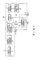
- One of a number of CTDs which employ a floating diffusion system with step-up circuit is disclosed in Figs. 4 and 5 of Japanese Patent Disclosure Sho 59-132668, invented by the inventor of the present invention, Mr. lmai. The construction and the operation of the CTD with the step-up circuit will be described with reference to Figs. 1 and 2.
- An analog signal is input through terminal 1 to input unit 7 of CTD shown in Figs. 1 and 2.
- Input unit 7 converts the input signal to a signal charge whose charge amount is corresponding to the level of the input signal, and also adds to this signal charge a predetermined DC bias charge.
- the resulting signal charge is then transferred toward floating diffusion region 9 by charge transfer unit 8.
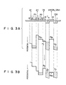
- Charge transfer unit 8 comprises a front surface region of semiconductor substrate 5 and transfer electrodes 17i, 18i (i is 1 to n). Transfer electrodes 17i, 18i transfer the signal charges of semiconductor substrate 5 according to two clock pulses 01, 02.
- the transferred signal charges are fed under output gate electrode 10 to floating diffusion region 9.
- Reset voltage VGG higher than power source voltage VDD, is applied by step-up circuit 19 to drain region 11.
- FET 14 of output circuit 16 is connected at its gate to floating diffusion region 9, and a constant current flows from current source 15 to a current path. FET 14 converts the signal charge fed to floating diffusion region 9 to voltage signal, and outputs voltage signal VOUT.
- the CTD can increase the charge containing capacity of floating diffusion region 9 without increasing the capacity of floating diffusion region 9.
- Step-up circuit 19 for applying voltage VGG higher than power source voltage VDD to drain region 11 will be described.
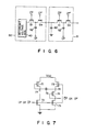
- Fig. 4 shows a step-up circuit disclosed in Fig. 7 of the Japanese Patent Disclosure.
- Step-up circuit 19 in Fig. 4 has reference voltage generator 20 including depletion type MOS transistors 21, 22; and step-up portion 30 including MOS transistor 31, MOS transistor 32 and capacitor 33.
- MOS transistors 21, 22 have the same conductivity type as that of MOS transistor (MOS transistor including regions 9, 11 and electrode 13) for forming reset means 12 of the CTD.
- the lower limit of voltage VGG must be larger than potential value PnL under the transfer electrode 18n. Therefore, the following equation (7) is satisfied.
- Threshold value VTHD of the depletion transistor and threshold value VTHE of the enhancement transistor are independently varied by process variations, e.g., the thickness of insulating film 6 in Fig. 2, the irregularity of ion density of ions to be implanted, the depth of the layer of implanted ions, and the irregular gate of the impurity density of the semiconductor substrate.
- reference voltage generator 20 in Fig. 4 is composed of the same conductivity type MOS transistors, output voltage VGG is constant irrespective of the process variations.
- I VTHD I is, for example, large, the tolerance of the lower limit of VFD is small from equation (7), and when VTHE is small, the tolerance of the upper limit of the VFD is mall from equation (7).
- an object of the present invention is to provide a charge transfer device with a voltage step-up circuit which does not reduce the margin of a range of a signal voltage of in a floating diffusion region due to a process variation and can provide good linearity and S/N at a predetermined power source voltage to produce an output signal of wide dynamic range.
- Another object of the present invention is to provide an output unit for a charge transfer device with a voltage step-up circuit which can produce an output signal of a predetermined level with good linearity and S/N at a low power source voltage.
- a charge transfer device comprising:
- the output voltage (VREF) of the reference voltage generator follows to the process variation. Therefore, the output (VGG) of the voltage step-up circuit 19 also follows the process variation.
- the dynamic range of the output signal of the charge transfer device can be maintained constant irrespective of a certain degree of process variation.
- the merits can be sufficiently provided by using the voltage step-up circuit to obtain a large dynamic range, good linearity and high S/N.
- the feature of the embodiment resides in that voltage VGG is varied in response to the degree of variation in threshold values VTHD , VTHE in the equation (7).
- the output voltage of the reference voltage source of the voltage step-up circuit depends upon the process variation.
- the voltage step-up circuit of embodiments of the present invention will be described with reference to Figs. 1, 2 and 5.
- Fig. 5 shows a voltage step-up circuit according to an embodiment of the present invention.
- the voltage step-up circuit of Fig. 5 comprises reference voltage generator 40 and step-up portion 50.
- Reference voltage generator 40 comprises depletion type (D type) MOS transistor 41 connected at its drain to a VDD power source node, and connected at its source and gate to reference voltage output terminal 43; and enhancement type (E type) MOS transistor 42 connected at its source to VSS power source node and connected at its drain and gate to reference voltage output terminal 43.
- enhancement type (E type) MOS transistor 42 connected at its source to VSS power source node and connected at its drain and gate to reference voltage output terminal 43.
- Step-up portion 50 comprises first E type MOS transistor 51 connected at one end of a current path to reference voltage output terminal 43 for applying clock pulse CP to its gate; capacitor 52 connected at its one end to the other end of the current path of first E type MOS transistor 51 for applying clock pulse CP to its other end; and second E type MOS transistor 54 connected at its one end of the current path to the connecting node 53 of first E type MOS transistor 51 and capacitor 52 for applying clock pulse CP' to its gate to generate output voltage VGG of a voltage step-up circuit 19 to other end 55 of the current path.
- Clock pulse CP' has the same phase as clock pulse CP, and has a high level which is higher by voltage level corresponding to threshold value VTHE of MOS transistor 54 than the high level of the clock pulse generated at node 53.
- D type MOS transistor 41 has the same conductivity type and the same construction as a MOS transistor (having regions 9, 11, and electrode 13 of Fig. 2) for forming CTD reset circuit (12 in Fig. 1).
- D type MOS transistor 41 is manufactured in the same process as a MOS transistor for forming reset circuit 12, and is saturated.
- E type MOS transistor 42 has the same conductivity type (N type in Fig. 2) as MOS transistor (14 in Fig. 2) connected at its gate to the floating diffusion region (9 in Fig. 2) of CTD, and is saturated.
- VTHE 1V
- VTHD -6V
- 0.2
- ⁇ 42/ ⁇ 41 2.0
- VREF 3.64V is obtained.
- VTHE 1 ⁇ 0.4V
- VTHD -6 ⁇ 1 V due to the process variation.
- reference voltage VREF varies in response to the variation in the threshold voltages of transistors 41, 42 due to process variation.
- the variation in reference voltage output (process dependency) reflects output voltage VGG of voltage step-up circuit 19.
- VGG becomes high. Therefore, as understood from the equation (7), bias voltage VFD of signal in floating diffusion region 9 becomes high, and both upper and lower limits of the equation (7) are shifted to higher positions.
- the tolerance of the operating range of the signal charge is increased as compared with the case that reference voltage VREF is fixed.
- VGG becomes low. Therefore, as understood from the equation (7), bias voltage VFD of signal in floating diffusion region 9 becomes low, and both upper and lower limits of the equation (7) are shifted to lower positions.
- the voltage step-up circuit of the invention is not limited to the construction in Fig. 5.
- step-up portion 30 in Fig. 4 may be used instead of step-up portion 50 in Fig. 5.
- the output voltage of voltage step-up circuit 19 is reduced by the threshold voltage of MOS diode 32 as compared with output voltage VGG of the voltage step-up circuit of Fig. 5 by the operation of MOS diode 32. Therefore, it is necessary to set the reference voltage higher by threshold value VTHE (1V in the above example) of MOS diode 32 in Fig. 4 than the reference voltage of Fig. 5 under process center conditions. Thus, values of MOS transistors 41, 42 are altered.
- MOS transistors 31, 51 may be replaced by depletion type MOS transistors or MOS diodes.
- Transistors 32, 54 may be replaced by depletion type MOS transistors. When the depletion type MOS transistors are used, it is necessary to apply a clock pulse of the voltage relation that the transistors are completely turned OFF when a low level clock is applied to the gates and transistors are completely turned ON when a high level clock is applied.
- a voltage step-up circuit in Fig. 6 may also be employed.
- the voltage step-up circuit in Fig. 6 the voltage step-up circuit in Fig. 5 is connected in a cascade, the input terminal of second stage voltage step-up circuit 61 is connected to the output terminal of the first stage voltage step-up circuit 60, and the reference voltage generator is replaced with a capacitor 62.
- normal clock pulses CP, CP and CP' (which has stepped-up high level) are supplied to the first stage voltage step-up circuit 60.
- clock pulse CP' and CP" which have been stepped-up to a high level are applied.
- Clock pulses CP' and CP' are, for example, obtained by voltage step-up circuit 70 having transistors 71 to 75, and capacitor 76 in Fig. 7.
- clock pulse CP or CP when clock pulse CP or CP is high level, node 77 is low level, and transistors 73, 75 are turned ON. Capacitor 76 is charged, and voltage of one terminal 78 of capacitor 76 becomes VDD. At this time, CP' or CP' becomes low level (substantially ground level).
- clock pulse CP or CP is low level, node 77 is high level, and transistors 73, 75 are turned OFF. The voltage of one terminal 78 of capacitor 76 becomes 2VDD(VDD + VDD), and this voltage become CP' or CP'.
- Clock pulse CP" varies from 0V to 3VDD at level synchronously with clock pulse CP and obtained by a circuit similar to Fig. 7.
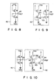
- Reference voltage generator 80 in Fig. 8 comprises a D type MOS transistor 81 connected at its drain and gate to the VDD power source node, and connected at a source to reference voltage output terminal 83 for operating in a nonsaturated state; and an E type MOS transistor 82 connected at its source to the VSS voltage source, and connected at its gate and source to reference voltage output terminal 83.
- reference voltage VREF follows the process variation in the same manner as the case that reference voltage generator 40 of Fig. 5 is used.
- the drain and the gate of E type MOS transistor 91 are connected to VDD power source node, and the gate and the source of D type MOS transistor 92 are connected to VSS voltage source.
- the gate of E-type transistor 42 in reference voltage generator circuit 40 in Fig. 5 is switching connected from a reference voltage output terminal to junction 93 between transistors 91 and 92.
- Transistors 41 and 42 have their junction taken out as reference output voltage terminal 94.
- E type MOS transistor 91 and D type MOS transistor 92 have greater VTHE and VTHD : levels, respectively, the gate voltage VG1 becomes small so that the mutual conductance gm of E type MOS transistor 42 is lowered by a greater extent of VTHE plus a smaller extent of VG1.
- E type MOS transistor 91 and D type MOS transistor 92 have smaller VTHE and
- reference voltage generator circuit 90 has a much better process tracing characteristic than that of reference voltage generator circuit 40. It is to be noted that the same effect is also obtained even if the gate of D type MOS transistor 41 in Fig. 9 is connected to VDD power source node instead.
- Fig. 10 shows a reference voltage generator of such a type as used as reference voltage generator 40 in Fig. 5 and as reference voltage generator of Fig. 9.
- the gate of D type MOS transistor 41 in circuit 90 is switching connected from output terminal 94 to reference voltage output terminal 43.
- VTHD I of D type MOS transistor 41 and VTHE of E type MOS transistor 42 are large, gate voltage VG2 becomes large. Therefore, trans-conductance gm of D type MOS transistor 41 of reference voltage generator 90 is increased in the amount that I VTHD is large and VG2 is large.
- i VTHD of D type MOS transistor 41 of circuit 40 is small and VTHE of E type MOS transistor 42 is small, gate voltage VG2 is reduced.
- reference voltage generator 80 of Fig. 8 or reference voltage generator 90 of Fig. 9 may be used instead of circuit 40.
- a plurality of circuits 90 are provided and may be connected in cascade so that the output voltages of the front stage circuits are connected to the input of the rear stage circuits.
- D type MOS transistor for forming the reference voltage generator of the same process as the transistor for forming a reset circuit 12 to perform the process followability of the reference voltage generator.
- D type MOS transistors are manufactured in the same process and E type MOS transistors are manufactured in the same process, because the process variation affects the transistors in an equal ratio.
- floating diffusion region 9, drain region 11, and source region 411 and drain region 412 of transistor 41 are formed by thermal diffusion in semiconductor substrate 5.
- Impurity ions X are implanted under the same conditions to a region between regions 9 and 11 and channel region between source region 411 and drain region 412.
- insulating film 6 is formed on semiconductor substrate 5.
- Polysilicon layer (so-called first polysilicon layer) is formed on insulating film 6.
- First polysilicon layer is patterned, and as shown in Fig. 11 C, reset electrode 13 and gate electrode 413 of transistor 41 are formed together with transfer electrode 18i.
- insulating layer 110 is formed. An opening for forming electrode 17i is formed on insulating layer 110.
- Polysilicon layer (so-called second polysilicon layer) is formed on insulating layer 110, and patterned to form transfer electrode 17i, and output gate electrode 10 as shown in Fig. 11 E.
- D type MOS transistor 41 and MOS transistor for forming reset circuit 12 are formed in the same steps and have the same constitution. Therefore, the variations in the thicknesses of the insulating films, electrode forming conditions, variations in the impurity densities in substrates, channel regions, semiconductor layers equally affect both the transistors to complete the process followability. In other words, when the transistors are formed as described above, the ratio of displacement from the process center of the process in a certain pellet equally affect the elements on the wafer, thereby accomplishing the desired effects.
- the above manufacturing steps are by way of example only, and the manufacturing steps are not limited to the embodiment.
- the voltage step-up circuit is provided. Therefore, the output signal of large level having good linearity and high SiN can be obtained under predetermined power source voltage. Or, the power source voltage necessary to obtain the output signal of a predetermined level having good linearity and high S/N can be reduced.
- the reference voltage generator of the voltage step-up circuit is ,deviced to provide process followability at the reference voltage output. Therefore, the output voltage of the voltage step-up circuit has the process followability. As a result, even if certain process variation occurs, the dynamic range of the output signal of CTD is widely maintained to obtain the output signal having good linearity and high SiN.
- the circuit formed of N-channel MOS transistors has been described as an example.
- the present invention is not limited to the particular embodiments, but can be similarly applied to the case that P-channel MOS transistors or complementary MOS transistors are employed in the circuit.
Landscapes
- Engineering & Computer Science (AREA)
- Multimedia (AREA)
- Signal Processing (AREA)
- Solid State Image Pick-Up Elements (AREA)
Applications Claiming Priority (2)
| Application Number | Priority Date | Filing Date | Title |
|---|---|---|---|
| JP30747/87 | 1987-02-13 | ||
| JP3074787 | 1987-02-13 |
Publications (3)
| Publication Number | Publication Date |
|---|---|
| EP0280097A2 true EP0280097A2 (de) | 1988-08-31 |
| EP0280097A3 EP0280097A3 (en) | 1990-02-28 |
| EP0280097B1 EP0280097B1 (de) | 1992-01-22 |
Family
ID=12312272
Family Applications (1)
| Application Number | Title | Priority Date | Filing Date |
|---|---|---|---|
| EP88101709A Expired - Lifetime EP0280097B1 (de) | 1987-02-13 | 1988-02-05 | Ladungstransfervorrichtung mit Verstärker |
Country Status (4)
| Country | Link |
|---|---|
| US (1) | US4984256A (de) |
| EP (1) | EP0280097B1 (de) |
| KR (1) | KR920001405B1 (de) |
| DE (1) | DE3867863D1 (de) |
Families Citing this family (10)
| Publication number | Priority date | Publication date | Assignee | Title |
|---|---|---|---|---|
| JPH03147488A (ja) * | 1989-11-01 | 1991-06-24 | Olympus Optical Co Ltd | 画像フリーズ用信号処理装置 |
| US5132936A (en) * | 1989-12-14 | 1992-07-21 | Cypress Semiconductor Corporation | MOS memory circuit with fast access time |
| JP3271086B2 (ja) * | 1992-09-29 | 2002-04-02 | ソニー株式会社 | 固体撮像素子の駆動回路 |
| US5412257A (en) * | 1992-10-20 | 1995-05-02 | United Memories, Inc. | High efficiency N-channel charge pump having a primary pump and a non-cascaded secondary pump |
| JP3310164B2 (ja) * | 1996-05-30 | 2002-07-29 | 株式会社東芝 | 固体撮像装置 |
| JP2002140124A (ja) * | 2000-10-30 | 2002-05-17 | Seiko Epson Corp | 基準電圧回路 |
| US8072834B2 (en) | 2005-08-25 | 2011-12-06 | Cypress Semiconductor Corporation | Line driver circuit and method with standby mode of operation |
| KR101554369B1 (ko) * | 2007-01-19 | 2015-09-18 | 인터실 아메리카스 엘엘씨 | 전하영역 파이프라인의 아날로그 디지털 변환기 |
| US7535400B2 (en) * | 2007-01-23 | 2009-05-19 | Kenet, Incorporated | Analog error correction for a pipelined charge-domain A/D converter |
| TWI493851B (zh) * | 2007-12-07 | 2015-07-21 | Intersil Americas LLC | 不變動電荷傳送特性而增加電荷傳送電路的電荷容量之操作方法及電荷傳送級裝置 |
Family Cites Families (17)
| Publication number | Priority date | Publication date | Assignee | Title |
|---|---|---|---|---|
| US3955101A (en) * | 1974-07-29 | 1976-05-04 | Fairchild Camera And Instrument Coporation | Dynamic reference voltage generator |
| US4100437A (en) * | 1976-07-29 | 1978-07-11 | Intel Corporation | MOS reference voltage circuit |
| US4180807A (en) * | 1977-11-17 | 1979-12-25 | General Electric Company | Charge transfer circuit with voltage threshold compensating means |
| US4559638A (en) * | 1978-10-23 | 1985-12-17 | Westinghouse Electric Corp. | Charge transfer device having an improved read-out portion |
| JPS56122526A (en) * | 1980-03-03 | 1981-09-26 | Fujitsu Ltd | Semiconductor integrated circuit |
| JPS6041364B2 (ja) * | 1980-08-29 | 1985-09-17 | 富士通株式会社 | 出力バッファ回路 |
| JPS5875922A (ja) * | 1981-10-30 | 1983-05-07 | Toshiba Corp | 半導体スイツチ回路 |
| US4513431A (en) * | 1982-06-07 | 1985-04-23 | International Business Machines Corporation | Charge coupled device output circuit structure |
| JPS59132668A (ja) * | 1983-01-19 | 1984-07-30 | Toshiba Corp | 電荷転送素子の出力装置 |
| US4614882A (en) * | 1983-11-22 | 1986-09-30 | Digital Equipment Corporation | Bus transceiver including compensation circuit for variations in electrical characteristics of components |
| JPH0756613B2 (ja) * | 1984-09-10 | 1995-06-14 | シャープ株式会社 | 基準電圧発生回路 |
| JPS61187368A (ja) * | 1985-02-15 | 1986-08-21 | Toshiba Corp | 電荷転送装置 |
| NL8500863A (nl) * | 1985-03-25 | 1986-10-16 | Philips Nv | Ladingsoverdrachtinrichting. |
| EP0218747B1 (de) * | 1985-10-15 | 1991-05-08 | International Business Machines Corporation | Leseverstärker zur Verstärkung von Signalen auf einer vorgespannten Leitung |
| US4719372A (en) * | 1986-02-03 | 1988-01-12 | International Business Machines Corporation | Multiplying interface circuit for level shifting between FET and TTL levels |
| JPS62230052A (ja) * | 1986-03-31 | 1987-10-08 | Toshiba Corp | 電荷転送装置 |
| US4686451A (en) * | 1986-10-15 | 1987-08-11 | Triquint Semiconductor, Inc. | GaAs voltage reference generator |
-
1988
- 1988-02-04 US US07/152,382 patent/US4984256A/en not_active Expired - Fee Related
- 1988-02-05 DE DE8888101709T patent/DE3867863D1/de not_active Expired - Lifetime
- 1988-02-05 EP EP88101709A patent/EP0280097B1/de not_active Expired - Lifetime
- 1988-02-13 KR KR1019880001412A patent/KR920001405B1/ko not_active Expired
Also Published As
| Publication number | Publication date |
|---|---|
| KR920001405B1 (ko) | 1992-02-13 |
| US4984256A (en) | 1991-01-08 |
| KR880010607A (ko) | 1988-10-10 |
| DE3867863D1 (de) | 1992-03-05 |
| EP0280097A3 (en) | 1990-02-28 |
| EP0280097B1 (de) | 1992-01-22 |
Similar Documents
| Publication | Publication Date | Title |
|---|---|---|
| US5394359A (en) | MOS integrated circuit with adjustable threshold voltage | |
| US5191398A (en) | Charge transfer device producing a noise-free output | |
| JPH084136B2 (ja) | 電荷転送装置 | |
| EP0280097B1 (de) | Ladungstransfervorrichtung mit Verstärker | |
| EP0292895B1 (de) | Ladungsübertragungsanordnung | |
| JP3401808B2 (ja) | 電荷転送装置 | |
| JPS6233751B2 (de) | ||
| US4974240A (en) | Charge-coupled device floating diffusion output reset | |
| KR910007841B1 (ko) | 전하전송소자 | |
| JPS6038799A (ja) | 半導体不揮発性メモリ用読み出し回路 | |
| US7088393B1 (en) | Output-compensated buffers with source-follower input structure, methods of operating same, and image capture devices using same | |
| JPS6249991B2 (de) | ||
| JPH0787400A (ja) | Ccd固体撮像素子 | |
| US4272693A (en) | Analysis circuit for a charge coupled device | |
| JPS61224357A (ja) | 電荷転送装置 | |
| JPS6251508B2 (de) | ||
| US4266237A (en) | Semiconductor apparatus | |
| US4503550A (en) | Dynamic CCD input source pulse generating circuit | |
| JP2829034B2 (ja) | 半導体回路 | |
| US5172399A (en) | Semiconductor charge transfer device including charge quantity detection | |
| US4890307A (en) | Input circuit of charge transfer device | |
| JPH05119859A (ja) | 基準電圧発生回路 | |
| EP0447917B1 (de) | Ladungsübertragungsvorrichtung | |
| US6191440B1 (en) | Charge transfer device with improved charge detection sensitivity | |
| JPH0263299B2 (de) |
Legal Events
| Date | Code | Title | Description |
|---|---|---|---|
| PUAI | Public reference made under article 153(3) epc to a published international application that has entered the european phase |
Free format text: ORIGINAL CODE: 0009012 |
|
| 17P | Request for examination filed |
Effective date: 19880302 |
|
| AK | Designated contracting states |
Kind code of ref document: A2 Designated state(s): DE FR GB |
|
| PUAL | Search report despatched |
Free format text: ORIGINAL CODE: 0009013 |
|
| AK | Designated contracting states |
Kind code of ref document: A3 Designated state(s): DE FR GB |
|
| 17Q | First examination report despatched |
Effective date: 19910610 |
|
| GRAA | (expected) grant |
Free format text: ORIGINAL CODE: 0009210 |
|
| AK | Designated contracting states |
Kind code of ref document: B1 Designated state(s): DE FR GB |
|
| REF | Corresponds to: |
Ref document number: 3867863 Country of ref document: DE Date of ref document: 19920305 |
|
| ET | Fr: translation filed | ||
| PLBE | No opposition filed within time limit |
Free format text: ORIGINAL CODE: 0009261 |
|
| STAA | Information on the status of an ep patent application or granted ep patent |
Free format text: STATUS: NO OPPOSITION FILED WITHIN TIME LIMIT |
|
| 26N | No opposition filed | ||
| PGFP | Annual fee paid to national office [announced via postgrant information from national office to epo] |
Ref country code: FR Payment date: 19970211 Year of fee payment: 10 |
|
| PGFP | Annual fee paid to national office [announced via postgrant information from national office to epo] |
Ref country code: DE Payment date: 19970214 Year of fee payment: 10 |
|
| PGFP | Annual fee paid to national office [announced via postgrant information from national office to epo] |
Ref country code: GB Payment date: 19980127 Year of fee payment: 11 |
|
| PG25 | Lapsed in a contracting state [announced via postgrant information from national office to epo] |
Ref country code: FR Free format text: THE PATENT HAS BEEN ANNULLED BY A DECISION OF A NATIONAL AUTHORITY Effective date: 19980228 |
|
| PG25 | Lapsed in a contracting state [announced via postgrant information from national office to epo] |
Ref country code: DE Free format text: LAPSE BECAUSE OF NON-PAYMENT OF DUE FEES Effective date: 19981103 |
|
| REG | Reference to a national code |
Ref country code: FR Ref legal event code: ST |
|
| PG25 | Lapsed in a contracting state [announced via postgrant information from national office to epo] |
Ref country code: GB Free format text: LAPSE BECAUSE OF NON-PAYMENT OF DUE FEES Effective date: 19990205 |
|
| GBPC | Gb: european patent ceased through non-payment of renewal fee |
Effective date: 19990205 |