EP0639401B1 - Verfahren zur Behandlung von Molekülen und Vorrichtung dafür - Google Patents
Verfahren zur Behandlung von Molekülen und Vorrichtung dafür Download PDFInfo
- Publication number
- EP0639401B1 EP0639401B1 EP94306029A EP94306029A EP0639401B1 EP 0639401 B1 EP0639401 B1 EP 0639401B1 EP 94306029 A EP94306029 A EP 94306029A EP 94306029 A EP94306029 A EP 94306029A EP 0639401 B1 EP0639401 B1 EP 0639401B1
- Authority
- EP
- European Patent Office
- Prior art keywords
- cold cathode
- metal
- layer
- mim
- initiation
- Prior art date
- Legal status (The legal status is an assumption and is not a legal conclusion. Google has not performed a legal analysis and makes no representation as to the accuracy of the status listed.)
- Expired - Lifetime
Links
- 230000031018 biological processes and functions Effects 0.000 title claims abstract description 13
- 238000000034 method Methods 0.000 claims abstract description 24
- 230000000977 initiatory effect Effects 0.000 claims abstract description 10
- 238000006243 chemical reaction Methods 0.000 claims abstract description 8
- 239000000126 substance Substances 0.000 claims abstract description 8
- 230000000694 effects Effects 0.000 claims abstract description 6
- HEDRZPFGACZZDS-UHFFFAOYSA-N Chloroform Chemical compound ClC(Cl)Cl HEDRZPFGACZZDS-UHFFFAOYSA-N 0.000 claims description 23
- 229910052751 metal Inorganic materials 0.000 claims description 23
- 239000002184 metal Substances 0.000 claims description 23
- 239000012212 insulator Substances 0.000 claims description 4
- RYGMFSIKBFXOCR-UHFFFAOYSA-N Copper Chemical compound [Cu] RYGMFSIKBFXOCR-UHFFFAOYSA-N 0.000 claims description 3
- VYPSYNLAJGMNEJ-UHFFFAOYSA-N Silicium dioxide Chemical group O=[Si]=O VYPSYNLAJGMNEJ-UHFFFAOYSA-N 0.000 claims description 3
- 229910052802 copper Inorganic materials 0.000 claims description 3
- 239000010949 copper Substances 0.000 claims description 3
- 229910052814 silicon oxide Inorganic materials 0.000 claims description 3
- 150000002500 ions Chemical class 0.000 description 7
- 238000010494 dissociation reaction Methods 0.000 description 3
- 230000005593 dissociations Effects 0.000 description 3
- XEEYBQQBJWHFJM-UHFFFAOYSA-N Iron Chemical compound [Fe] XEEYBQQBJWHFJM-UHFFFAOYSA-N 0.000 description 2
- PXHVJJICTQNCMI-UHFFFAOYSA-N Nickel Chemical compound [Ni] PXHVJJICTQNCMI-UHFFFAOYSA-N 0.000 description 2
- 238000006555 catalytic reaction Methods 0.000 description 2
- 238000005323 electroforming Methods 0.000 description 2
- 150000002739 metals Chemical class 0.000 description 2
- 210000003632 microfilament Anatomy 0.000 description 2
- BASFCYQUMIYNBI-UHFFFAOYSA-N platinum Chemical compound [Pt] BASFCYQUMIYNBI-UHFFFAOYSA-N 0.000 description 2
- 239000000376 reactant Substances 0.000 description 2
- 229910052710 silicon Inorganic materials 0.000 description 2
- 239000010703 silicon Substances 0.000 description 2
- VZGDMQKNWNREIO-UHFFFAOYSA-N tetrachloromethane Chemical compound ClC(Cl)(Cl)Cl VZGDMQKNWNREIO-UHFFFAOYSA-N 0.000 description 2
- OKTJSMMVPCPJKN-UHFFFAOYSA-N Carbon Chemical compound [C] OKTJSMMVPCPJKN-UHFFFAOYSA-N 0.000 description 1
- VYZAMTAEIAYCRO-UHFFFAOYSA-N Chromium Chemical compound [Cr] VYZAMTAEIAYCRO-UHFFFAOYSA-N 0.000 description 1
- FYYHWMGAXLPEAU-UHFFFAOYSA-N Magnesium Chemical compound [Mg] FYYHWMGAXLPEAU-UHFFFAOYSA-N 0.000 description 1
- PWHULOQIROXLJO-UHFFFAOYSA-N Manganese Chemical compound [Mn] PWHULOQIROXLJO-UHFFFAOYSA-N 0.000 description 1
- BQCADISMDOOEFD-UHFFFAOYSA-N Silver Chemical compound [Ag] BQCADISMDOOEFD-UHFFFAOYSA-N 0.000 description 1
- ATJFFYVFTNAWJD-UHFFFAOYSA-N Tin Chemical compound [Sn] ATJFFYVFTNAWJD-UHFFFAOYSA-N 0.000 description 1
- HCHKCACWOHOZIP-UHFFFAOYSA-N Zinc Chemical compound [Zn] HCHKCACWOHOZIP-UHFFFAOYSA-N 0.000 description 1
- 239000002156 adsorbate Substances 0.000 description 1
- 239000004411 aluminium Substances 0.000 description 1
- 229910052782 aluminium Inorganic materials 0.000 description 1
- XAGFODPZIPBFFR-UHFFFAOYSA-N aluminium Chemical compound [Al] XAGFODPZIPBFFR-UHFFFAOYSA-N 0.000 description 1
- 229910052790 beryllium Inorganic materials 0.000 description 1
- ATBAMAFKBVZNFJ-UHFFFAOYSA-N beryllium atom Chemical compound [Be] ATBAMAFKBVZNFJ-UHFFFAOYSA-N 0.000 description 1
- 229910052797 bismuth Inorganic materials 0.000 description 1
- JCXGWMGPZLAOME-UHFFFAOYSA-N bismuth atom Chemical compound [Bi] JCXGWMGPZLAOME-UHFFFAOYSA-N 0.000 description 1
- 229910052799 carbon Inorganic materials 0.000 description 1
- 230000015556 catabolic process Effects 0.000 description 1
- 239000003054 catalyst Substances 0.000 description 1
- 229910052804 chromium Inorganic materials 0.000 description 1
- 239000011651 chromium Substances 0.000 description 1
- 230000003749 cleanliness Effects 0.000 description 1
- 229910017052 cobalt Inorganic materials 0.000 description 1
- 239000010941 cobalt Substances 0.000 description 1
- GUTLYIVDDKVIGB-UHFFFAOYSA-N cobalt atom Chemical compound [Co] GUTLYIVDDKVIGB-UHFFFAOYSA-N 0.000 description 1
- 238000009833 condensation Methods 0.000 description 1
- 230000005494 condensation Effects 0.000 description 1
- 239000004020 conductor Substances 0.000 description 1
- 238000003795 desorption Methods 0.000 description 1
- 230000008020 evaporation Effects 0.000 description 1
- 238000001704 evaporation Methods 0.000 description 1
- 230000004907 flux Effects 0.000 description 1
- PCHJSUWPFVWCPO-UHFFFAOYSA-N gold Chemical compound [Au] PCHJSUWPFVWCPO-UHFFFAOYSA-N 0.000 description 1
- 229910052737 gold Inorganic materials 0.000 description 1
- 239000010931 gold Substances 0.000 description 1
- 238000011065 in-situ storage Methods 0.000 description 1
- 239000011810 insulating material Substances 0.000 description 1
- 229910052741 iridium Inorganic materials 0.000 description 1
- GKOZUEZYRPOHIO-UHFFFAOYSA-N iridium atom Chemical compound [Ir] GKOZUEZYRPOHIO-UHFFFAOYSA-N 0.000 description 1
- 229910052742 iron Inorganic materials 0.000 description 1
- 239000011133 lead Substances 0.000 description 1
- 229910052749 magnesium Inorganic materials 0.000 description 1
- 239000011777 magnesium Substances 0.000 description 1
- 229910052748 manganese Inorganic materials 0.000 description 1
- 239000011572 manganese Substances 0.000 description 1
- 238000004519 manufacturing process Methods 0.000 description 1
- 238000004377 microelectronic Methods 0.000 description 1
- 229910052759 nickel Inorganic materials 0.000 description 1
- 229910052697 platinum Inorganic materials 0.000 description 1
- 229910052709 silver Inorganic materials 0.000 description 1
- 239000004332 silver Substances 0.000 description 1
- 238000001228 spectrum Methods 0.000 description 1
- 239000010409 thin film Substances 0.000 description 1
- 239000011135 tin Substances 0.000 description 1
- 229910052718 tin Inorganic materials 0.000 description 1
- WFKWXMTUELFFGS-UHFFFAOYSA-N tungsten Chemical compound [W] WFKWXMTUELFFGS-UHFFFAOYSA-N 0.000 description 1
- 229910052721 tungsten Inorganic materials 0.000 description 1
- 239000010937 tungsten Substances 0.000 description 1
- 229910052725 zinc Inorganic materials 0.000 description 1
- 239000011701 zinc Substances 0.000 description 1
Images


Classifications
-
- C—CHEMISTRY; METALLURGY
- C07—ORGANIC CHEMISTRY
- C07C—ACYCLIC OR CARBOCYCLIC COMPOUNDS
- C07C17/00—Preparation of halogenated hydrocarbons
- C07C17/23—Preparation of halogenated hydrocarbons by dehalogenation
-
- B—PERFORMING OPERATIONS; TRANSPORTING
- B01—PHYSICAL OR CHEMICAL PROCESSES OR APPARATUS IN GENERAL
- B01J—CHEMICAL OR PHYSICAL PROCESSES, e.g. CATALYSIS OR COLLOID CHEMISTRY; THEIR RELEVANT APPARATUS
- B01J19/00—Chemical, physical or physico-chemical processes in general; Their relevant apparatus
- B01J19/08—Processes employing the direct application of electric or wave energy, or particle radiation; Apparatus therefor
- B01J19/087—Processes employing the direct application of electric or wave energy, or particle radiation; Apparatus therefor employing electric or magnetic energy
- B01J19/088—Processes employing the direct application of electric or wave energy, or particle radiation; Apparatus therefor employing electric or magnetic energy giving rise to electric discharges
Definitions
- This invention relates to a method and apparatus for effecting the initiation of molecular processes in substances present on the surface of the apparatus.
- the present invention is concerned with the provision of a novel means of effecting the initiation and/or catalysis of molecular processes by means of the bombardment of molecules by electrons emitted from a particular type of source, which means it allows for good control of the energy of the electrons during the bombardment.
- a method for effecting the initiation of a molecular process or reaction in a substance which comprises bringing the substance into contact with a surface of a cold cathode device and applying an electric potential across the cold cathode device to cause electrons to be emitted from the surface thereof with an energy level sufficient to effect the initiation.
- cold cathode is well known in the electronics art and can be simply defined as a device incorporating an electrode from which electron emission is caused by a high potential gradient across the cold cathode device at normal temperatures, for example, those less than 100°C and commonly ambient temperatures.
- cold cathodes are:
- Cold cathodes generally, and in particular each of the above types of cold cathode device can be operated through the application of, and control of, a voltage across the devices. Control of the voltage is critical to ensure that electrons emitted from the device have the correct level of kinetic energy in particular to effect initiation of the desired molecular process in the substance in contact with the device.
- MIM devices comprise a metal-insulator-metal sandwich in which each metal layer may be of the same or different metal. With a sufficient electric potential (voltage) applied across the device, ie one metal layer being biassed positively and the other negatively with respect to each other, electrons are emitted from the positively biassed metal layer.
- the negatively biassed layer is made of a relatively good conductor, its composition is not particularly critical.
- the selection of the positively biassed layer for which gold, silver, copper, tin, bismuth, cobalt, iron, iridium, nickel, lead and platinum can be employed; most preferably the metal employed for this layer is one of the first four of the above list.
- Other metals which might be employed include aluminium, beryllium, chromium, magnesium, manganese and zinc. Carbon and silicon are also candidates for the positively biassed layer and these elements would be included in the term "metal" for the purposes of this specification.
- the MIM devices operate in practice with an electric potential between the metal layers leading to electron transport from the negatively biassed layer to the positively biassed layer - the device "current" (and thereafter emission from the device) through metallic microfilaments which grow in situ through the insulating layer.
- the process by which these microfilaments are made is sometimes referred to as “electro-forming” or simply “forming” and occurs in the MIM device once a threshold voltage across the device is exceeded.
- the current emitted by the MIM when sufficiently high voltages are applied across the device appears to include a contribution from direct field emission of electrons involving quantum mechanical tunnelling through the device from the negatively biassed metal layer.
- insulator layer thickness is therefore crucial to successful operation of the device; in particular, it must be sufficiently thin that the device current is large enough yet thick enough to prevent dielectric breakdown when the voltages required across the device for electron emission are applied.
- an insulator layer thickness of from 100 to 1,000 angstroms ( ⁇ ) has been found to be useful.
- the thickness is at least 200 ⁇ , for example 300 ⁇ .
- the thickness of the metal layers is not so critical. In general, however, the negatively biassed layer can be as thick as required to conduct the necessary current whereas the positively biassed layer should ideally be as thin as possible to provide maximum electron emission from the device.
- a very thin metal layer may nevertheless be associated with a relatively high electrical resistance and it is expedient to ensure that the resistance of the positively biassed layer, and preferably the other layer also, is sufficiently low, for example less than 40 ohms. This commonly is associated with a metal layer thickness of about 500 to 2,000 ⁇ , for example about 1,000 ⁇ .
- molecules to be the subject of the molecular process can be adsorbed on to a sufficiently cold cathode surface, for example at or (normally) below ambient temperatures that it produces a condensed layer of molecules, the thickness of which is controlled by the amount of gas (ie based on the pressure and dosing time) allowed in to the chamber.
- the molecular process can then proceed when the cathode voltage is turned on.
- the method may involve a flow (or pulses) of gas molecules to be the subject of the molecular process across the surface of the cold cathode device while it is subject to, for example, ambient temperature.
- the pressures at which the chamber in which the molecular processes can be conducted may vary depending on a number of factors. For example, in the first mode of operation above with condensation of molecules on the surface of the device, the process is largely unaffected by pressure overall. The pressure can generally be relatively low with gas being pumped from the chamber during the process. It is possible, however, for the processes to be operated at pressure approaching ambient pressure.
- the process of the invention is in general highly tunable and the energy of electrons emitted by the cold cathode may be chosen to populate the resonance level (negative ion state) of one type of molecule present, ie adsorbed, on the surface rather than another type; another choice of electron energy can select another species.
- the key to the principle of operation of the method of the invention is that electrons are emitted from that surface of the cold cathode onto which the reactant molecules are in contact and adsorbed. The method can therefore operate in a relatively high pressure stream of reactant gas flow.
- Figure 1 shows a microelectronic device for use to initiate and control a chemical reaction. It comprises a thin film metal-insulator-metal (MIM) sandwich in which the metal layers are both copper and the insulating layer is SiO x . All the layers were produced by evaporation from resistively heated boats in ultra-high vacuum.
- MIM metal-insulator-metal
- the cold cathode device shown in Figure 1 was employed to initiate a molecular reaction with chloroform (CCl 3 H) in a reactor chamber.
- the chloroform was introduced into the chamber so that chloroform molecules were adsorbed onto the outer (top) surface of the device and the electron energy of the device was set (by controlling the voltage applied across the device with the positively biassed metal layer at the top) to correspond to a dissociative electron attachment (DA) resonance in the adsorbate, thereby effecting molecular dissociation represented by: e - + CCl 3 H - ⁇ CCl 3 H - ⁇ CCl 2 + Cl -
- the cross section for this process shows well defined resonances at specific energies corresponding to affinity levels of the target molecule into which the incident electron is injected.
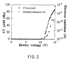
- Figure 2 shows the yield of Cl - ions desorbed from the outer surface of a metal-insulator-metal (MIM) device on which chloroform, CCl 3 H, is adsorbed by exposing the device to a pressure of 10 -8 mbar of CCl 3 H gas admitted to the vacuum chamber housing the device for fifty seconds (an exposure of 0.5 Languirs), as a function of the voltage applied across the device.
- the desorbed ions are detected with a pulse counting mass spectrometer. Also plotted is the current of electrons emitted from the device. It is evident from figure 2:
- Figure 3 gives another example of the device in operation; here pulses of CCl 3 H gas are let into the vacuum chamber housing the device, and the desorbed Cl - signal is recorded as a function of time while the device is running under steady operating conditions.
- the molecular dissociation signal clearly tracks the admitted gas pressure, showing that under these conditions the operation of the device is gas flux limited rather than emission current limited.
Landscapes
- Chemical & Material Sciences (AREA)
- Organic Chemistry (AREA)
- Health & Medical Sciences (AREA)
- General Health & Medical Sciences (AREA)
- Toxicology (AREA)
- Chemical Kinetics & Catalysis (AREA)
- Cold Cathode And The Manufacture (AREA)
- Physical Or Chemical Processes And Apparatus (AREA)
- Organic Low-Molecular-Weight Compounds And Preparation Thereof (AREA)
- Polyoxymethylene Polymers And Polymers With Carbon-To-Carbon Bonds (AREA)
Claims (7)
- Verfahren zur Auslösung eines molekularen Prozesses oder einer molekularen Reaktion in einer Substanz, mit den folgenden Schritten: Inkontaktbringen der Substanz mit einem Kaltkathodenelement und Anlegen eines elektrischen Potentials an das Kaltkathodenelement, um an dessen Oberfläche eine Elektronenemission mit einem für die Auslösung ausreichenden Energieniveau hervorzurufen.
- Verfahren nach Anspruch 1, wobei die Kaltkathode ein Metall-Isolator-Metall-Element (MIM-Element) ist.
- Verfahren nach Anspruch 2, wobei die Isolatorschicht des MIM-Elements eine Dicke von 100 bis 1000 Å aufweist.
- Verfahren nach Anspruch 3, wobei die Isolatorschicht des MIM-Elements eine Dicke von mindestens 200 Å aufweist.
- Verfahren nach einem der Ansprüche 2 bis 4, wobei der elektrische Widerstand der positiv vorgespannten Schicht weniger als 40 Ohm beträgt.
- Verfahren nach einem der Ansprüche 2 bis 5, wobei die Metallschichten des MIM-Elements beide aus Kupfer bestehen und die Isolierschicht ein Siliciumoxid (SiOx) ist.
- Verfahren nach einem der Ansprüche 2 bis 6, das eine molekulare Reaktion mit Chloroform (CCl3H) auslöst.
Applications Claiming Priority (2)
| Application Number | Priority Date | Filing Date | Title |
|---|---|---|---|
| GB9317256 | 1993-08-15 | ||
| GB939317256A GB9317256D0 (en) | 1993-08-19 | 1993-08-19 | Molecular processes and apparatus therefore |
Publications (2)
| Publication Number | Publication Date |
|---|---|
| EP0639401A1 EP0639401A1 (de) | 1995-02-22 |
| EP0639401B1 true EP0639401B1 (de) | 2001-03-28 |
Family
ID=10740732
Family Applications (1)
| Application Number | Title | Priority Date | Filing Date |
|---|---|---|---|
| EP94306029A Expired - Lifetime EP0639401B1 (de) | 1993-08-19 | 1994-08-16 | Verfahren zur Behandlung von Molekülen und Vorrichtung dafür |
Country Status (7)
| Country | Link |
|---|---|
| US (1) | US5608197A (de) |
| EP (1) | EP0639401B1 (de) |
| JP (1) | JP3524590B2 (de) |
| AT (1) | ATE200036T1 (de) |
| DE (1) | DE69426955T2 (de) |
| ES (1) | ES2156138T3 (de) |
| GB (1) | GB9317256D0 (de) |
Families Citing this family (4)
| Publication number | Priority date | Publication date | Assignee | Title |
|---|---|---|---|---|
| DE19616206A1 (de) * | 1996-04-23 | 1997-11-13 | Fraunhofer Ges Forschung | Vorrichtung zur Nachbehandlung von Abgas durch Kombination von Gasentladung und Katalysator |
| JP2003512153A (ja) * | 1999-10-20 | 2003-04-02 | ネオキスメット エルエルシー | 固体表面触媒反応装置 |
| JP4442203B2 (ja) * | 2003-11-25 | 2010-03-31 | パナソニック電工株式会社 | 電子線放射装置 |
| US7898160B2 (en) * | 2003-11-25 | 2011-03-01 | Panasonic Electric Works Co., Ltd. | Method and apparatus for modifying object with electrons generated from cold cathode electron emitter |
Family Cites Families (9)
| Publication number | Priority date | Publication date | Assignee | Title |
|---|---|---|---|---|
| BE633414A (de) * | 1962-06-18 | 1900-01-01 | ||
| US3836786A (en) * | 1967-01-04 | 1974-09-17 | Purification Sciences Inc | Dielectric liquid-immersed corona generator |
| US3772172A (en) * | 1971-10-29 | 1973-11-13 | R Zhagatspanian | Method of removing hydrogen from chlorine gas |
| US4195606A (en) * | 1977-11-17 | 1980-04-01 | Pearson Asa M | Method and apparatus for treating air for internal combustion engines |
| US4204926A (en) * | 1979-03-16 | 1980-05-27 | The United States Of America As Represented By The Secretary Of The Army | Method for the removal of phosgene impurities from boron trichloride |
| US5201681A (en) * | 1987-02-06 | 1993-04-13 | Canon Kabushiki Kaisha | Method of emitting electrons |
| WO1989002868A1 (en) * | 1987-09-28 | 1989-04-06 | Sackinger William M | Electrical device for conversion of molecular weights |
| US5059292A (en) * | 1989-02-28 | 1991-10-22 | Collins George J | Single-chamber apparatus for in-situ generation of dangerous polyatomic gases and radicals from a source material contained within a porous foamed structure |
| US5019530A (en) * | 1990-04-20 | 1991-05-28 | International Business Machines Corporation | Method of making metal-insulator-metal junction structures with adjustable barrier heights |
-
1993
- 1993-08-19 GB GB939317256A patent/GB9317256D0/en active Pending
-
1994
- 1994-08-11 US US08/289,151 patent/US5608197A/en not_active Expired - Fee Related
- 1994-08-16 AT AT94306029T patent/ATE200036T1/de not_active IP Right Cessation
- 1994-08-16 EP EP94306029A patent/EP0639401B1/de not_active Expired - Lifetime
- 1994-08-16 DE DE69426955T patent/DE69426955T2/de not_active Expired - Fee Related
- 1994-08-16 ES ES94306029T patent/ES2156138T3/es not_active Expired - Lifetime
- 1994-08-19 JP JP19515794A patent/JP3524590B2/ja not_active Expired - Fee Related
Also Published As
| Publication number | Publication date |
|---|---|
| DE69426955D1 (de) | 2001-05-03 |
| JPH07171382A (ja) | 1995-07-11 |
| DE69426955T2 (de) | 2001-08-23 |
| EP0639401A1 (de) | 1995-02-22 |
| US5608197A (en) | 1997-03-04 |
| JP3524590B2 (ja) | 2004-05-10 |
| GB9317256D0 (en) | 1993-10-06 |
| ATE200036T1 (de) | 2001-04-15 |
| ES2156138T3 (es) | 2001-06-16 |
Similar Documents
| Publication | Publication Date | Title |
|---|---|---|
| Coburn et al. | Glow‐discharge mass spectrometry—Technique for determining elemental composition profiles in solids | |
| Pennebaker | RF sputtered strontium titanate films | |
| Jones et al. | Surface films and field emission of electrons | |
| Biederman | Metal-insulator-metal sandwich structures with anomalous properties | |
| Hüfner et al. | X-ray photoemission spectra of palladium | |
| US6583578B1 (en) | Field emission-type electron source and manufacturing method thereof | |
| US6540898B2 (en) | Method and system for manufacture of field emission display | |
| US7304299B2 (en) | Super alloy ionization chamber for reactive samples | |
| US5608197A (en) | Molecular processes and apparatus | |
| Schmidt et al. | Electronic structure of oligorylenes in thin solid films | |
| Rudmann et al. | Prevention of the cathode induced electrochemical degradation of [Ru (bpy) 3](PF 6) 2 light emitting devices | |
| Baun | Characterization of tungsten impregnated dispenser cathodes using ISS and SIMS | |
| Clavilier et al. | The use of auger electron spectroscopy for the characterisation of the surfaces of spherical gold electrodes | |
| Umemoto et al. | The behavior of surface oxide film on ruthenium and rhodium plated contacts | |
| Lamartine et al. | AES-RGA investigations of various types of cathodes during activation in ultrahigh vacuum | |
| Ross et al. | Liquid metal substrate for dynamic secondary ion mass spectrometry | |
| Bernhard | Work function study of iridium oxide and molybdenum using UPS and simultaneous Fowler-Nordheim IV plots with field emission energy distributions | |
| Venkatasubramanian et al. | Studies of multiple ionization in the RF spark and vacuum vibrator arc ion sources | |
| Lamartine et al. | Application of low damage SIMS/AES/XPS of the Ba-OW system to cathode characterization | |
| Tantraporn | A New Technique for the Study of Electronic Transport in Insulators | |
| JPH0691185B2 (ja) | 無機誘電薄層の形成方法 | |
| Chalamala | The physics of gaseous exposures on active field emission microcathode arrays | |
| RU2271053C2 (ru) | Полевой эмиссионный катод и способы его изготовления (варианты) | |
| Verhoeven | Atomically Clean Surfaces | |
| Gray et al. | ThO2 on Ir Cathodes for Electron Bombarded Semiconductor Devices |
Legal Events
| Date | Code | Title | Description |
|---|---|---|---|
| PUAI | Public reference made under article 153(3) epc to a published international application that has entered the european phase |
Free format text: ORIGINAL CODE: 0009012 |
|
| AK | Designated contracting states |
Kind code of ref document: A1 Designated state(s): AT BE CH DE ES FR GB IE IT LI NL SE |
|
| 17P | Request for examination filed |
Effective date: 19950725 |
|
| 17Q | First examination report despatched |
Effective date: 19970530 |
|
| GRAG | Despatch of communication of intention to grant |
Free format text: ORIGINAL CODE: EPIDOS AGRA |
|
| RAP1 | Party data changed (applicant data changed or rights of an application transferred) |
Owner name: THE UNIVERSITY OF BIRMINGHAM |
|
| GRAG | Despatch of communication of intention to grant |
Free format text: ORIGINAL CODE: EPIDOS AGRA |
|
| GRAH | Despatch of communication of intention to grant a patent |
Free format text: ORIGINAL CODE: EPIDOS IGRA |
|
| GRAH | Despatch of communication of intention to grant a patent |
Free format text: ORIGINAL CODE: EPIDOS IGRA |
|
| GRAA | (expected) grant |
Free format text: ORIGINAL CODE: 0009210 |
|
| AK | Designated contracting states |
Kind code of ref document: B1 Designated state(s): AT BE CH DE ES FR GB IE IT LI NL SE |
|
| REF | Corresponds to: |
Ref document number: 200036 Country of ref document: AT Date of ref document: 20010415 Kind code of ref document: T |
|
| REG | Reference to a national code |
Ref country code: CH Ref legal event code: NV Representative=s name: E. BLUM & CO. PATENTANWAELTE Ref country code: CH Ref legal event code: EP |
|
| ITF | It: translation for a ep patent filed | ||
| REG | Reference to a national code |
Ref country code: IE Ref legal event code: FG4D |
|
| REF | Corresponds to: |
Ref document number: 69426955 Country of ref document: DE Date of ref document: 20010503 |
|
| ET | Fr: translation filed | ||
| REG | Reference to a national code |
Ref country code: ES Ref legal event code: FG2A Ref document number: 2156138 Country of ref document: ES Kind code of ref document: T3 |
|
| PGFP | Annual fee paid to national office [announced via postgrant information from national office to epo] |
Ref country code: SE Payment date: 20010807 Year of fee payment: 8 |
|
| PGFP | Annual fee paid to national office [announced via postgrant information from national office to epo] |
Ref country code: AT Payment date: 20010813 Year of fee payment: 8 |
|
| PGFP | Annual fee paid to national office [announced via postgrant information from national office to epo] |
Ref country code: CH Payment date: 20010815 Year of fee payment: 8 |
|
| PGFP | Annual fee paid to national office [announced via postgrant information from national office to epo] |
Ref country code: NL Payment date: 20010830 Year of fee payment: 8 |
|
| PGFP | Annual fee paid to national office [announced via postgrant information from national office to epo] |
Ref country code: BE Payment date: 20010927 Year of fee payment: 8 |
|
| REG | Reference to a national code |
Ref country code: GB Ref legal event code: IF02 |
|
| PLBE | No opposition filed within time limit |
Free format text: ORIGINAL CODE: 0009261 |
|
| STAA | Information on the status of an ep patent application or granted ep patent |
Free format text: STATUS: NO OPPOSITION FILED WITHIN TIME LIMIT |
|
| 26N | No opposition filed | ||
| REG | Reference to a national code |
Ref country code: GB Ref legal event code: 732E |
|
| PGFP | Annual fee paid to national office [announced via postgrant information from national office to epo] |
Ref country code: GB Payment date: 20020814 Year of fee payment: 9 |
|
| PG25 | Lapsed in a contracting state [announced via postgrant information from national office to epo] |
Ref country code: AT Free format text: LAPSE BECAUSE OF NON-PAYMENT OF DUE FEES Effective date: 20020816 |
|
| PG25 | Lapsed in a contracting state [announced via postgrant information from national office to epo] |
Ref country code: SE Free format text: LAPSE BECAUSE OF NON-PAYMENT OF DUE FEES Effective date: 20020817 |
|
| PGFP | Annual fee paid to national office [announced via postgrant information from national office to epo] |
Ref country code: ES Payment date: 20020826 Year of fee payment: 9 |
|
| PG25 | Lapsed in a contracting state [announced via postgrant information from national office to epo] |
Ref country code: LI Free format text: LAPSE BECAUSE OF NON-PAYMENT OF DUE FEES Effective date: 20020831 Ref country code: CH Free format text: LAPSE BECAUSE OF NON-PAYMENT OF DUE FEES Effective date: 20020831 Ref country code: BE Free format text: LAPSE BECAUSE OF NON-PAYMENT OF DUE FEES Effective date: 20020831 |
|
| BERE | Be: lapsed |
Owner name: THE *UNIVERSITY OF BIRMINGHAM Effective date: 20020831 |
|
| PG25 | Lapsed in a contracting state [announced via postgrant information from national office to epo] |
Ref country code: NL Free format text: LAPSE BECAUSE OF NON-PAYMENT OF DUE FEES Effective date: 20030301 |
|
| EUG | Se: european patent has lapsed | ||
| REG | Reference to a national code |
Ref country code: CH Ref legal event code: PL |
|
| NLV4 | Nl: lapsed or anulled due to non-payment of the annual fee |
Effective date: 20030301 |
|
| PG25 | Lapsed in a contracting state [announced via postgrant information from national office to epo] |
Ref country code: GB Free format text: LAPSE BECAUSE OF NON-PAYMENT OF DUE FEES Effective date: 20030816 |
|
| PG25 | Lapsed in a contracting state [announced via postgrant information from national office to epo] |
Ref country code: ES Free format text: LAPSE BECAUSE OF NON-PAYMENT OF DUE FEES Effective date: 20030818 |
|
| PGFP | Annual fee paid to national office [announced via postgrant information from national office to epo] |
Ref country code: DE Payment date: 20040226 Year of fee payment: 10 |
|
| GBPC | Gb: european patent ceased through non-payment of renewal fee |
Effective date: 20030816 |
|
| REG | Reference to a national code |
Ref country code: ES Ref legal event code: FD2A Effective date: 20030818 |
|
| PG25 | Lapsed in a contracting state [announced via postgrant information from national office to epo] |
Ref country code: DE Free format text: LAPSE BECAUSE OF NON-PAYMENT OF DUE FEES Effective date: 20050301 |
|
| PGFP | Annual fee paid to national office [announced via postgrant information from national office to epo] |
Ref country code: FR Payment date: 20050809 Year of fee payment: 12 |
|
| PGFP | Annual fee paid to national office [announced via postgrant information from national office to epo] |
Ref country code: IE Payment date: 20050811 Year of fee payment: 12 |
|
| PG25 | Lapsed in a contracting state [announced via postgrant information from national office to epo] |
Ref country code: IE Free format text: LAPSE BECAUSE OF NON-PAYMENT OF DUE FEES Effective date: 20060816 |
|
| PGFP | Annual fee paid to national office [announced via postgrant information from national office to epo] |
Ref country code: IT Payment date: 20060831 Year of fee payment: 13 |
|
| REG | Reference to a national code |
Ref country code: IE Ref legal event code: MM4A |
|
| REG | Reference to a national code |
Ref country code: FR Ref legal event code: ST Effective date: 20070430 |
|
| PG25 | Lapsed in a contracting state [announced via postgrant information from national office to epo] |
Ref country code: FR Free format text: LAPSE BECAUSE OF NON-PAYMENT OF DUE FEES Effective date: 20060831 |
|
| PG25 | Lapsed in a contracting state [announced via postgrant information from national office to epo] |
Ref country code: IT Free format text: LAPSE BECAUSE OF NON-PAYMENT OF DUE FEES Effective date: 20070816 |