EP0639914A2 - Procédé d'acquisition et asservissement de phase pour signaux "MSK" - Google Patents
Procédé d'acquisition et asservissement de phase pour signaux "MSK" Download PDFInfo
- Publication number
- EP0639914A2 EP0639914A2 EP94303787A EP94303787A EP0639914A2 EP 0639914 A2 EP0639914 A2 EP 0639914A2 EP 94303787 A EP94303787 A EP 94303787A EP 94303787 A EP94303787 A EP 94303787A EP 0639914 A2 EP0639914 A2 EP 0639914A2
- Authority
- EP
- European Patent Office
- Prior art keywords
- bit
- phase
- word
- preamble
- signal
- Prior art date
- Legal status (The legal status is an assumption and is not a legal conclusion. Google has not performed a legal analysis and makes no representation as to the accuracy of the status listed.)
- Granted
Links
Images

Classifications
-
- H—ELECTRICITY
- H04—ELECTRIC COMMUNICATION TECHNIQUE
- H04L—TRANSMISSION OF DIGITAL INFORMATION, e.g. TELEGRAPHIC COMMUNICATION
- H04L27/00—Modulated-carrier systems
- H04L27/18—Phase-modulated carrier systems, i.e. using phase-shift keying
- H04L27/22—Demodulator circuits; Receiver circuits
- H04L27/233—Demodulator circuits; Receiver circuits using non-coherent demodulation
- H04L27/2338—Demodulator circuits; Receiver circuits using non-coherent demodulation using sampling
Definitions
- This invention relates to an arrangement for reducing the lock-up time and improving the noise performance in a receiver for burst minimum-shift-keyed communications.
- MSK Minimum-shift keying
- Hz hertz
- MSK signals are demodulated by concurrent use of in-phase (I) and quadrature (Q) demodulators, each of which includes the multiplier.
- Sinusoidal and co-sinusoidal reference or demodulating signals are applied to the Q and I multipliers, respectively, at a frequency which is ideally equal to that of the carrier frequency of the MSK signal.
- Asynchronous demodulation can be accomplished with reference signals which are at the same frequency as the MSK carrier, but which are not necessarily in the same phase. This type of asynchronous demodulation results in an increase in noise by comparison with synchronous demodulation, in which the sinusoidal reference signal is in both frequency and phase synchronism with a carrier component of the modulated MSK signal. Increased noise results in increased error rate, and is therefore undesirable.
- the MSK signal to be received may be downconverted to baseband in preparation for demodulation.
- the downconversion is performed by mixing or multiplying a local oscillator signal with the MSK-modulated carrier. If the local oscillator signal is not phase coherent with the MSK carrier, the baseband signal carrier will include a phase drift or phase error. This phase error results in increased noise in the demodulated signal and increases the bit error rate (BER).
- BER bit error rate
- An MSK receiver includes a downconverter for downconverting the received MSK signals.
- the phase drift or phase error per bit of the message preamble is determined.
- the reference carriers are generated, and the phase of the reference signals is adjusted during message demodulation under the control of the rate of phase change per bit across the preamble portion.
- the downconverted MSK signal burst is digitized and the digitized burst signal is stored in memory, following which it is read repeatedly so that bit timing, start-of-message timing, carrier phase, and carrier drift processing may be performed in a desired sequence, using all the available information for more accurate demodulation.
- a second order tracking loop produces the demodulation reference signals. In one embodiment, this is accomplished by determining the difference between the estimated signal phases of the two bits preceding the current bit, and subtracting from the difference the estimated phase change per bit.
- FIGURE 1 illustrates a transmitter designated generally as 10 including a source of digital information 12, which applies the information over a data path 14 to a control apparatus illustrated as a block 16, and to the common element of a single-pole, double-throw switch 18 illustrated by mechanical switch symbol.
- a control apparatus illustrated as a block 16
- switch 18 alternates positions, under the control of controller 16, to connect source 12 by way of a data path 20a to a memory 22a in the illustrated position of the switch, and in the other position (not illustrated) by way of data path 20b to a memory 22b.
- source 12 produces a stream of digital information which is controlled, in conjunction with controller 16, so that sequential bursts of information are applied alternately to memories 22a and 22b for storage.
- a further single-pole, double-throw switch 24 is also controlled by controller 16, and couples the outputs of memories of 22a and 22b by way of a data path 26 to an error coding block illustrated as 28.
- Switch 24 is controlled in conjunction with switch 18 so that the memories 22a and 22b are written into and read alternately, in a fashion known as "ping-pong".
- controller 16 In the illustrated position of switch 24, memory 22b is being read under control of controller 16, and the burst of data information stored therein is applied to error coding block 28, which encodes the data and applies it to a time-division multiplex (MPX) block 30.
- Controller 16 also controls a preamble generator 32 which generates a predetermined preamble in association with each burst of information data.
- Multiplex block 30 combines the preamble and coded information data, and applies the multiplexed signals over a data path 34 to an MSK modulator 36.
- MSK modulator 36 modulates the signals onto a carrier.
- the modulated MSK signals including MSK symbols representative of the preamble and information data, are applied over a path 38 to an upconverter 40, which upconverts the frequency of the modulated signal to a frequency established by the frequency of local oscillator 42.
- the upconverted signal is applied from upconverter 40 to an antenna 44, which transmits the signal, as suggested by an arrow 46.
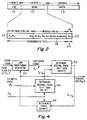
- FIGURE 2 illustrates the relationship of the preamble to the information data at the output of MSK modulator 36 of FIGURE 1 in a particular embodiment of the invention.
- a first portion of the preamble is a continuous-wave (CW) portion 210 having a duration equal to 108 bits.
- CW portion 210 a start-of-message (SOM) portion 212 has a duration of 216 bits.
- the information data portion 214 has a length which may be fixed or variable as the information burst length may require.
- start-of-message portion 212 includes a bit/word sync portion 216 having a duration of 20 words, followed by a message sync portion 218 having a duration of 9 words.
- the start-of-message portion also includes an order wire (OW) portion 220, which is not particularly related to the invention, and which may be considered to be a portion of the information signal.
- OW order wire
- Each word of bit/word sync portion 216 and message sync portion 218 of the preamble has seven bits, so that the bit/word sync portion and message sync portion together represent 29 words, each of which is a sequence of 7 bits, for a total of 203 bits.
- Each of the 20 words of bit/word sync portion 216 of the preamble of FIGURE 2 is the same word, designated A o .
- the bits of each of the words of bit/word sync portion 216 are selected for low autocorrelation as, for example, by use of a Barker sequence.
- the words of the message sync portion 218 are selected from among cyclic shifts of the 7-bit Barker sequence A4, A2, A5, A3, A5, A2, A4, A0, A0, where A i is A0 cyclically shifted to the left by i bits.
- A2 equals 1-1-11-111.
- FIGURE 3 is a simplified block diagram, designated as 310, of a receiver in accordance with the invention.
- transmitted signals 46 are received by an antenna 344.
- the received signals can be represented as where T is the channel bit duration, f c is the carrier frequency, ⁇ is the unknown signal phase, A I (t) and A Q (t) are the even and odd transmitted bit sequences, respectively.
- the quantity n(t) is the received noise process, which is usually modelled as an additive white Gaussian noise (AWGN) with single-sided spectral density N0.
- AWGN additive white Gaussian noise
- the received signals are applied to a downconverter 340, which receives in-phase (I) and quadrature (Q) components of local oscillator signals from a local oscillator 342. Since local oscillator 342 is different from local oscillator 42 of FIGURE 1, is in a different environment, and is supplied with energizing voltage from a different source, its frequency will, in general, be different from the frequency of local oscillator 42.
- the downconverted signal produced on signal path 312 by downconverter 340 therefore, causes the MSK carrier to include a phase drift or phase error component.
- the downconverter generates the in-phase baseband analog signals, represented as and the quadrature baseband analog signals, represented as where ⁇ f is the error in estimating the carrier frequency, and LPF denotes low-pass filtering, which removes high-frequency terms or components.
- the downconverted x(t) and y(t) burst signals are applied from data path 312 to an analog-to-digital converter (ADC) 314, which samples the incoming signal, and produces digital signal samples at a rate of at least two, and preferably four or more, digital samples per bit of the incoming signal. Four samples per bit corresponds to eight samples per MSK symbol.
- ADC analog-to-digital converter
- the sampled, digitized signal is applied from ADC 314 over a data path 316 to a memory (RAM) 318 in which the entire burst signal, including the start-of-message portion of the preamble and the information data, are stored.
- the CW portion of the preamble is applied directly to a frequency acquisition apparatus illustrated as 320, which adjusts the frequency of local oscillator 342 toward the frequency of the received carrier.
- RAM 318 and frequency acquisition block 320 are part of a preamble processing arrangement 328.
- the frequency of local oscillator 342 cannot be adjusted to be identical to the frequency of the received signal.
- the effective phase of the MSK carrier will include a phase progression component.
- the information stored in memory 318 of FIGURE 3 includes the effect of this time-varying phase error.
- a timing acquisition block 322 is coupled to RAM 318 and to a ROM memory 326 in FIGURE 3.
- ROM 326 is preloaded with information equivalent to a replica of start-of-message portion 212 of the preamble of FIGURE 2, including all twenty-nine sequences of seven bits each of the bit/word sync portion 216 and message sync portion 218:
- Bit/word timing block 322 compares the bit/word sync portion of the received message from RAM memory 318, as described below, with the stored information from ROM memory 326.
- phase change estimation block illustrated as 324, in which stored copies of the received information from RAM 318 are further compared with stored replicas of the preamble from ROM 326, to determine or form an estimate of (a) the phase of the MSK carrier at the beginning of the start-of-message portion of the received signal, and (b) the phase change per bit across the preamble of the message, or more particularly across the bit/word sync and the message sync portions of the preamble.
- the resulting phase information is applied over a data path 329 to a phase tracking block 330, which combines the beginning-of-SOM phase with the phase-change-per-bit information to produce a demodulation carrier.
- the demodulation carrier is applied to a coherent MSK demodulator 332 together with stored data. Bit decisions are made in demodulator 332, which are applied back to phase tracking block 330 to allow data direction of the MSK carrier phase. The results of demodulation are also applied to a decoder block 334 for further processing.
- FIGURE 3 illustrates discrete processor blocks such as 322, 324 and 330, these blocks and others may be incorporated into a single software-controlled processor in known manner.
- Block 322 of FIGURE 3 evaluates bit and word timing by repeatedly correlating the stored I and Q samples of the received signal with a replica of one of the 20 identical words of the bit/word synchronization portion of the SOM provided by ROM memory 326.
- the correlation window is advanced in a positive or negative direction by a time period corresponding to one sample interval.
- a total of 28 correlations are performed for each word.
- Each of the 28 correlations of one word is added to the corresponding correlation of the next word. This process of computing 28 correlations and adding to the accumulated correlations continues until a correlation peak can clearly be identified.
- the largest correlation peak indicates the correct bit and word timing to, within one sample interval. While bit and word timing are established by the above-described correlation, the starting time of the SOM is not yet established.
- the starting time of the message synchronization portion 218 of FIGURE 2 can be established. This is accomplished by correlating the stored received message synchronization signal with the stored replica of the message synchronization signal in ROM 326. Since bit/word timing has already been established, the correlations for message sync detection are performed at each word boundary, and the correlation window is advanced by one word at a time.
- the message sync portion of the SOM has nine words, each of seven bits. A message sync correlation is the sum of nine correlations, each seven bits long. The largest value of the message synch correlation peaks identifies the timing of the message synchronization portion.
- the duration of the word/sync portion of the start-of-message is known, so the time of the beginning of the bit/word synchronisation portion is determined, to within one sample interval, by subtracting the known duration of the bit/word synchronization portion from the previously determined starting time of the message sync portion of the start-of-message portion of the preamble.
- phase acquisition and tracking are initiated in block 324 of FIGURE 3 by, in general, estimating the phase change per bit ⁇ b , the signal phase ⁇ , and applying ⁇ b to aid in tracking the signal phase during the SOM portion 212 and the information data portion 214 of the burst communication.
- One frequency synchronization technique gives a frequency error of 0.01/T, where T is the duration of one received bit, at 4 dB signal-to-noise, corresponding to 3.6°/bit.
- the correlation window is advanced at each repetition, but by one bit of the preamble, rather than by one sample interval.
- N is the number of bits in the start-of-message portion 212 and the data portion 214 of FIGURE 2.
- These values are stored in symbol correlation block 319 for use by the phase change estimation block 324, the phase tracking block 324 and the coherent MSK demodulation block 332.
- the symbol correlations for the SOM portion of the preamble are combined coherently over the duration of the 7-bit sequences to form word correlations.
- the word correlation portion is performed by the phase change estimation block 324.
- Block 324 of FIGURE 3 determines Z c and Z s , the unadjusted in-phase and quadrature word correlations, respectively, for each word of the start-of-message portion of the preamble: and where P (M,j) is the j th component of P(M), the factor 8 is the number of samples per MSK symbol.
- Equation (7) represents the sum of products of XCORR multiplied by the MSK symbol pulse polarity for the four even-numbered bits within each word, from which is subtracted the product of YCORR multiplied by the MSK symbol polarity for the three odd-numbered bits in the word.
- the first bit of each word is numbered zero.
- the in-phase and quadrature word correlations R c and R s are related to Z c and Z s .
- sequence of bits corresponding to the second word of bit/word sync portion 210 i.e.
- phase drift per bit ⁇ b is estimated by determining the phase of each 7-bit Barker sequence of a word, taking the difference of the phase estimates of the bit sequences of adjacent words, and averaging all the estimated phase differences.
- Estimated rate of change of phase ⁇ s is unbiased, i.e., not subject to a bias due to the effects of the polarities of adjacent bits. Other choices of start-of-message sequences may result in a bias requiring correction.
- the word 28 is not used since it would introduce a bias in the phase change estimate.
- the estimated value of ⁇ b is applied to phase tracking block 330 of FIGURE 3 to aid in tracking signal phase.
- the initial MSK carrier phase estimate is ⁇ 0 , which is the phase estimate of word 0 computed above in conjunction with the estimation of phase change.
- This phase estimate is refined as described below in conjunction with FIGURE 4 using the start-of-message and a second-order phase tracking loop.
- the estimate of signal phase is incremented (positive or negative) by ⁇ b per bit. Since ⁇ b has an accuracy which may be 0.1° per bit, the MSK carrier signal phase being acquired and tracked changes by at most 0.1° per bit. Such a small uncompensated rate of phase change will allow the loop bandwidth to be reduced to achieve a good phase estimation performance at low SNRs typical of FEC-coded systems.
- the estimated phase change per bit ( ⁇ b ) and the estimated phase of word 0 ( ⁇ 0) are passed from the phase change estimation block 324 over data path 329 to the phase tracking block 330 of FIGURE 3.
- FIGURE 4 is a simplified block diagram of a phase tracking loop in accordance with the invention, which is the phase tracking block 330 of FIGURE 3.
- the XCORR and YCORR values calculated by and stored in the symbol correlation block 319 are applied to an error signal generator 410 together with the estimated signal phase ⁇ k of the current bit.
- Block 410 uses previously determined values of XCORR and YCORR to compute signals r c and r s , which are related to the sine and cosine, respectively, of the phase error ⁇ .
- ⁇ k is the current estimated carrier phase. The bit count starts with 0 for the first bit of the SOM.
- r c and r s are proportional to the cosine and sine, respectively, of the phase error of the unmodulated MSK carrier.
- e tan ⁇ 1 ( r ' s / r ' c ) - ⁇ (15)
- ⁇ is a bias attributable to unequal polarities of the bits, b k-1 and b k+1 , which are next adjacent to the current bit b k .
- the value of the bias term ⁇ can be derived by noting that when r' c is normalized to unity (one), and if the phase error is zero, r' s equals 2/ ⁇ if the current bit b k equals the previous bit b k-1 , and r s ' equals -2/ ⁇ otherwise.
- the error signal e produced by block 410 of FIGURE 4 is limited in magnitude to form e k , the loop error signal where limiting value ⁇ is expressed in radians.
- Generator 410 of FIGURE 4 generates a loop error signal e k for the k th bit as described above.
- the error signals e k are applied from generator 410 to a block 412, together with f k , the residual phase change over one bit.
- the residual phase change over two bits (g k ), which is produced by block 412 of FIGURE 4, is applied to a block 416.
- the value of ⁇ k is applied back to error signal generator 410 for processing as described above in conjunction with block 410, and is also applied to a block 414.
- the loop of FIGURE 4 generates estimated phase signals ⁇ k from the bits of the start-of-message portion of the preamble.
- Phase acquisition begins at bit count 3 of the start-of-message portion of the preamble, because the processing requires knowledge of the phase of the 2 nd preceding, preceding, and following bits, relative to the current bit.
- Phase acquisition ends at bit count 202 of the SOM, which is the last bit for which the value is known a priori.
- the second-order digital loop of FIGURE 4 has an impulse response similar to that of an analog loop with a damping factor 1/ ⁇ 2.
- the noise bandwidth B L of the loop is, for ⁇ 1, B L ⁇ 3 ⁇ /2.
- the loop of FIGURE 4 used to acquire the signal phase from the preamble is also used for phase tracking during the information data portion of the message.
- the advantage of using the same tracking loop is that the loop has already reached steady-state operation before data demodulation begins.
- the transmitted bits are not known a priori. Consequently, decision-directed tracking is employed in blocks 330 and 332 of FIGURE 3, in conjunction with the loop of FIGURE 4.
- the decision-directed tracking is identical to the tracking described above with the exception that b k-1 , b k and b k+1 are demodulated bit values instead of known bit values. A decision must be made whether an information data bit is 1 or -1.
- the bit decisions are performed by coherent MSK demodulation block 332.
- the decision rule for bit modulation or polarity b k is An initial bit decision for the next following bit, b k+1 , is made by using ⁇ k + ⁇ b in place of ⁇ k in equations 21 and 22, and the initial bit decision is redetermined when the new phase estimate is available.
- bit/word sync processing can begin almost immediately after the beginning of reception, and need not wait for reception and storage of the data portion of the MSK burst, nor even for completion of the reception and storage of the preamble.
- the carrier phase can be acquired before reception of the message portion of the burst is completed. Demodulation can therefore begin on the earlier-received portions of the message data before reception of the message portion is completed.
- the demodulation rate is not limited by the rate of data reception, but by the processor speed, which is likely to be much greater. The demodulation can therefore "catch up" with the data, and demodulation may be completed essentially concurrently with the end of the message data.
Landscapes
- Engineering & Computer Science (AREA)
- Computer Networks & Wireless Communication (AREA)
- Signal Processing (AREA)
- Synchronisation In Digital Transmission Systems (AREA)
- Digital Transmission Methods That Use Modulated Carrier Waves (AREA)
Applications Claiming Priority (2)
| Application Number | Priority Date | Filing Date | Title |
|---|---|---|---|
| US98590 | 1979-11-29 | ||
| US08/098,590 US5425058A (en) | 1993-07-28 | 1993-07-28 | MSK phase acquisition and tracking method |
Publications (3)
| Publication Number | Publication Date |
|---|---|
| EP0639914A2 true EP0639914A2 (fr) | 1995-02-22 |
| EP0639914A3 EP0639914A3 (fr) | 1995-04-19 |
| EP0639914B1 EP0639914B1 (fr) | 1999-12-29 |
Family
ID=22270019
Family Applications (1)
| Application Number | Title | Priority Date | Filing Date |
|---|---|---|---|
| EP94303787A Expired - Lifetime EP0639914B1 (fr) | 1993-07-28 | 1994-05-26 | Procédé d'acquisition et asservissement de phase pour signaux "MSK" |
Country Status (5)
| Country | Link |
|---|---|
| US (1) | US5425058A (fr) |
| EP (1) | EP0639914B1 (fr) |
| JP (1) | JPH07154436A (fr) |
| CA (1) | CA2124491A1 (fr) |
| DE (1) | DE69422350T2 (fr) |
Cited By (7)
| Publication number | Priority date | Publication date | Assignee | Title |
|---|---|---|---|---|
| WO1996034481A3 (fr) * | 1995-04-28 | 1996-11-28 | Ionica Int Ltd | Filtre adaptatif a utiliser dans un recepteur mrt/amrt |
| EP0748124A3 (fr) * | 1995-06-07 | 1999-05-06 | Discovision Associates | Appareil et méthode de traitement de signal |
| EP0814586A3 (fr) * | 1996-06-18 | 2000-12-27 | Japan Radio Co., Ltd | Synchronisation de trame, d'horloge, de fréquence et de phase, par l'utilisation d'un mot unique |
| WO2001028146A1 (fr) * | 1999-10-12 | 2001-04-19 | Itran Communications Ltd. | Appareil et procede de synchronisation adaptative dans un recepteur de communications a spectre etale |
| US6658242B1 (en) * | 1997-12-12 | 2003-12-02 | Thomson Licensing S.A. | TDMA wireless telephone system with independently tracked demodulation parameters |
| US7292665B2 (en) | 2004-12-16 | 2007-11-06 | Genesis Microchip Inc. | Method and apparatus for reception of data over digital transmission link |
| CN104168240A (zh) * | 2014-07-18 | 2014-11-26 | 成都天奥信息科技有限公司 | 一种oqpsk突发信号的多路并行同步解调方法 |
Families Citing this family (21)
| Publication number | Priority date | Publication date | Assignee | Title |
|---|---|---|---|---|
| US8352400B2 (en) | 1991-12-23 | 2013-01-08 | Hoffberg Steven M | Adaptive pattern recognition based controller apparatus and method and human-factored interface therefore |
| US10361802B1 (en) | 1999-02-01 | 2019-07-23 | Blanding Hovenweep, Llc | Adaptive pattern recognition based control system and method |
| US5583890A (en) * | 1994-09-19 | 1996-12-10 | Motorola, Inc. | Error correction of MSK signals dependent on sample quality |
| JP3310160B2 (ja) * | 1996-03-29 | 2002-07-29 | 松下電器産業株式会社 | スペクトラム拡散方式受信装置 |
| US5982811A (en) * | 1996-07-12 | 1999-11-09 | General Electric Company | Method for efficient sampling in a correlator |
| GB9617598D0 (en) * | 1996-08-22 | 1996-10-02 | Philips Electronics Nv | M-ary fsk receiver |
| US6104767A (en) * | 1997-11-17 | 2000-08-15 | Telefonaktiebolaget Lm Ericsson | Method and apparatus for estimating a frequency offset |
| US6515976B1 (en) * | 1998-04-06 | 2003-02-04 | Ericsson Inc. | Demodulation method and apparatus in high-speed time division multiplexed packet data transmission |
| US7966078B2 (en) | 1999-02-01 | 2011-06-21 | Steven Hoffberg | Network media appliance system and method |
| US8648692B2 (en) | 1999-07-23 | 2014-02-11 | Seong Sang Investments Llc | Accessing an automobile with a transponder |
| US6647270B1 (en) * | 1999-09-10 | 2003-11-11 | Richard B. Himmelstein | Vehicletalk |
| US6934327B1 (en) * | 2001-04-23 | 2005-08-23 | Rockwell Collins | Acquisition of a continuous-phase modulation waveform |
| US20190362725A1 (en) | 2005-08-17 | 2019-11-28 | Tamiras Per Pte. Ltd., Llc | Providing access with a portable device and voice commands |
| JP2011101131A (ja) * | 2009-11-05 | 2011-05-19 | Nec Corp | バースト通信用変調装置、復調装置、変調および復調方法ならびに通信システム |
| US8102302B2 (en) * | 2010-05-20 | 2012-01-24 | Northrop Grumman Guidance & Electronics Company, Inc. | Mode 5 detection process using phase and amplitude correlation |
| US8325433B2 (en) * | 2011-01-19 | 2012-12-04 | Lsi Corporation | Systems and methods for reduced format data processing |
| JP5606411B2 (ja) * | 2011-08-26 | 2014-10-15 | 三菱電機株式会社 | 無線信号同期処理装置 |
| GB2523108A (en) * | 2014-02-12 | 2015-08-19 | Canon Kk | Frame synchronization at low ADC resolution |
| WO2015125194A1 (fr) * | 2014-02-21 | 2015-08-27 | パナソニック インテレクチュアル プロパティ コーポレーション オブ アメリカ | Appareil d'émission, appareil de réception, procédé d'émission et procédé de réception |
| ES3008934T3 (en) * | 2018-04-16 | 2025-03-25 | Lg Electronics Inc | Apparatus and method for performing transmission of data stream in wireless power transmission system |
| US12483455B2 (en) * | 2021-03-16 | 2025-11-25 | Telefonaktiebolaget Lm Ericsson (Publ) | Transmitting data or determining a frequency and timing estimate of a received signal |
Family Cites Families (10)
| Publication number | Priority date | Publication date | Assignee | Title |
|---|---|---|---|---|
| US4518996A (en) * | 1983-03-21 | 1985-05-21 | Rca Corporation | Synchronization system that uses all valid signals |
| US4599732A (en) * | 1984-04-17 | 1986-07-08 | Harris Corporation | Technique for acquiring timing and frequency synchronization for modem utilizing known (non-data) symbols as part of their normal transmitted data format |
| US4583048A (en) * | 1985-02-26 | 1986-04-15 | Rca Corporation | MSK digital demodulator for burst communications |
| US4635279A (en) * | 1985-07-25 | 1987-01-06 | Rca Corporation | Arrangement for coherently generating sinusoids of different frequencies, and angle modulation data receiver using the arrangement |
| US4694467A (en) * | 1986-07-03 | 1987-09-15 | Signatron, Inc. | Modem for use in multipath communication systems |
| FR2633471B1 (fr) * | 1988-06-28 | 1990-10-05 | Trt Telecom Radio Electr | Procede de demodulation coherente d'un signal module numeriquement en phase continue et a enveloppe constante |
| CA2018855C (fr) * | 1989-06-14 | 1993-09-21 | Shousei Yoshida | Demodulateur de salves a circuits d'extraction de porteuses et de signaux d'horloge incorpores a une sequence de symboles alternatifs |
| US5241545A (en) * | 1990-11-14 | 1993-08-31 | Motorola, Inc. | Apparatus and method for recovering a time-varying signal using multiple sampling points |
| KR950003666B1 (ko) * | 1990-12-31 | 1995-04-17 | 삼성전자 주식회사 | 지엠에스케이신호복조방법 및 그 장치 |
| US5195108A (en) * | 1991-09-30 | 1993-03-16 | Motorola, Inc. | System and method for determining absolute phase of a differentially-encoded, phase-modulated signal |
-
1993
- 1993-07-28 US US08/098,590 patent/US5425058A/en not_active Expired - Fee Related
-
1994
- 1994-05-26 DE DE69422350T patent/DE69422350T2/de not_active Expired - Fee Related
- 1994-05-26 EP EP94303787A patent/EP0639914B1/fr not_active Expired - Lifetime
- 1994-05-27 CA CA002124491A patent/CA2124491A1/fr not_active Abandoned
- 1994-07-14 JP JP6185395A patent/JPH07154436A/ja active Pending
Cited By (9)
| Publication number | Priority date | Publication date | Assignee | Title |
|---|---|---|---|---|
| WO1996034481A3 (fr) * | 1995-04-28 | 1996-11-28 | Ionica Int Ltd | Filtre adaptatif a utiliser dans un recepteur mrt/amrt |
| EP0748124A3 (fr) * | 1995-06-07 | 1999-05-06 | Discovision Associates | Appareil et méthode de traitement de signal |
| EP0814586A3 (fr) * | 1996-06-18 | 2000-12-27 | Japan Radio Co., Ltd | Synchronisation de trame, d'horloge, de fréquence et de phase, par l'utilisation d'un mot unique |
| US6658242B1 (en) * | 1997-12-12 | 2003-12-02 | Thomson Licensing S.A. | TDMA wireless telephone system with independently tracked demodulation parameters |
| WO2001028146A1 (fr) * | 1999-10-12 | 2001-04-19 | Itran Communications Ltd. | Appareil et procede de synchronisation adaptative dans un recepteur de communications a spectre etale |
| US6614864B1 (en) | 1999-10-12 | 2003-09-02 | Itran Communications Ltd. | Apparatus for and method of adaptive synchronization in a spread spectrum communications receiver |
| US7292665B2 (en) | 2004-12-16 | 2007-11-06 | Genesis Microchip Inc. | Method and apparatus for reception of data over digital transmission link |
| US7412017B2 (en) | 2004-12-16 | 2008-08-12 | Genesis Microchip Inc. | Method and apparatus for reception of data over a transmission link |
| CN104168240A (zh) * | 2014-07-18 | 2014-11-26 | 成都天奥信息科技有限公司 | 一种oqpsk突发信号的多路并行同步解调方法 |
Also Published As
| Publication number | Publication date |
|---|---|
| JPH07154436A (ja) | 1995-06-16 |
| DE69422350D1 (de) | 2000-02-03 |
| EP0639914B1 (fr) | 1999-12-29 |
| CA2124491A1 (fr) | 1995-01-29 |
| DE69422350T2 (de) | 2000-05-11 |
| EP0639914A3 (fr) | 1995-04-19 |
| US5425058A (en) | 1995-06-13 |
Similar Documents
| Publication | Publication Date | Title |
|---|---|---|
| EP0639914B1 (fr) | Procédé d'acquisition et asservissement de phase pour signaux "MSK" | |
| US6226337B1 (en) | Method for the transmission of reference signals in an OFDM system | |
| JP3036750B2 (ja) | 時分割多重アクセス(tdma)無線システム受信機及び該時分割多重アクセス(tdma)無線システム受信機用復調器及び該時分割多重アクセス(tdma)無線システム受信機における多相復調方法 | |
| US4583048A (en) | MSK digital demodulator for burst communications | |
| KR100377257B1 (ko) | 멀티-캐리어 복조 시스템내 정밀 주파수 동기화 방법 및장치 | |
| FI95524B (fi) | Nopea referenssitiedonkeruu ja vaihevirheen kompensointi datan radiolähetystä varten | |
| JP2526931B2 (ja) | Psk信号復調装置 | |
| US4017798A (en) | Spread spectrum demodulator | |
| USRE42538E1 (en) | System and method for signal synchronization in a communication system | |
| US6438173B1 (en) | Multicarrier transmission system for irregular transmission of data blocks | |
| EP0375272B1 (fr) | Démodulateur cohérent pour modulation à déplacements de phase | |
| CA2025232C (fr) | Systeme de restitution de porteuse | |
| EP1278346B1 (fr) | Dispositif de poursuite de phase pour signaux linéairment modulés | |
| EP1794966B1 (fr) | Systeme et procede de recuperation de phase et de frequence de porteuse fondee sur la trame | |
| USRE41607E1 (en) | Data aided symbol timing system for precoded continuous phase modulated signals | |
| US6650187B1 (en) | Decision directed suppressed carrier symbol-rate PLL with programmable phase discriminator and chip-rate phase extrapolation | |
| US6947504B1 (en) | Frequency synchronizer | |
| US4635279A (en) | Arrangement for coherently generating sinusoids of different frequencies, and angle modulation data receiver using the arrangement | |
| US5995536A (en) | System for discrete data transmission with noise-like, broadband signals | |
| EP0573696A1 (fr) | Méthode et système de récupération d'horloge | |
| Classen et al. | An all feedforward synchronization unit for digital radio | |
| US4224575A (en) | Phase/frequency controlled phase shift keyed signal carrier reconstruction circuit | |
| US5546423A (en) | Spread spectrum digital transmission system using low-frequency pseudorandom encoding of the wanted information and spectrum spreading and compression method used in a system of this kind | |
| US5572553A (en) | Digital apparatus for broadband carrier-recovery | |
| US6771713B1 (en) | Data aided carrier phase tracking system for precoded continuous phase modulated signals |
Legal Events
| Date | Code | Title | Description |
|---|---|---|---|
| PUAI | Public reference made under article 153(3) epc to a published international application that has entered the european phase |
Free format text: ORIGINAL CODE: 0009012 |
|
| AK | Designated contracting states |
Kind code of ref document: A2 Designated state(s): DE FR GB IT |
|
| PUAL | Search report despatched |
Free format text: ORIGINAL CODE: 0009013 |
|
| AK | Designated contracting states |
Kind code of ref document: A3 Designated state(s): DE FR GB IT |
|
| 17P | Request for examination filed |
Effective date: 19951019 |
|
| RAP1 | Party data changed (applicant data changed or rights of an application transferred) |
Owner name: LOCKHEED MARTIN CORPORATION |
|
| 17Q | First examination report despatched |
Effective date: 19971119 |
|
| GRAG | Despatch of communication of intention to grant |
Free format text: ORIGINAL CODE: EPIDOS AGRA |
|
| GRAG | Despatch of communication of intention to grant |
Free format text: ORIGINAL CODE: EPIDOS AGRA |
|
| GRAH | Despatch of communication of intention to grant a patent |
Free format text: ORIGINAL CODE: EPIDOS IGRA |
|
| GRAH | Despatch of communication of intention to grant a patent |
Free format text: ORIGINAL CODE: EPIDOS IGRA |
|
| GRAA | (expected) grant |
Free format text: ORIGINAL CODE: 0009210 |
|
| AK | Designated contracting states |
Kind code of ref document: B1 Designated state(s): DE FR GB IT |
|
| ITF | It: translation for a ep patent filed | ||
| REF | Corresponds to: |
Ref document number: 69422350 Country of ref document: DE Date of ref document: 20000203 |
|
| ET | Fr: translation filed | ||
| PLBE | No opposition filed within time limit |
Free format text: ORIGINAL CODE: 0009261 |
|
| STAA | Information on the status of an ep patent application or granted ep patent |
Free format text: STATUS: NO OPPOSITION FILED WITHIN TIME LIMIT |
|
| 26N | No opposition filed | ||
| PGFP | Annual fee paid to national office [announced via postgrant information from national office to epo] |
Ref country code: GB Payment date: 20010427 Year of fee payment: 8 |
|
| PGFP | Annual fee paid to national office [announced via postgrant information from national office to epo] |
Ref country code: FR Payment date: 20010430 Year of fee payment: 8 Ref country code: DE Payment date: 20010430 Year of fee payment: 8 |
|
| REG | Reference to a national code |
Ref country code: GB Ref legal event code: IF02 |
|
| PG25 | Lapsed in a contracting state [announced via postgrant information from national office to epo] |
Ref country code: GB Free format text: LAPSE BECAUSE OF NON-PAYMENT OF DUE FEES Effective date: 20020526 |
|
| PG25 | Lapsed in a contracting state [announced via postgrant information from national office to epo] |
Ref country code: DE Free format text: LAPSE BECAUSE OF NON-PAYMENT OF DUE FEES Effective date: 20021203 |
|
| GBPC | Gb: european patent ceased through non-payment of renewal fee |
Effective date: 20020526 |
|
| PG25 | Lapsed in a contracting state [announced via postgrant information from national office to epo] |
Ref country code: FR Free format text: LAPSE BECAUSE OF NON-PAYMENT OF DUE FEES Effective date: 20030131 |
|
| REG | Reference to a national code |
Ref country code: FR Ref legal event code: ST |
|
| PG25 | Lapsed in a contracting state [announced via postgrant information from national office to epo] |
Ref country code: IT Free format text: LAPSE BECAUSE OF NON-PAYMENT OF DUE FEES;WARNING: LAPSES OF ITALIAN PATENTS WITH EFFECTIVE DATE BEFORE 2007 MAY HAVE OCCURRED AT ANY TIME BEFORE 2007. THE CORRECT EFFECTIVE DATE MAY BE DIFFERENT FROM THE ONE RECORDED. Effective date: 20050526 |