EP0640918A1 - Circuit de mémoire intégré à semi-conducteur - Google Patents
Circuit de mémoire intégré à semi-conducteur Download PDFInfo
- Publication number
- EP0640918A1 EP0640918A1 EP94305470A EP94305470A EP0640918A1 EP 0640918 A1 EP0640918 A1 EP 0640918A1 EP 94305470 A EP94305470 A EP 94305470A EP 94305470 A EP94305470 A EP 94305470A EP 0640918 A1 EP0640918 A1 EP 0640918A1
- Authority
- EP
- European Patent Office
- Prior art keywords
- sector
- redundancy
- redundant
- address
- column
- Prior art date
- Legal status (The legal status is an assumption and is not a legal conclusion. Google has not performed a legal analysis and makes no representation as to the accuracy of the status listed.)
- Granted
Links
- 239000004065 semiconductor Substances 0.000 title claims description 32
- 230000002950 deficient Effects 0.000 claims abstract description 53
- 230000008439 repair process Effects 0.000 claims abstract description 23
- 230000004044 response Effects 0.000 claims description 8
- 230000001419 dependent effect Effects 0.000 claims description 7
- 238000000034 method Methods 0.000 claims description 4
- 238000010586 diagram Methods 0.000 description 34
- 238000012360 testing method Methods 0.000 description 7
- 238000010276 construction Methods 0.000 description 5
- 102100038191 Double-stranded RNA-specific editase 1 Human genes 0.000 description 4
- 101000742223 Homo sapiens Double-stranded RNA-specific editase 1 Proteins 0.000 description 4
- 101000686491 Platymeris rhadamanthus Venom redulysin 1 Proteins 0.000 description 4
- 230000007547 defect Effects 0.000 description 4
- 230000002093 peripheral effect Effects 0.000 description 4
- 230000005540 biological transmission Effects 0.000 description 3
- OCJBOOLMMGQPQU-UHFFFAOYSA-N 1,4-dichlorobenzene Chemical compound ClC1=CC=C(Cl)C=C1 OCJBOOLMMGQPQU-UHFFFAOYSA-N 0.000 description 2
- 230000008901 benefit Effects 0.000 description 2
- 230000003247 decreasing effect Effects 0.000 description 2
- 230000006870 function Effects 0.000 description 2
- 238000004519 manufacturing process Methods 0.000 description 2
- 239000002184 metal Substances 0.000 description 2
- 238000012986 modification Methods 0.000 description 2
- 230000004048 modification Effects 0.000 description 2
- 230000003213 activating effect Effects 0.000 description 1
- 238000003491 array Methods 0.000 description 1
- 238000007599 discharging Methods 0.000 description 1
- 230000017525 heat dissipation Effects 0.000 description 1
- 239000000463 material Substances 0.000 description 1
- 102220030763 rs1385129 Human genes 0.000 description 1
Images


Classifications
-
- G—PHYSICS
- G11—INFORMATION STORAGE
- G11C—STATIC STORES
- G11C29/00—Checking stores for correct operation ; Subsequent repair; Testing stores during standby or offline operation
- G11C29/70—Masking faults in memories by using spares or by reconfiguring
- G11C29/78—Masking faults in memories by using spares or by reconfiguring using programmable devices
- G11C29/80—Masking faults in memories by using spares or by reconfiguring using programmable devices with improved layout
- G11C29/808—Masking faults in memories by using spares or by reconfiguring using programmable devices with improved layout using a flexible replacement scheme
-
- G—PHYSICS
- G11—INFORMATION STORAGE
- G11C—STATIC STORES
- G11C29/00—Checking stores for correct operation ; Subsequent repair; Testing stores during standby or offline operation
- G11C29/70—Masking faults in memories by using spares or by reconfiguring
- G11C29/78—Masking faults in memories by using spares or by reconfiguring using programmable devices
- G11C29/785—Masking faults in memories by using spares or by reconfiguring using programmable devices with redundancy programming schemes
- G11C29/787—Masking faults in memories by using spares or by reconfiguring using programmable devices with redundancy programming schemes using a fuse hierarchy
Definitions
- This invention relates generally to semiconductor integrated circuit memory devices such as floating gate memory devices such as an array of flash electrically erasable programmable read-only memory (EEPROM) cells with redundancy architecture. More particularly, the present invention relates to an improved redundancy architecture for an array of flash EEPROM cells which permit repairing of defective columns of memory cells in the array with spare redundant columns of memory cells on a sector-by-sector basis.
- semiconductor integrated circuit memory devices such as floating gate memory devices such as an array of flash electrically erasable programmable read-only memory (EEPROM) cells with redundancy architecture. More particularly, the present invention relates to an improved redundancy architecture for an array of flash EEPROM cells which permit repairing of defective columns of memory cells in the array with spare redundant columns of memory cells on a sector-by-sector basis.
- EEPROM electrically erasable programmable read-only memory
- semiconductor memory devices are manufactured with a memory array of elements which are accessed by a row decoder and a column decoder to address a particular memory element or row of memory elements in the memory array.
- a sense amplifier is built in the semiconductor chip for sensing the memory state of the selected memory element when addressed by the row decoder and column decoder.
- the density of the memory array on a semiconductor chip has increased to over 1 million memory elements. As the density of the memory array on a semiconductor chip increases, it becomes a significantly more difficult task to produce perfect semiconductor memory chips. In an effort to improve production yields and memory chip reliability, spare or redundant columns of memory cells have been included on the semiconductor chip so as to allow for repairing or replacing defective columns of memory cells in an array.
- the semiconductor memory is generally first tested while it is still in a semiconductor wafer joined with other semiconductor memory chips to determine whether it operates properly. If a faulty area is located, extra memory circuits can then be substituted for the defective elements in this faulty area on the primary memory array of memory elements.
- circuitry is required for selectively deactivating the defective column of memory cells when repair is desired and for activating a redundant column of memory cells to replace the deactivated column.
- the redundant column is required to run the entire length of the array.
- column repair was realized in flash EEPROM arrays only on an array-based redundancy where only one defective column in the entire array could be repaired by the redundant column.
- This sector-based redundancy architecture as will be described is implemented through the use of a plurality of sector select transistors and addressable storage devices.
- a plurality of sector-based redundancy blocks are provided each having redundant columns of memory cells extending through a plurality of sectors.
- the sector select transistors serve to divide the redundant columns into a number of different segments.
- the different segments of the redundant columns residing in the separate sectors are made independent from other segments in the same redundant column and can be thus used to repair a different defective column.
- the addressable storage devices are used for storing sector-based redundant column addresses containing the defective columns of memory cells in the plurality of sectors in association with one of the different redundant column segments to be used in repairing the defective columns in the corresponding ones of the plurality of sectors.
- an improved redundancy architecture for an array of flash EEPROM cells which includes a plurality of sector-based redundancy blocks each having redundant columns of memory cells extending through a plurality of sectors and sector selection means for dividing the redundant columns into different segments residing in the separate sectors so as to allow independent use from other segments in the same redundant columns in repairing defective columns in corresponding ones of the plurality of sectors.
- the present invention is concerned with the provision of a semiconductor integrated circuit memory device having array means formed of a plurality of sectors each formed of an array of flash EEPROM cells and redundancy circuit means for repairing defective columns of memory cells in the plurality of sectors on a sector-by-sector basis.
- the redundancy circuit means includes a plurality of sector-based redundancy blocks each having redundant columns of memory cells extending through the plurality of sectors.
- Sector selection means are provided for dividing the redundant columns into different segments each residing in at least one of the plurality of sectors and for isolating the different segments so as to allow independent use from other segments in the same redundant column in repairing the defective columns in the corresponding ones of the plurality of sectors.
- Addressable fuse storage means are provided for storing redundant column addresses containing the defective columns of memory cells in the plurality of sectors in association with one of the different redundant column segments to be used in repairing the defective columns in the corresponding ones of the plurality of sectors.
- the addressable fuse storage means includes means for programming the redundant column addresses in association with the one of the different redundant column segments.
- the addressable fuse storage means also includes means for reading the stored redundant column address in relation to the plurality of sector-based redundancy blocks and for comparing a selected column address with the stored redundant column address which is being read to generate a redundancy signal and a disable signal when there is a match.
- a redundancy decoder is responsive to the redundancy signal for enabling the redundancy block to be used to repair the defective column.
- a disabling circuit is responsive to the disable signal for disabling a Y-decoder to the defective column.
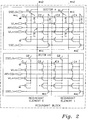
- Figure 1 a chip layout of how the four sector-based redundant blocks 2, 4, 6, and 8 in the sector-based redundancy architecture of the present embodiment are positioned relative to an array 10 of flash EEPROM cells formed of eight sectors 12-26.
- each of the redundant blocks is contained in two corresponding sectors.
- the redundant block 2 resides within the sectors 12 and 14, and the redundant block 4 resides within the sectors 16 and 18.
- the redundant block 6 is contained in the sectors 20 and 22, and the redundant block 8 is contained in the sectors 24 and 26.
- each of the redundant blocks may be contained in any desired number of sectors.
- FIG 2 there is shown a detailed schematic circuit diagram of one of the sector-based redundancy blocks 2-8 of Figure 1. Since each of the redundant blocks 2-8 are identical, it will be sufficient to describe only the redundant block 2.
- the redundant block 2 is used to repair defects in the two sectors 12 and 14.
- the redundant block 2 includes two independent redundant elements (redundant element 0 ⁇ and redundant element 1) each having two sector bit lines bl-0 ⁇ , bl-1 (first level metal--*m1) or equivalently, one array bit line BL0 or BL1 (second level metal--*m2).
- Each second level metal block is located directly over and insulated from the corresponding first level bit line so that the capacitance of the second metal bit line is not significant.
- there are required two independent individual elements in each redundant block so as to cover all single bit line to bit line short conditions.
- Each of the individual sectors 12-26 in the array 10 is isolated from other neighboring sectors through the use of a sector select transistor.
- This technique is described and shown in U.S. Patent No. 5,126,808 to A.J. Montalvo et al. issued on June 30, 1992, and assigned to the same assignee as the present invention, which is hereby incorporated by reference in its entirety.
- sector select transistors Q1, Q2 in the redundant block 2 are used to isolate and allow independent use of the redundant columns C1-C4 residing within the sectors 12 and 14.
- an individual segment residing within the particular sectors can be made independent from other segments in the same columns and can thus be used to replace or repair a different defect.
- This sector-based redundancy architecture is implemented through the use of a plurality of minifuse circuits located in the peripheral area of the chip.
- the plurality of minifuse circuits serve as fuses formed by non-volatile storage elements which are used to enable the redundant elements in the appropriate sector-based redundant blocks as well as to store the sector column addresses (i.e., the address of the defective column in the sectors) to be replaced or repaired by the redundant blocks.
- the minifuse circuits are arrayed in a group of four defining a quad address fuse circuit for sharing a common read path thereby minimizing the number of components and reducing the amount of chip area needed. Further, the minifuse circuits are programmed by a power supply potential VCC in order to eliminate the number of support circuits and thus reducing chip area.
- FIG. 3 there is shown a block diagram of the address CAM periphery architecture of the present invention which is used to implement the sector-based redundancy.
- the address CAM architecture includes a repair select decoder (RED EN DEC) 302, a pretest (PRETEST) 304, fuse select circuits (CAMYSEL) 306a and 306b, read drain decoder (PDCSEL) 308, a reference bias generator circuit (REFBIAS) 310, a gate voltage generator circuit (PDCBRG) 312, addressable fuse storage circuitry (ADBCAMX7) 314a and 314b, a redundancy enable circuit (DISY) 316, redundancy Y-decoders (REDYDEC) 318a, 318b, and a regular column or Y-decoder 318c.
- RED EN DEC repair select decoder
- PRETEST pretest
- CAMYSEL fuse select circuits
- REFBIAS reference bias generator circuit
- ADBCAMX7 addressable fuse storage
- the repair select decoder 302 receives at its inputs a repair signal REP on line 320 and address signals A16, A12 on respective lines 322, 324 and generates an enable programming signal ADDCAMPRG, an enable voltage reference signal REFDEC and an erase signal CAMERSB on respective lines 326, 328 and 330.
- the enable program signal ADDCAMPRG is used to enable programming of the quad address and enable fuse circuits in the addressable fuse storage circuitry (ADDCAMX7) 314a and 314b via the corresponding fuse select circuits 306a and 306b.
- a circuit diagram of the repair select decoder 302 is shown in Figure 4 and is comprised of inverter gates 402-408 and NAND logic gates 410-414.
- the enabling programming signal ADDCAMPRG on the line 326 will be at a high or "1" logic level when the repair signal REP is high and the address signal A12 is low.
- the erase signal CAMERSB on the line 330 will be low when the repair signal REP and the address signals A16, A12 are all high.
- the pretest circuit 404 receives as its inputs a pretest signal PRETEST on line 332 and an address signal A4 on line 334. In response thereto, the pretest circuit generates a first test signal PREB0 ⁇ on line 336 and a second test signal PREB1 on line 338.
- a circuit diagram of the pretest circuit 304 is illustrated in Figure 5 and includes an inverter gate 502 and a pair of NAND logic gates 504, 506. When the signal PRETEST goes high during a pretest mode and the address signal A4 is low, the test signal PREB0 ⁇ will go low and is fed to the redundancy enable circuit 316, which is used to activate the redundant element 0 ⁇ in the redundancy blocks prior to testing them.
- test signal PREB1 when the signal PRETEST goes high during the pretest mode and the address signal A4 is also high, the test signal PREB1 will go low and is fed to the redundancy enable circuit 316 which is used to activate the redundant element 1 in the redundancy blocks prior to testing them.
- the program, erase, and read functions are all active during the pretest mode of operation.
- the fuse select circuit 306a receives as its input the enable programming signal ADDCAMPRG on line 340 and sector address signals A18, A17, and A16B on respective lines 342-346.
- the address A18 is the most significant sector address.
- the address A16B is used to determine which redundant element (0 ⁇ or 1) is selected for programming.
- the read drain decoder circuit (PDCSEL) 308 receives also as its inputs the sector addresses A18 and A17 on lines 350 and 352, respectively.
- a circuit diagram of the read decoder circuit 308 is shown in Figure 7 and is formed by inverter gates 702-712 and NAND logic gates 714-720.
- the addressable fuse storage circuitry 314a receives as its inputs the read select signal PDCSEL(3:0) the reference current signal REFBIAS, the fuse bias signal PDCB, the gate control signal RG, and the sector column address signals A15, A5, A4, A3, A2, A1 and A0 ⁇ on respective lines 356-366. In response thereto, the addressable fuse storage circuitry 314a generates on its output the redundant column select signal YCOMq(6:0) and the redundant column enable signal YCEq on respective lines 368-370.
- the addressable fuse storage circuitry 314a is comprised of seven (7) identical quad address fuse circuits 315a-315g and one (1) quad enable fuse circuit 317. It will be noted that the only difference between the address fuse circuits and the enable fuse circuit is that the supply potential VCC is applied to the address terminal A j rather than the address signal (i.e., A5-A0, A15). Since the fuse circuits 315a-315g and 317 are identical in their construction, it will be sufficient to describe in detail only the fuse circuit 315a. A circuit diagram of the quad address fuse circuit 315a is illustrated in Figure 12.
- the quad address fuse circuit 315a is comprised of four (4) minifuse circuits 319a-319b and a parity circuit 321.
- Each of the four minifuse circuits 319a-319b is used to store one bit address of the full sector-based redundancy column address, corresponding to the location of the defective column in one of the sectors which is to be replaced with one of the different redundant column segments.
- the minifuse circuit 319a stores one of the bit addresses which is associated with the redundant element 0 ⁇ in the redundant block 2
- the minifuse circuit 319b stores one of the bit addresses which is associated with the redundant element 0 ⁇ in the redundant block 4.
- each of the minifuse circuits 319a-319d receives on its input the repair select signals RYSqn, the column address signal A j , the read select signals PDCSELn, a field gate signal FGn, and the gate control signal RG. It will be noted that the output CAMOUT of each minifuse circuit 319a-319d are tied together at node q0 ⁇ so as to share a common read path.
- the parity circuit 321 includes an N-channel pass transistor 323; a P-channel bias transistor 325; inverters 327, 329, and 331; and transmission gates 333, 335.
- the transmission gate 333 is formed by transistors 337 and 339 whose input is at node 341 and whose output is tied to the line 368 for providing the redundant column select signal YCOMqn.
- the transmission gate 335 is formed by transistors 343 and 345 whose input is at node 341a and whose output is also tied to the line 368. If the cell in the minifuse circuit 319a is programmed, which is equivalent to storing a logic "1," the node q0 ⁇ will be at a high level when read by the read select signal PDCSEL0 ⁇ . On the other hand, if the cell in the minifuse circuit 319a is unprogrammed (erased), which is equivalent to storing a logic "0,” the node q0 ⁇ will be at a low level.
- all of the redundant column select signals YCOMq0-YCOMq6 and the enable signal YCEq from the addressable fuse storage circuitry 314a are high or logic "1," one of the redundant elements in the corresponding redundant blocks 2-8 will be enabled for repairing the defective column in the associated sector.
- the redundant element 0 ⁇ in the redundant block 2 would be enabled when there was a match between the stored bit addresses in the minifuse circuits 319a in each of the quad address fuse circuits 315a-315g and the address input signal.
- the fuse bias signal PDCB applied to the gate of the pass transistor 323 is used to protect the drains of the read transistor devices in the minifuse cell from a "drain disturb" during the read mode.
- This fuse bias signal is generated on line 372 by the gate voltage generator circuit 312.
- a detailed schematic circuit diagram of the gate voltage generator circuit 312 is shown in Figure 9.
- the generator circuit 312 also generates a power down repair signal PDREPB on line 374 and the gate control voltage RG on the line 376.
- the circuit 312 receives a discharge signal RECLD on line 378 for discharging the high voltage after programming. This signal is generated by the one-shot generator circuit 380 which is illustrated by the circuit diagram in Figure 10.
- the reference current signal REFBIAS applied to the gate of the transistor 325 functions as a current source so as to supply a reference current in the read operation of the minifuse circuits 319a-319d.
- This reference current signal REFBIAS is generated on line 382 by the reference bias generator 310.
- a schematic circuit diagram of the generator 310 is illustrated in Figure 8.
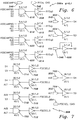
- the minifuse circuit 319a includes a minifuse cell formed of two double poly transistor devices DP and DR.
- the poly device DP defines a program device which is a core type cell, and the poly device DR defines a read device.
- the read device DR is basically an intrinsic transistor, except the poly-1 layer is connected to the poly-1 layer of the program device DP. Accordingly, when the transistor device DP is programmed, the transistor device DR will also be programmed since the poly-1 layer will become charged.
- the poly-1 layer is used to form the common loading gate which is connected to line 130.
- the poly-2 layer forming the control gate of each poly device are also tied together and to line 132 for receiving the gate control voltage RG.
- the source regions of the two poly devices are tied together and to a ground potential.
- the minifuse circuit 319a further includes a NAND logic gate 134, a P-channel programming transistor 136, and an N-channel read transistor 138.
- the NAND gate 134 has a first input connected to line 140 for receiving the redundancy block select signal RYSqn and has a second input connected to line 142 for receiving the address input signal A j .
- the redundant block signal RYSqn is generated by the fuse select circuit 306a in response to the sector addresses A18, A17 and A16.
- the output of the NAND gate 134 is used to select which column bit address from the address input signal A j and to select which redundant block from the signal RYSqn.
- the minifuse cell can be used to store one bit address of the sector-based redundancy column address.
- This sector-based redundancy column address defines a column address containing the defective column of memory cells in one of the sectors in association with one of the different redundant column segments to be used in repairing the defective column.
- the programming transistor 136 has its source connected to a supply potential VCC, its gate connected to the output of the NAND gate 134, and its drain connected to the drain of the program transistor DP.
- VCC supply potential
- the supply potential VCC will be passed to the drain of the transistor device DP so as to permit programming by the gate control voltage RG on the line 132.
- the read transistor device 138 has its drain connected to the line 142 (CAMOUT) which is connected to the common node q0 ⁇ ( Figure 12).
- the drain of the read transistor 138 is connected to the drain of the transistor device DR, and the gate thereof is connected to line 144 for receiving the read select signals PDCSELn.
- the signals PDCSELn are used to select the sector-based redundancy blocks for which a particular minifuse circuit has been encoded.
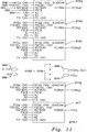
- the redundancy enable circuit (DISY) 316 receives as its inputs a power down signal (APDB) on line 384, the test signal PRETEST on line 386, the signal PREB0 ⁇ on line 388, the signal PREB1 on line 390, the redundancy column select signals YCOM0(6:0) on line 392, the redundancy column select signals YCOM1(6:0) on line 394, the column enable signal YEC0 ⁇ on line 396, and the column enable signal YCE1 on line 398.
- APDB power down signal
- the redundant enable block 316 In response to these input signals, the redundant enable block 316 generates a first redundancy signal RED0 ⁇ on line 395 for enabling the redundant column 0 ⁇ in one of the corresponding redundancy blocks 2-8, a second redundancy signal RED1 on line 397 for enabling the redundant element 1 in the same corresponding one of the redundant block 2-8, and a disabling signal DISYB on line 399 for disabling the regular column or Y-decoder 318c for the memory array 10 when a redundant address has been selected.
- a schematic circuit diagram of the redundant enable circuit 316 is shown in Figure 14.
- the redundant enable circuit 316 includes a first redundant pre-decoder circuit 146a, a second redundant pre-decoder circuit 146b, and a disable circuit 148.
- the first pre-decoder circuit 146a is used to generate a first redundant pre-decoder signal RPDECB0 ⁇ on line 150, which is inverted by an inverter 152 to produce the first redundancy signal RED0 ⁇ .
- the second pre-decoder circuit 146b is used to generate a second redundant pre-decoder signal RPDECB1 on line 154, which is inverted by an inverter 156 to produce a second redundancy signal RED1.
- the pre-decoder circuit 146a is comprised of NAND logic gates 158-170 and OR logic gates 172, 174.
- the signals PREB0 ⁇ and PRETESTB will both be high.
- the pre-decoder signal RPDECBq will be low only when all of the redundant column select signals YCOMq(6:0) and the column enable signal YCEq are high.
- the redundancy signal RED0 ⁇ will be high so as to enable the redundant element 0 ⁇ in one of the redundant blocks associated with the sector-based redundancy column address.
- the disabling circuit 148 is used to generate the disable signal DISYB on the line 399.
- the disable circuit 148 When the power down signal APDB is low, the disable circuit 148 will be inactive and the disable signal will remain high.
- the disable signal DISYB is fed to the regular column decoder 318c for disabling the same.
- the redundant column decoder 318a receives at its inputs the signals VCX, the first redundancy signal RED0 ⁇ , and the signal HERB on the respective lines 381, 383, and 385.
- the only difference between the decoder 318a and the decoder 318b is that the decoder 318b receives the second redundancy signal RED1 rather than the first redundancy signal.
- the decoder circuit 318a In response to these input signals, the decoder circuit 318a generates a redundant column signal RYD0 ⁇ on line 387, which is used to enable the appropriate redundancy block.
- a schematic circuit diagram of the decoder circuit 318a is shown in Figure 16 of the drawings.
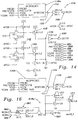
- a write protect fuse circuit 418 includes eight (8) identical minifuse circuits (MINICAMW) 420a-420h whose outputs are tied together so as to define an octfuse arrangement. It should be understood that each minifuse write protect circuit 420a-420h is associated with one of the 8 sectors.
- the sector addresses are decoded to generate the select signals SEL0 ⁇ -SEL7 which are used to select a corresponding one of the minifuse protect circuits 420a-420h to output its stored information onto the line WPC.
- the signal on the line WPC is passed through the pass transistor 422 and inverters 424-428 to the line 430.
- the write protect signal WPSB on the line 430 is used to disable write control circuitry (not shown) in the memory array.
- FIG. 18 A schematic circuit diagram of the minifuse write protect circuit 420a is depicted in Figure 18. It will be noted that the minifuse write protect circuit 420a is substantially identical in its construction to the minifuse circuit 319a ( Figure 13), except the common source of the poly devices in the minifuse write protect circuit is connected to receive an erase signal CAMERSH, which is tied to supply potential VPPE during the erase mode. In this manner, the minifuse write protect circuit which is formed of the write protect fuse cell can be erased.
- the overall operation of the addressable CAM peripheral architecture will be explained so as to enable the sector-based redundancy blocks 2-8 in Figure 1, which are used for repairing or replacing of a faulty (defective) column in a corresponding sector in a memory array 10.
- all of the sectors 12-26 in the memory array 10 are tested for defective memory cells in the corresponding columns and the column addresses for the defective memory cells are determined.
- the sector-based redundancy column addresses (corresponding to column addresses containing the defective columns of memory cells in the sector in association with one of the different redundant column segments to be used in repairing the defective column) are programmed and stored into the addressable fuse storage circuitry 314a and 314b via corresponding fuse select circuits 306a, 306b.
- each of the stored sector-based redundancy column addresses is associated with a redundant element in one of the sector-based redundancy blocks.
- the redundancy signals (RED0 ⁇ or RED1) from the redundant enable circuit 316 for enabling one of the redundant elements in the sector-based redundant block via the redundant Y-decoder 318a or 318b.
- the disable signal DISYB from the circuit 316 will also be generated so as to disable the regular Y-decoder 318c.
- the redundancy column address A15, A5-A0 will be stored in the quad address fuse circuits 315g-315a ( Figure 11). Within each of the quad address fuse circuits, the minifuse circuit 319d will be used for storing the corresponding bit address since it is the one associated with the redundancy block 8.
- the number of storage circuitry (ADDCAMX7) required is dependent upon the number of redundant elements in the redundancy blocks, one storage circuitry being needed for each redundant element.
- the number of quad address fuse circuits required within the storage circuitry is dependent upon the number of columns in the sector. One additional quad address fuse circuit is required for each time the number of columns in the sector is doubled.
- the number of minifuse circuits which are arrayed so as to share a common read line is dependent upon the number of redundancy blocks.
- the present invention provides an improved redundancy architecture for an array of flash EEPROM cells which permit replacing of defective columns in memory cells of the array with redundant columns of memory cells on a sector-by-sector basis.
- the redundant circuitry includes a plurality of sector-based redundancy blocks, each having redundant columns of memory cells and sector selection means for dividing a redundant column into different segments residing in corresponding ones of the sectors so as to allow for independent use from other segments in the same redundant columns.
- the redundant circuitry includes addressable fuse storage circuitry for storing sector-based redundancy column addresses.
Landscapes
- For Increasing The Reliability Of Semiconductor Memories (AREA)
- Read Only Memory (AREA)
- Semiconductor Memories (AREA)
Applications Claiming Priority (2)
| Application Number | Priority Date | Filing Date | Title |
|---|---|---|---|
| US112033 | 1993-08-26 | ||
| US08/112,033 US5349558A (en) | 1993-08-26 | 1993-08-26 | Sector-based redundancy architecture |
Publications (2)
| Publication Number | Publication Date |
|---|---|
| EP0640918A1 true EP0640918A1 (fr) | 1995-03-01 |
| EP0640918B1 EP0640918B1 (fr) | 1997-10-08 |
Family
ID=22341773
Family Applications (1)
| Application Number | Title | Priority Date | Filing Date |
|---|---|---|---|
| EP94305470A Expired - Lifetime EP0640918B1 (fr) | 1993-08-26 | 1994-07-25 | Circuit de mémoire intégré à semi-conducteur |
Country Status (5)
| Country | Link |
|---|---|
| US (1) | US5349558A (fr) |
| EP (1) | EP0640918B1 (fr) |
| JP (1) | JP3657290B2 (fr) |
| KR (1) | KR950006873A (fr) |
| DE (1) | DE69406074T2 (fr) |
Cited By (1)
| Publication number | Priority date | Publication date | Assignee | Title |
|---|---|---|---|---|
| EP0797145A1 (fr) * | 1996-03-22 | 1997-09-24 | STMicroelectronics S.r.l. | Dispositif de mémoire non volatile à effacement et programmation électriquement en secteur et avec redondance |
Families Citing this family (46)
| Publication number | Priority date | Publication date | Assignee | Title |
|---|---|---|---|---|
| US5359570A (en) * | 1992-11-13 | 1994-10-25 | Silicon Storage Technology, Inc. | Solid state peripheral storage device |
| JPH07230686A (ja) * | 1994-02-18 | 1995-08-29 | Toshiba Corp | 半導体記憶装置 |
| US5488701A (en) * | 1994-11-17 | 1996-01-30 | International Business Machines Corporation | In log sparing for log structured arrays |
| JPH08213572A (ja) * | 1994-11-30 | 1996-08-20 | Nkk Corp | 不揮発性半導体装置およびその製造方法 |
| DE69626792T2 (de) * | 1996-05-09 | 2004-03-25 | Stmicroelectronics S.R.L., Agrate Brianza | Elektrische löschbare und programmierbare nichtflüchtige Speicheranordnung mit prüfbaren Redundanzschaltungen |
| US5828599A (en) * | 1996-08-06 | 1998-10-27 | Simtek Corporation | Memory with electrically erasable and programmable redundancy |
| US6031757A (en) * | 1996-11-22 | 2000-02-29 | Macronix International Co., Ltd. | Write protected, non-volatile memory device with user programmable sector lock capability |
| WO1998022950A1 (fr) * | 1996-11-22 | 1998-05-28 | Macronix International Co., Ltd. | Memoire non volatile protegee en ecriture avec possibilite de verrouillage de secteur programmable par l'utilisateur |
| DE19880311B3 (de) * | 1997-02-12 | 2017-06-22 | Hyundai Electronics America Inc. | Nichtflüchtige Speicherstruktur |
| US5917763A (en) * | 1997-09-12 | 1999-06-29 | Micron Technology, Inc. | Method and apparatus for repairing opens on global column lines |
| DE59809488D1 (de) * | 1998-05-25 | 2003-10-09 | Abb Turbo Systems Ag Baden | Radialverdichter |
| US6260156B1 (en) | 1998-12-04 | 2001-07-10 | Datalight, Inc. | Method and system for managing bad areas in flash memory |
| JP2000231795A (ja) * | 1999-02-08 | 2000-08-22 | Sanyo Electric Co Ltd | 半導体メモリ装置 |
| US6397313B1 (en) * | 1999-10-19 | 2002-05-28 | Advanced Micro Devices, Inc. | Redundant dual bank architecture for a simultaneous operation flash memory |
| JP3893005B2 (ja) * | 2000-01-06 | 2007-03-14 | 富士通株式会社 | 不揮発性半導体記憶装置 |
| US6266281B1 (en) | 2000-02-16 | 2001-07-24 | Advanced Micro Devices, Inc. | Method of erasing non-volatile memory cells |
| US6285583B1 (en) * | 2000-02-17 | 2001-09-04 | Advanced Micro Devices, Inc. | High speed sensing to detect write protect state in a flash memory device |
| US6310805B1 (en) | 2000-03-07 | 2001-10-30 | Advanced Micro Devices, Inc. | Architecture for a dual-bank page mode memory with redundancy |
| JP2002063797A (ja) | 2000-08-22 | 2002-02-28 | Mitsubishi Electric Corp | 不揮発性半導体記憶装置 |
| US6813735B1 (en) | 2000-10-02 | 2004-11-02 | Fasl, Llc. | I/O based column redundancy for virtual ground with 2-bit cell flash memory |
| US6714467B2 (en) * | 2002-03-19 | 2004-03-30 | Broadcom Corporation | Block redundancy implementation in heirarchical RAM's |
| JP2003045195A (ja) * | 2001-07-31 | 2003-02-14 | Mitsubishi Electric Corp | 半導体メモリ |
| US6618316B2 (en) * | 2001-12-20 | 2003-09-09 | Intel Corporation | Pseudo-static single-ended cache cell |
| EP1468423A2 (fr) * | 2002-01-18 | 2004-10-20 | California Institute Of Technology | Architecture en reseau pour dispositifs electroniques moleculaires |
| KR100504114B1 (ko) * | 2002-08-23 | 2005-07-27 | 삼성전자주식회사 | 불량 셀 구제 기능을 갖는 롬 메모리 장치 및 불량 셀구제 방법 |
| WO2004109706A2 (fr) * | 2003-06-02 | 2004-12-16 | California Institute Of Technology | Reseaux logiques programmables sublithographiques a fils nanometriques |
| US7242601B2 (en) * | 2003-06-02 | 2007-07-10 | California Institute Of Technology | Deterministic addressing of nanoscale devices assembled at sublithographic pitches |
| US7509543B2 (en) * | 2003-06-17 | 2009-03-24 | Micron Technology, Inc. | Circuit and method for error test, recordation, and repair |
| US7437632B2 (en) * | 2003-06-24 | 2008-10-14 | Micron Technology, Inc. | Circuits and methods for repairing defects in memory devices |
| WO2005029498A2 (fr) * | 2003-07-24 | 2005-03-31 | California Institute Of Technology | Codage de fils a echelle nanometrique pour ensemble stochastique |
| KR100633595B1 (ko) * | 2004-04-20 | 2006-10-12 | 주식회사 하이닉스반도체 | 반도체 메모리 장치 및 그 구동 방법 |
| US7310004B2 (en) * | 2004-05-28 | 2007-12-18 | California Institute Of Technology | Apparatus and method of interconnecting nanoscale programmable logic array clusters |
| US6944075B1 (en) | 2005-01-05 | 2005-09-13 | International Business Machines Corporation | Variable column redundancy region boundaries in SRAM |
| US8072834B2 (en) | 2005-08-25 | 2011-12-06 | Cypress Semiconductor Corporation | Line driver circuit and method with standby mode of operation |
| US7636259B1 (en) | 2006-07-17 | 2009-12-22 | Lallice Semiconductor Corporation | Flash memory array with independently erasable sectors |
| US7512015B1 (en) | 2006-07-17 | 2009-03-31 | Lattice Semiconductor Corporation | Negative voltage blocking for embedded memories |
| KR100781976B1 (ko) | 2006-11-02 | 2007-12-06 | 삼성전자주식회사 | 플래시 메모리를 구비하는 반도체 메모리 장치에서의 블록상태 정보 제공방법 |
| JP2011518370A (ja) * | 2008-03-27 | 2011-06-23 | ジーイー・ヘルスケア・バイオサイエンス・バイオプロセス・コーポレイション | 使い捨てバイオプロセス部品の不正使用を防止する方法 |
| US8963684B2 (en) * | 2008-03-27 | 2015-02-24 | Ge Healthcare Bio-Sciences Corp | Gamma sterilizable RFID system that prevents unauthorized operation of associated disposable bioprocess components |
| US8327066B2 (en) | 2008-09-30 | 2012-12-04 | Samsung Electronics Co., Ltd. | Method of managing a solid state drive, associated systems and implementations |
| US8793558B2 (en) | 2012-08-27 | 2014-07-29 | Freescale Semiconductor, Inc. | Adaptive error correction for non-volatile memories |
| CN103544995B (zh) * | 2013-08-27 | 2016-09-21 | 华为技术有限公司 | 一种坏道修复方法及装置 |
| CN106548809A (zh) | 2015-09-22 | 2017-03-29 | 飞思卡尔半导体公司 | 处理缺陷非易失性存储器 |
| US10032515B2 (en) | 2016-02-26 | 2018-07-24 | Nxp Usa, Inc. | Memory repair system and method therefor |
| CN108735268B (zh) | 2017-04-19 | 2024-01-30 | 恩智浦美国有限公司 | 非易失性存储器修复电路 |
| KR102384864B1 (ko) | 2017-11-03 | 2022-04-08 | 삼성전자주식회사 | 불량 스트링을 리페어하는 방법 및 불휘발성 메모리 장치 |
Citations (2)
| Publication number | Priority date | Publication date | Assignee | Title |
|---|---|---|---|---|
| EP0448980A2 (fr) * | 1990-03-29 | 1991-10-02 | Texas Instruments Incorporated | Dispositif et procédé de réparation d'erreurs d'une mémoire |
| EP0549193A2 (fr) * | 1991-12-27 | 1993-06-30 | Nec Corporation | Dispositif de mémoire rémanente à semi-conducteur à redondance |
Family Cites Families (3)
| Publication number | Priority date | Publication date | Assignee | Title |
|---|---|---|---|---|
| US5088066A (en) * | 1989-02-10 | 1992-02-11 | Intel Corporation | Redundancy decoding circuit using n-channel transistors |
| US5270975A (en) * | 1990-03-29 | 1993-12-14 | Texas Instruments Incorporated | Memory device having a non-uniform redundancy decoder arrangement |
| US5278793A (en) * | 1992-02-25 | 1994-01-11 | Yeh Tsuei Chi | Memory defect masking device |
-
1993
- 1993-08-26 US US08/112,033 patent/US5349558A/en not_active Expired - Lifetime
-
1994
- 1994-07-25 EP EP94305470A patent/EP0640918B1/fr not_active Expired - Lifetime
- 1994-07-25 DE DE69406074T patent/DE69406074T2/de not_active Expired - Fee Related
- 1994-08-22 KR KR1019940020702A patent/KR950006873A/ko not_active Withdrawn
- 1994-08-24 JP JP19931594A patent/JP3657290B2/ja not_active Expired - Lifetime
Patent Citations (2)
| Publication number | Priority date | Publication date | Assignee | Title |
|---|---|---|---|---|
| EP0448980A2 (fr) * | 1990-03-29 | 1991-10-02 | Texas Instruments Incorporated | Dispositif et procédé de réparation d'erreurs d'une mémoire |
| EP0549193A2 (fr) * | 1991-12-27 | 1993-06-30 | Nec Corporation | Dispositif de mémoire rémanente à semi-conducteur à redondance |
Cited By (2)
| Publication number | Priority date | Publication date | Assignee | Title |
|---|---|---|---|---|
| EP0797145A1 (fr) * | 1996-03-22 | 1997-09-24 | STMicroelectronics S.r.l. | Dispositif de mémoire non volatile à effacement et programmation électriquement en secteur et avec redondance |
| US5854764A (en) * | 1996-03-22 | 1998-12-29 | Sgs-Thomson Microelectronics, S.R.L. | Sectorized electrically erasable and programmable non-volatile memory device with redundancy |
Also Published As
| Publication number | Publication date |
|---|---|
| EP0640918B1 (fr) | 1997-10-08 |
| US5349558A (en) | 1994-09-20 |
| DE69406074D1 (de) | 1997-11-13 |
| DE69406074T2 (de) | 1998-04-09 |
| JPH0798997A (ja) | 1995-04-11 |
| JP3657290B2 (ja) | 2005-06-08 |
| KR950006873A (ko) | 1995-03-21 |
Similar Documents
| Publication | Publication Date | Title |
|---|---|---|
| EP0640918B1 (fr) | Circuit de mémoire intégré à semi-conducteur | |
| US5200922A (en) | Redundancy circuit for high speed EPROM and flash memory devices | |
| US5973978A (en) | Anti-fuse programming path | |
| KR100205006B1 (ko) | 자동 결함 블럭 맵핑 기능을 갖는 반도체 메모리 장치 | |
| US5268866A (en) | Memory with column redundancy and localized column redundancy control signals | |
| JP4294971B2 (ja) | 不揮発性メモリ装置 | |
| US5606527A (en) | Methods for detecting short-circuited signal lines in nonvolatile semiconductor memory and circuitry therefor | |
| US4459685A (en) | Redundancy system for high speed, wide-word semiconductor memories | |
| KR950014802B1 (ko) | 불휘발성 반도체 메모리 장치 | |
| US6442084B2 (en) | Semiconductor memory having segmented row repair | |
| US5287310A (en) | Memory with I/O mappable redundant columns | |
| US6163489A (en) | Semiconductor memory having multiple redundant columns with offset segmentation boundaries | |
| JPH07153289A (ja) | 半導体集積回路メモリ装置 | |
| KR100200891B1 (ko) | 반도체 기억장치 | |
| US6418051B2 (en) | Non-volatile memory device with configurable row redundancy | |
| EP0503100B1 (fr) | Memoire a semi-conducteur | |
| US5808945A (en) | Semiconductor memory having redundant memory array | |
| US6208570B1 (en) | Redundancy test method for a semiconductor memory | |
| JP2000260199A (ja) | 半導体記憶装置 | |
| JP2540028B2 (ja) | 集積プログラミング回路 | |
| US5787043A (en) | Semiconductor memory device having a redundancy capability | |
| US5058071A (en) | Semiconductor memory device having means for repairing the memory device with respect to possible defective memory portions | |
| US6307787B1 (en) | Burst read incorporating output based redundancy | |
| US6788597B2 (en) | Memory device having programmable column segmentation to increase flexibility in bit repair | |
| US20120307578A1 (en) | Semiconductor device having redundant select line to replace regular select line |
Legal Events
| Date | Code | Title | Description |
|---|---|---|---|
| PUAI | Public reference made under article 153(3) epc to a published international application that has entered the european phase |
Free format text: ORIGINAL CODE: 0009012 |
|
| AK | Designated contracting states |
Kind code of ref document: A1 Designated state(s): BE DE DK ES FR GB GR IE IT LU NL PT SE |
|
| RIN1 | Information on inventor provided before grant (corrected) |
Inventor name: CLEVELAND, LEE E. Inventor name: VAN BUSKIRK, MICHAEL A. Inventor name: CHEN, JOHNNY C. Inventor name: CHANG, CHUNG K. |
|
| 17P | Request for examination filed |
Effective date: 19950608 |
|
| GRAG | Despatch of communication of intention to grant |
Free format text: ORIGINAL CODE: EPIDOS AGRA |
|
| 17Q | First examination report despatched |
Effective date: 19970128 |
|
| GRAH | Despatch of communication of intention to grant a patent |
Free format text: ORIGINAL CODE: EPIDOS IGRA |
|
| GRAH | Despatch of communication of intention to grant a patent |
Free format text: ORIGINAL CODE: EPIDOS IGRA |
|
| GRAA | (expected) grant |
Free format text: ORIGINAL CODE: 0009210 |
|
| AK | Designated contracting states |
Kind code of ref document: B1 Designated state(s): BE DE DK ES FR GB GR IE IT LU NL PT SE |
|
| PG25 | Lapsed in a contracting state [announced via postgrant information from national office to epo] |
Ref country code: NL Free format text: LAPSE BECAUSE OF FAILURE TO SUBMIT A TRANSLATION OF THE DESCRIPTION OR TO PAY THE FEE WITHIN THE PRESCRIBED TIME-LIMIT Effective date: 19971008 Ref country code: GR Free format text: LAPSE BECAUSE OF FAILURE TO SUBMIT A TRANSLATION OF THE DESCRIPTION OR TO PAY THE FEE WITHIN THE PRESCRIBED TIME-LIMIT Effective date: 19971008 Ref country code: ES Free format text: THE PATENT HAS BEEN ANNULLED BY A DECISION OF A NATIONAL AUTHORITY Effective date: 19971008 Ref country code: DK Free format text: LAPSE BECAUSE OF NON-PAYMENT OF DUE FEES Effective date: 19971008 Ref country code: BE Free format text: LAPSE BECAUSE OF FAILURE TO SUBMIT A TRANSLATION OF THE DESCRIPTION OR TO PAY THE FEE WITHIN THE PRESCRIBED TIME-LIMIT Effective date: 19971008 |
|
| ET | Fr: translation filed | ||
| REF | Corresponds to: |
Ref document number: 69406074 Country of ref document: DE Date of ref document: 19971113 |
|
| ITF | It: translation for a ep patent filed | ||
| PG25 | Lapsed in a contracting state [announced via postgrant information from national office to epo] |
Ref country code: SE Effective date: 19980108 Ref country code: PT Free format text: LAPSE BECAUSE OF FAILURE TO SUBMIT A TRANSLATION OF THE DESCRIPTION OR TO PAY THE FEE WITHIN THE PRESCRIBED TIME-LIMIT Effective date: 19980108 |
|
| NLV1 | Nl: lapsed or annulled due to failure to fulfill the requirements of art. 29p and 29m of the patents act | ||
| PG25 | Lapsed in a contracting state [announced via postgrant information from national office to epo] |
Ref country code: LU Free format text: LAPSE BECAUSE OF NON-PAYMENT OF DUE FEES Effective date: 19980725 Ref country code: IE Free format text: LAPSE BECAUSE OF NON-PAYMENT OF DUE FEES Effective date: 19980725 |
|
| PLBE | No opposition filed within time limit |
Free format text: ORIGINAL CODE: 0009261 |
|
| STAA | Information on the status of an ep patent application or granted ep patent |
Free format text: STATUS: NO OPPOSITION FILED WITHIN TIME LIMIT |
|
| 26N | No opposition filed | ||
| REG | Reference to a national code |
Ref country code: IE Ref legal event code: MM4A |
|
| REG | Reference to a national code |
Ref country code: GB Ref legal event code: IF02 |
|
| PGFP | Annual fee paid to national office [announced via postgrant information from national office to epo] |
Ref country code: GB Payment date: 20020613 Year of fee payment: 9 |
|
| PGFP | Annual fee paid to national office [announced via postgrant information from national office to epo] |
Ref country code: FR Payment date: 20020702 Year of fee payment: 9 |
|
| PGFP | Annual fee paid to national office [announced via postgrant information from national office to epo] |
Ref country code: DE Payment date: 20020731 Year of fee payment: 9 |
|
| PG25 | Lapsed in a contracting state [announced via postgrant information from national office to epo] |
Ref country code: GB Free format text: LAPSE BECAUSE OF NON-PAYMENT OF DUE FEES Effective date: 20030725 |
|
| PG25 | Lapsed in a contracting state [announced via postgrant information from national office to epo] |
Ref country code: DE Free format text: LAPSE BECAUSE OF NON-PAYMENT OF DUE FEES Effective date: 20040203 |
|
| GBPC | Gb: european patent ceased through non-payment of renewal fee |
Effective date: 20030725 |
|
| PG25 | Lapsed in a contracting state [announced via postgrant information from national office to epo] |
Ref country code: FR Free format text: LAPSE BECAUSE OF NON-PAYMENT OF DUE FEES Effective date: 20040331 |
|
| REG | Reference to a national code |
Ref country code: FR Ref legal event code: ST |
|
| PG25 | Lapsed in a contracting state [announced via postgrant information from national office to epo] |
Ref country code: IT Free format text: LAPSE BECAUSE OF NON-PAYMENT OF DUE FEES Effective date: 20050725 |