EP0641038A2 - Verfahren zum Verbinden eines biegsamen Substrates zu Kontaktobjekten und zu ihren Strukturen - Google Patents
Verfahren zum Verbinden eines biegsamen Substrates zu Kontaktobjekten und zu ihren Strukturen Download PDFInfo
- Publication number
- EP0641038A2 EP0641038A2 EP94113337A EP94113337A EP0641038A2 EP 0641038 A2 EP0641038 A2 EP 0641038A2 EP 94113337 A EP94113337 A EP 94113337A EP 94113337 A EP94113337 A EP 94113337A EP 0641038 A2 EP0641038 A2 EP 0641038A2
- Authority
- EP
- European Patent Office
- Prior art keywords
- contacted
- contact
- bump contacts
- portions
- laminate
- Prior art date
- Legal status (The legal status is an assumption and is not a legal conclusion. Google has not performed a legal analysis and makes no representation as to the accuracy of the status listed.)
- Granted
Links
Images



Classifications
-
- H—ELECTRICITY
- H01—ELECTRIC ELEMENTS
- H01R—ELECTRICALLY-CONDUCTIVE CONNECTIONS; STRUCTURAL ASSOCIATIONS OF A PLURALITY OF MUTUALLY-INSULATED ELECTRICAL CONNECTING ELEMENTS; COUPLING DEVICES; CURRENT COLLECTORS
- H01R13/00—Details of coupling devices of the kinds covered by groups H01R12/70 or H01R24/00 - H01R33/00
- H01R13/02—Contact members
- H01R13/22—Contacts for co-operating by abutting
- H01R13/24—Contacts for co-operating by abutting resilient; resiliently-mounted
- H01R13/2407—Contacts for co-operating by abutting resilient; resiliently-mounted characterized by the resilient means
- H01R13/2414—Contacts for co-operating by abutting resilient; resiliently-mounted characterized by the resilient means conductive elastomers
-
- H—ELECTRICITY
- H01—ELECTRIC ELEMENTS
- H01R—ELECTRICALLY-CONDUCTIVE CONNECTIONS; STRUCTURAL ASSOCIATIONS OF A PLURALITY OF MUTUALLY-INSULATED ELECTRICAL CONNECTING ELEMENTS; COUPLING DEVICES; CURRENT COLLECTORS
- H01R12/00—Structural associations of a plurality of mutually-insulated electrical connecting elements, specially adapted for printed circuits, e.g. printed circuit boards [PCB], flat or ribbon cables, or like generally planar structures, e.g. terminal strips, terminal blocks; Coupling devices specially adapted for printed circuits, flat or ribbon cables, or like generally planar structures; Terminals specially adapted for contact with, or insertion into, printed circuits, flat or ribbon cables, or like generally planar structures
- H01R12/50—Fixed connections
- H01R12/59—Fixed connections for flexible printed circuits, flat or ribbon cables or like structures
- H01R12/62—Fixed connections for flexible printed circuits, flat or ribbon cables or like structures connecting to rigid printed circuits or like structures
-
- H—ELECTRICITY
- H01—ELECTRIC ELEMENTS
- H01R—ELECTRICALLY-CONDUCTIVE CONNECTIONS; STRUCTURAL ASSOCIATIONS OF A PLURALITY OF MUTUALLY-INSULATED ELECTRICAL CONNECTING ELEMENTS; COUPLING DEVICES; CURRENT COLLECTORS
- H01R13/00—Details of coupling devices of the kinds covered by groups H01R12/70 or H01R24/00 - H01R33/00
- H01R13/02—Contact members
- H01R13/22—Contacts for co-operating by abutting
- H01R13/24—Contacts for co-operating by abutting resilient; resiliently-mounted
- H01R13/2464—Contacts for co-operating by abutting resilient; resiliently-mounted characterized by the contact point
-
- H—ELECTRICITY
- H05—ELECTRIC TECHNIQUES NOT OTHERWISE PROVIDED FOR
- H05K—PRINTED CIRCUITS; CASINGS OR CONSTRUCTIONAL DETAILS OF ELECTRIC APPARATUS; MANUFACTURE OF ASSEMBLAGES OF ELECTRICAL COMPONENTS
- H05K3/00—Apparatus or processes for manufacturing printed circuits
- H05K3/36—Assembling printed circuits with other printed circuits
- H05K3/361—Assembling flexible printed circuits with other printed circuits
- H05K3/365—Assembling flexible printed circuits with other printed circuits by abutting, i.e. without alloying process
-
- H—ELECTRICITY
- H10—SEMICONDUCTOR DEVICES; ELECTRIC SOLID-STATE DEVICES NOT OTHERWISE PROVIDED FOR
- H10W—GENERIC PACKAGES, INTERCONNECTIONS, CONNECTORS OR OTHER CONSTRUCTIONAL DETAILS OF DEVICES COVERED BY CLASS H10
- H10W72/00—Interconnections or connectors in packages
- H10W72/071—Connecting or disconnecting
- H10W72/072—Connecting or disconnecting of bump connectors
-
- H—ELECTRICITY
- H01—ELECTRIC ELEMENTS
- H01R—ELECTRICALLY-CONDUCTIVE CONNECTIONS; STRUCTURAL ASSOCIATIONS OF A PLURALITY OF MUTUALLY-INSULATED ELECTRICAL CONNECTING ELEMENTS; COUPLING DEVICES; CURRENT COLLECTORS
- H01R4/00—Electrically-conductive connections between two or more conductive members in direct contact, i.e. touching one another; Means for effecting or maintaining such contact; Electrically-conductive connections having two or more spaced connecting locations for conductors and using contact members penetrating insulation
- H01R4/04—Electrically-conductive connections between two or more conductive members in direct contact, i.e. touching one another; Means for effecting or maintaining such contact; Electrically-conductive connections having two or more spaced connecting locations for conductors and using contact members penetrating insulation using electrically conductive adhesives
-
- H—ELECTRICITY
- H10—SEMICONDUCTOR DEVICES; ELECTRIC SOLID-STATE DEVICES NOT OTHERWISE PROVIDED FOR
- H10W—GENERIC PACKAGES, INTERCONNECTIONS, CONNECTORS OR OTHER CONSTRUCTIONAL DETAILS OF DEVICES COVERED BY CLASS H10
- H10W72/00—Interconnections or connectors in packages
- H10W72/071—Connecting or disconnecting
- H10W72/072—Connecting or disconnecting of bump connectors
- H10W72/07231—Techniques
- H10W72/07236—Soldering or alloying
-
- Y—GENERAL TAGGING OF NEW TECHNOLOGICAL DEVELOPMENTS; GENERAL TAGGING OF CROSS-SECTIONAL TECHNOLOGIES SPANNING OVER SEVERAL SECTIONS OF THE IPC; TECHNICAL SUBJECTS COVERED BY FORMER USPC CROSS-REFERENCE ART COLLECTIONS [XRACs] AND DIGESTS
- Y10—TECHNICAL SUBJECTS COVERED BY FORMER USPC
- Y10T—TECHNICAL SUBJECTS COVERED BY FORMER US CLASSIFICATION
- Y10T29/00—Metal working
- Y10T29/49—Method of mechanical manufacture
- Y10T29/49002—Electrical device making
- Y10T29/49117—Conductor or circuit manufacturing
- Y10T29/49124—On flat or curved insulated base, e.g., printed circuit, etc.
- Y10T29/49155—Manufacturing circuit on or in base
Definitions
- the present invention relates to a suitable method for connecting a flexible circuit substrate to a contact object having a plurality of portions to be contacted, such as electronic parts and electronic circuits, and a structure thereof.
- the electronic parts are usually checked with respect to their characteristics and qualities at every stage of their manufacturing process. For example, at a stage at which a number of LSIs are formed on a silicon wafer or at a stage at which they are parted (the substances at these stages are hereinafter referred to as "bare chips"), a probe is required which can make contact with minute inspection objects densely arranged in an about 4 to 15 mm square region, simultaneously at multiple points with high reliability.
- a connecting structure using a flexible circuit substrate having projecting bump contacts on a surface thereof is known as a structure which can effect temporary contact or lasting connection to the above-described contact objects formed minutely and densely.
- Fig. 6 is a partial sectional schematic view showing a conventional flexible circuit substrate and a connected state thereof to a contact object.
- a1 is a conventional flexible circuit substrate in which a plurality of bump contacts 2 mounted on one surface of an electrically insulating film 1 are electrically connected to circuit patterns 3 provided on either surface of the film 1 or on an under layer of an electrically insulating protective film 4.
- the flexible circuit substrate a1 is laminated with a contact object b such that a plurality of portions 5 to be contacted on the contact object b such as an electric part are contacted with the above-described bump contacts 2, correspondingly each other.
- Pressure F is applied to the entire surfaces of the laminate in a compressing direction from the respective opposite surfaces of pressurizing means 6a and 6b which are provided such that the laminate is pinched therebetween in a laminating direction .
- the portions 5 to be contacted are contacted with the bump contacts 2, correspondingly each other.
- the height of the bump contacts themselves fluctuates by manufacturing errors, and in addition to this, the uniformities in the thickness of the electrically insulating film 1, the height of the portions 5 to be contacted on the contact object b, the flatness of a pressurizing surface of the pressurising means 6a, and the parallelism between the pressurizing means 6a and 6b are all accumulated in the laminating direction. It is therefore very difficult to uniformly contact all the bump contacts 2 with the corresponding portions 5 to be contacted. In particular, as shown in a portion enclosed with an alternate long and short dash line X in Fig. 6, a failure to contact the bump contact 2 with the portion 5 to be contacted causes such a connecting structure to lose contact reliability, which raises a serious problem.
- an object of the present invention is to provide a contacting method which enables all bump contacts on a flexible circuit substrate to contact with portions to be contacted on a contact object, the portions being formed minutely and densely.
- Another object of the present invention is to provide a connecting structure having higher contact reliability.
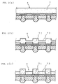
- the present invention provides a connecting method comprising laminating a flexible circuit substrate a having a plurality of bump contacts 2 with a contact object b having a plurality of portions 5 to be contacted such that the respective bump contacts face to the portions to be contacted at a joined surface, correspondingly each other to form a laminate, as shown in Fig. 1(a), and applying pressure F to the entire surface of the laminate in a compressing direction with pressurizing means 6a and 6b which are provided so as to pinch the laminate in a laminating direction to contact the plural bump contacts 2 mounted on the flexible circuit substrate a with the plural portions 5 to be contacted corresponding thereto mounted on the contact object b , respectively, as shown in Fig. 1(b).
- the pressure applied to the laminate is uniformly distributed among respective combinations of the bump contacts and the corresponding portions to be contacted.
- uniform distribution of the applied pressure can be relatively easily obtained by high-precision processing at levels of equipment such as inspection apparatus, but it is difficult to obtain such uniform distribution in case of minute contact objects or at levels of simple small-sized products such as card-like electric equipment.
- suitable pressurizing means which can apply uniform pressure even if connection is conducted at any manufacturing levels. That is, as shown in Fig. 3, at least either of the pressurizing means 6a and 6b collectively receives once pressure F applied from a pressurizing source 12 at a pressure carrier portion 10, and the pressure is dispersedly transmitted to the respective contacting portions of the bump contacts 2 and the portions 5 to be contacted through a transmitting portion 11.
- the applied pressure can be diffused over all the contact combinations with this pressurizing means, resulting in a more desirable connecting method.
- An elastic material may be mounted not only on the back side of the bump contact (designated by 7 in Fig. 1), but also at least on a position corresponding to the back side of the portion 5 to be contacted of the contact object b to intervene the elastic material between the portion 5 to be contacted and the pressurizing means 6b as designated by 7b in Fig. 1, thereby exerting an action similar to that exhibited by the elastic material 7 also on the portion to be contacted.
- 7b in Fig. 1 An elastic material may be mounted not only on the back side of the bump contact (designated by 7 in Fig. 1), but also at least on a position corresponding to the back side of the portion 5 to be contacted of the contact object b to intervene the elastic material between the portion 5 to be contacted and the pressurizing means 6b as designated by 7b in Fig. 1, thereby exerting an action similar to that exhibited by the elastic material 7 also on the portion to be contacted.
- more desirable contact can be obtained.
- the connecting method of the present invention exhibits the following function. That is, even if a combination which does not contact each other such as that of a bump contact 22 and a portion 52 to be contacted as denoted in a portion enclosed with an alternate long and short dash line Y in Fig. 1(a) is present in any position such as the margin or the central portion on the laminate, distribution of the uniform pressure to all the bumps strongly compresses the elastic materials 71 and 73 of contact combinations (for example, 21 and 51, and 23 and 53) around it as shown in Fig. 1(b) to absorb thickness errors accumulated in the laminating direction as described above. As a result, the combination which does not contact each other comes into contact, thus resulting in contacting all the bump contacts with the corresponding portions to be contacted.
- FIG. 1 is schematic sectional views showing a connecting structure of a flexible circuit substrate and a contact object according to one example of the present invention.
- A is a connecting structure of the present invention, which comprises a laminate prepared by laminating a flexible circuit substrate a with a contact object b such that a plurality of bump contacts 2 face to a plurality of portions 5 to be contacted at a jointed surface, correspondingly each other, and pressurizing means 6a and 6b which are provided so as to pinch the laminate in a laminating direction.
- pressure F is applied to the entire surface of the laminate from the pressurizing means 6a and 6b in a compressing direction to contact the bump contacts 2 with the portions 5 to be contacted, correspondingly each other.
- the flexible circuit substrate a may have any structure so long as the plural bump contacts 2 mounted on one surface of an insulating film 1 are electrically connected to circuit patterns 3 provided on either surface of the film 1 or in the inside thereof, and an elastic material 7 is mounted at least on a position corresponding to the back side of the bump contact.
- the bump contacts 2 on one surface of the electrically insulating film 1 are electrically connected to the circuit patterns 3 on the other surface in the inside of the film, or the bump contacts 2 and the circuit patterns 3 coexist on the same surface of the insulating film 1 and are electrically connected each other on the surface.
- the electrically insulating film 1 may be laminated in multiple.
- the electrically insulating film may have a structure such that the bump contacts are formed on the both sides of a first layer thereof and are electrically connected each other (so-called anisotropic electrically conductive film), which is laminated with an electrically insulating film having the circuit patterns.
- the shape of the bump contact is not always a projection, depending upon the shape of the corresponding portion to be contacted.
- the bump contact may be shaped into a flat form, and further may be depressed from a surface of the substrate.
- each is not structurally distinguished from a flexible circuit substrate in which a plurality of circuit patterns laminated in multiple electrically connect beyond between layers, but such a substrate also belongs to the above-described substrate a . That is, the flexible circuit substrate a used in the present invention may have any structure so long as its substrate has a flexibility and a function of electrical connection to the contact objects on the surface.
- the electrically insulating films 1 there is no particular restriction on the electrically insulating films 1 so long as it has an electrically insulating property and a flexibility.
- the film having an appropriate flexibility include polyester resins, epoxy resins, urethane resins, polystyrene resins, polyethylene resins, polyamide resins, polyimide resins, ABS resins, polycarbonate resins, silicone resins and fluororesins, irrespective of thermosetting or thermoplastic resins.
- Preferred examples of materials for the circuit patterns 3 include copper, nickel, solder, gold and silver.
- Methods for forming the circuit patterns 3 include a subtractive method and an additive method.
- the subtractive method is a method in which an insulating film is laminated with one to several electrically conductive layers through deposition or contact bonding, followed by etching to form circuit patterns.
- the additive method is a method in which circuit patterns are directly formed on an electrically insulating film through plating or deposition.
- the bump contacts 2 used in the present invention include gold, silver, copper, nickel, tin, solder and various alloys containing these as main components.
- the bump contacts 2 are formed not only by a single metal alone, but also as multi-layer structures comprising several kinds of metals according to the state of the portions to be contacted or the conditions of use. For example, when the bump contacts are used as contacts to which pressure is repeatedly applied, or when they are needed to penetrate into the portions to be contacted, it is preferred to form multi-layer structures in which comparatively hard metals such as nickel are used as core metals for the bump contacts, and good electrically conductive metals such as gold and solder are used as surface metals.
- Methods for forming the bump contacts 2 include a plating method such as an electrolytic plating or an electroless plating, a wire bonding method, and a cream solder potting method. Of these methods, the plating method such as electrolytic plating is preferred from the standpoints of easy formation of minute projecting contacts and good processability.
- the elastic materials 7 used in the present invention include those which utilize elastic deformation of materials themselves such as natural rubber, polymers and foamed products thereof, and those which have structures suitable for elastic displacement such as coiled springs. Those which utilize elastic deformation of materials themselves are particularly useful for minute connecting structures of highly close spacing.
- the materials showing the elastic deformation as described above preferably generate less deterioration in elasticity with the passage of time against repeated compression when they are used in process inspections, and against static load when they are lastingly incorporated into products, respectively.
- examples of such materials include elastomers and films of butadiene, nitrile, acrylic, ethylenepropylene, butyl, fluoro, silicone, styrene, urethane, ester, vinyl, olefin, amide, and imide, in addition to natural rubber. With technical progress, they may be replaced by novel elastic materials.
- the shape of the elastic materials 7 so long as they are mounted at least on positions corresponding to the back sides of the bump contacts of the substrate a . Examples thereof are shown in Fig. 1(a) and Figs. 2(a) to 2(C).
- Fig. 1(a) is an example in which the elastic materials 7 are formed separately and irrelevantly to one another in positions corresponding to the back sides of the respective bump contacts of the substrate.
- Examples of the individual shapes of the elastic materials 7 include pillars, cones, pyramids, frustums, spindles, complexes thereof and cylindrical bodies thereof each having a cross section vertical to the compressing direction such as a circle, an ellipse, a polygon and various modified shapes. For each of these, various parameters such as the cross-sectional area and the natural length can be selected.
- the embodiment shown in Fig. 2(a) is an example in which the elastic material 7 is formed in a plate form.
- the plate may be composed of a single material or may further be a laminate comprising a plurality of elastic materials.
- the laminate may partially contain a layer of a material showing elastic deformation. Further, the plate is freely provided with various penetration holes or concavities in predetermined positions thereof to give changes to the thickness of the layer.
- Fig. 2(b) is a sectional view showing an example in which the embodiments shown in Fig. 1(a) and Fig. 2(a) are combined.
- Elastic materials 71 formed individually in the positions corresponding to the back sides of the respective bump contacts of the substrate are constitutionally integrated with plate-like elastic materials 72.
- Such constitution offers both advantages of good independent compressibility of the elastic materials individually formed on the respective bump contacts, and low cost of the plate-like elastic materials and easy arrangement on the substrate.
- Fig. 2(c) is a sectional view showing an example in which plate-like portions 72 and projecting portions 71 are formed of different elastic materials. Such a combination makes it possible to distribute an arbitrary load in an arbitrary position.
- the projecting portions 71 may be minutely subdivided and each formed of different elastic materials, depending upon the purpose.
- the thickness of the plate-like portions 72 in the above-described embodiments may be freely set. For example, it can be set to the same thickness as that of the projecting portions 71.
- Methods for forming the elastic materials are largely divided into methods for directly forming the elastic materials on the substrates and methods for separately forming the elastic materials, and joining the same to the substrates.
- Useful examples of the methods for directly forming the elastic materials on the substrates include methods of applying precursor solutions or solutions of polymers to the substrates and drying them, methods of forming by the use of molds and various film forming methods, which may be subjected to shape processing by laser treatment or erosion. Further, protective films for the flexible circuit substrates can also be directly applied so long as materials on the back side surface of the bump contacts comprise elastic materials having a sufficient thickness.
- the elastic materials may be joined to the substrates either by permanent adhesive fixing using adhesives or melt adhesion, or by only overlapping of the elastic materials on the substrates.
- the pressurizing means 6a and 6b may be any means so long as they can uniformly apply the pressure F to all the respective connections of the bump contacts 2 and the portions 5 to be contacted.
- a structure having a pair of parallel flat surfaces facing each other is the easiest and most effective structure.
- the pressurizing means may have a structure having projections such that concentrated load can be applied to each of the connecting positions of the bump contacts 2 and the portions 5 to be contacted.
- the pressurizing sources may be transmitting media of compressing force obtained from power sources, such as high-pressure air and actuators.
- the compressing force may be maintained keeping the elastic materials in a deformed state by caulking or molding.
- Examples of the practical pressurizing means include a pressurizing structure comprising a stationary base and an inspection head which can be repeatedly opened and closed of an inspection instrument in inspection stages, etc., and when used in products, include various housings, cases and covers.
- FIG. 3 is schematic views showing structural examples of pressurizing means suitable for the connecting structures of the present invention.
- 6c is a structure on at least one side of the pressurizing means facing each other, which comprises a pressure carrier portion 10 collectively receiving pressure F from a pressurizing source 12 at one portion or predetermined plural portions, and a transmitting portion 11 for transmitting the pressure F collectively received by the pressure carrier portion 10 as pressure F uniformly dispersed to all the respective contacts of the bump contacts and the portions to be contacted.
- Fig. 3(a) shows an example in which a ball is used as the pressure carrier portion and received in a V-shaped groove, a conical recess or a spherical recess. This structure is excellent in uniform pressure distribution.
- Fig. 3(b) is a schematic view showing an example in which a projection 10 having an arbitrary shape such as a semi-spherical shape is integrated with a transmitting portion 11.
- Fig. 3(c) is a schematic view showing an example in which a projection 10 having an arbitrary shape is integrated with a pressurizing source 12.
- Fig. 3(d) is a schematic view showing an structural example in which a transmitting portion 11 has projections 11a which can distribute concentrated load to specified bump contacts. This can distribute the pressure to all the bump contacts with little loss.
- the structure as described above may be any structure, for example, a structure made up of a plurality of parts, so long as it collectively receives localized pressure at one point or a plurality of points if necessary, and uniformly distributes the concentrated pressure to the predetermined bump positions.
- the contact objects b may be any material of from minute objects to large-sized objects of product levels, such as LSIs of bare chip levels, TAB films to which the bare chips are connected, multichips obtained by integration thereof, various electronic parts, circuit substrates on which the electronic parts are mounted in large numbers and objects similar to the flexible circuit substrates a . Contacts and electrically conductive portions formed on these surfaces are used as the portions to be contacted for connection in the present invention.
- the connecting methods of the present invention are used in various states, for example, from brief contact as in probes or relay contacts to permanent fixing in contacted and pressed states as finished products or melt fixing after contact.
- a conventional flexible circuit substrate having bump contacts was provided with an elastic material, and the resulting product was laminated with a copper plate. Pressure was uniformly applied from the outside of the layer such that the bump contacts are contacted with the copper plate, and the contact state of the respective bump contacts with the copper plate was observed, thereby examining the contact reliability of the connecting structure of the present invention.
- Fig. 4 is a schematic view showing a constitution of this experiment.
- 400 nickel bump contacts 2 having a height of 15 ⁇ m were formed on a 25 ⁇ m thick polyimide insulating film 1 in total at 100 ⁇ m spacings so as to form four sides of a 10 mm square (so that 101 bump contacts per side form a line, sharing the bump contact at an apex of the square), and electrically connect to circuit patterns 3 on the back side, respectively.
- the elastic material 7 used was a 0.3 mm thick plate as shown in Fig. 2(a), the plate being formed of silicone rubber having a Shore hardness of A40, and joined to the substrate only by overlapping without fixing by adhesion.
- a pressurizing means 6c with which the pressure was uniformly dispersible as shown in Fig. 3(a) was mounted on the bump contact side of a compression tester which could arbitrarily set the pressure.
- the above-described conventional flexible circuit substrate a having the bump contacts was laminated with a copper plate b , and the elastic material and the pressurizing means were added thereto to constitute the connecting structure as shown in Fig. 4.
- the circuit patterns 3 electrically connecting to the respective bump contacts were connected to a measuring instrument D to make it possible to confirm the contact state of all the respective bump contacts with the copper plate.
- LSI pads in a bare chip state were corresponded to bump contacts on a flexible circuit substrate, and pressure was uniformly applied from the outside of the layer so as to contact with each other.
- the contact state of the respective bump contacts with the LSI pads was observed, thereby examining the usefulness of mounting of the connecting structure of the present invention.
- Fig. 5 is a schematic view showing a constitution of this experiment.
- the flexible circuit substrate a with the bump contacts having an elastic sheet 7 was mounted on a housing which is one pressurizing means 6a, and the LSI bare chip was used as a contact object b.
- the substrate a and the LSI bare chip b were overlapped each other such that the pads 5 corresponded to the bump contacts 2, and the back surface of the LSI bare chip was also overlapped with an elastic sheet 7b. Pressure was then applied by the other pressurizing means 6b.
- the present invention it becomes possible to contact all the bump contacts on the flexible circuit substrate with the portions to be contacted on the contact object, the portions being formed minutely and densely as LSIs of bare chip levels.
- the connecting structure having high contact reliability to process inspections of small-sized electronic instrument products and connected portions themselves in the products can be provided.
Landscapes
- Engineering & Computer Science (AREA)
- Metallurgy (AREA)
- Manufacturing & Machinery (AREA)
- Microelectronics & Electronic Packaging (AREA)
- Measuring Leads Or Probes (AREA)
- Wire Bonding (AREA)
- Coupling Device And Connection With Printed Circuit (AREA)
Applications Claiming Priority (3)
| Application Number | Priority Date | Filing Date | Title |
|---|---|---|---|
| JP5213146A JP2867209B2 (ja) | 1993-08-27 | 1993-08-27 | フレキシブル回路基板と接触対象物との接続方法およびその構造 |
| JP213146/93 | 1993-08-27 | ||
| JP21314693 | 1993-08-27 |
Publications (3)
| Publication Number | Publication Date |
|---|---|
| EP0641038A2 true EP0641038A2 (de) | 1995-03-01 |
| EP0641038A3 EP0641038A3 (de) | 1997-04-02 |
| EP0641038B1 EP0641038B1 (de) | 2001-11-07 |
Family
ID=16634344
Family Applications (1)
| Application Number | Title | Priority Date | Filing Date |
|---|---|---|---|
| EP94113337A Expired - Lifetime EP0641038B1 (de) | 1993-08-27 | 1994-08-25 | Verfahren zum Verbinden eines biegsamen Substrates zu Kontaktobjekten und zu ihren Strukturen |
Country Status (5)
| Country | Link |
|---|---|
| US (1) | US5575662A (de) |
| EP (1) | EP0641038B1 (de) |
| JP (1) | JP2867209B2 (de) |
| KR (1) | KR950005337A (de) |
| DE (1) | DE69428955T2 (de) |
Cited By (9)
| Publication number | Priority date | Publication date | Assignee | Title |
|---|---|---|---|---|
| WO1997003482A1 (en) * | 1995-07-07 | 1997-01-30 | Minnesotta Mining And Manufacturing Company | Separable electrical connector assembly having a planar array of conductive protrusions |
| EP0751565A3 (de) * | 1995-06-30 | 1998-09-30 | Nitto Denko Corporation | Filmträger für Halbleiter |
| DE19838418A1 (de) * | 1998-08-24 | 2000-03-02 | Delphi Automotive Systems Gmbh | Elektrische Anschlußvorrichtung sowie Verfahren zur Herstellung einer elektrischen Kontaktierung |
| US6100596A (en) * | 1996-03-19 | 2000-08-08 | Methode Electronics, Inc. | Connectorized substrate and method of connectorizing a substrate |
| EP1024554A3 (de) * | 1999-01-28 | 2000-10-04 | Intercon Systems, Inc. | Druckverbinderbaugruppe für flexible Schaltung und Herstellungsverfahren |
| EP1071032A3 (de) * | 1999-07-19 | 2002-09-04 | Nokia Corporation | Kartenleser |
| WO2003075408A1 (en) | 2002-03-07 | 2003-09-12 | Jsr Corporation | Anisotropic conductive connector and its production method, and circuit device test instrument |
| EP1870964A3 (de) * | 2006-06-23 | 2008-12-03 | Delphi Technologies, Inc. | Lötfreie elektrische Verbindung für ein Elektronikgehäuse |
| CN119714614A (zh) * | 2024-12-19 | 2025-03-28 | 德力西电气有限公司 | 继电器触头压力的调试方法、装置、设备和存储介质 |
Families Citing this family (42)
| Publication number | Priority date | Publication date | Assignee | Title |
|---|---|---|---|---|
| KR970707444A (ko) * | 1994-10-28 | 1997-12-01 | 야마모토 히데키 | 프로브 구조(probe structure) |
| US5776824A (en) | 1995-12-22 | 1998-07-07 | Micron Technology, Inc. | Method for producing laminated film/metal structures for known good die ("KG") applications |
| US5899757A (en) * | 1997-11-03 | 1999-05-04 | Intercon Systems, Inc. | Compression connector |
| US6156484A (en) * | 1997-11-07 | 2000-12-05 | International Business Machines Corporation | Gray scale etching for thin flexible interposer |
| CN1166265C (zh) | 1998-04-09 | 2004-09-08 | 精工爱普生株式会社 | 压接连接衬底、液晶装置及电子设备 |
| KR100485967B1 (ko) * | 1998-04-09 | 2005-05-03 | 세이코 엡슨 가부시키가이샤 | 압착 접속 기판, 액정 장치 및 전자 기기 |
| US6580035B1 (en) * | 1998-04-24 | 2003-06-17 | Amerasia International Technology, Inc. | Flexible adhesive membrane and electronic device employing same |
| JP2000106482A (ja) * | 1998-07-29 | 2000-04-11 | Sony Chem Corp | フレキシブル基板製造方法 |
| JP2001077501A (ja) * | 1999-09-03 | 2001-03-23 | Seiko Epson Corp | フレキシブル配線基板、電気光学装置および電子機器 |
| US6230400B1 (en) * | 1999-09-17 | 2001-05-15 | George Tzanavaras | Method for forming interconnects |
| JP3741927B2 (ja) * | 2000-03-31 | 2006-02-01 | 日本電気株式会社 | 半導体チップ又はパッケージ検査装置及びその検査方法 |
| DE10028184A1 (de) * | 2000-06-09 | 2002-03-07 | Hirschmann Austria Gmbh Rankwe | Vorrichtung zum Verbindung von elektrischen Leitern |
| KR100600092B1 (ko) * | 2000-06-28 | 2006-07-13 | 닛폰 하츠죠 가부시키가이샤 | 도전성 접촉자 |
| JP2002090388A (ja) * | 2000-09-13 | 2002-03-27 | Soushiyou Tec:Kk | リードの接点構造 |
| US6425768B1 (en) | 2000-11-17 | 2002-07-30 | Intercon Systems, Inc. | Clamp connector assembly |
| US6818545B2 (en) | 2001-03-05 | 2004-11-16 | Megic Corporation | Low fabrication cost, fine pitch and high reliability solder bump |
| US20030094666A1 (en) * | 2001-11-16 | 2003-05-22 | R-Tec Corporation | Interposer |
| US6881072B2 (en) * | 2002-10-01 | 2005-04-19 | International Business Machines Corporation | Membrane probe with anchored elements |
| US6839965B2 (en) * | 2003-02-06 | 2005-01-11 | R-Tec Corporation | Method of manufacturing a resistor connector |
| US20070020960A1 (en) | 2003-04-11 | 2007-01-25 | Williams John D | Contact grid array system |
| US7114961B2 (en) | 2003-04-11 | 2006-10-03 | Neoconix, Inc. | Electrical connector on a flexible carrier |
| US7758351B2 (en) | 2003-04-11 | 2010-07-20 | Neoconix, Inc. | Method and system for batch manufacturing of spring elements |
| US7597561B2 (en) | 2003-04-11 | 2009-10-06 | Neoconix, Inc. | Method and system for batch forming spring elements in three dimensions |
| US8584353B2 (en) | 2003-04-11 | 2013-11-19 | Neoconix, Inc. | Method for fabricating a contact grid array |
| US7244125B2 (en) | 2003-12-08 | 2007-07-17 | Neoconix, Inc. | Connector for making electrical contact at semiconductor scales |
| US7628617B2 (en) | 2003-06-11 | 2009-12-08 | Neoconix, Inc. | Structure and process for a contact grid array formed in a circuitized substrate |
| TWI239685B (en) * | 2003-05-13 | 2005-09-11 | Jsr Corp | Flaky probe, its manufacturing method and its application |
| US7383632B2 (en) | 2004-03-19 | 2008-06-10 | Neoconix, Inc. | Method for fabricating a connector |
| US7347698B2 (en) | 2004-03-19 | 2008-03-25 | Neoconix, Inc. | Deep drawn electrical contacts and method for making |
| US7354276B2 (en) | 2004-07-20 | 2008-04-08 | Neoconix, Inc. | Interposer with compliant pins |
| US6991473B1 (en) * | 2004-11-30 | 2006-01-31 | International Business Machines Corporation | Electrical connector with elastomeric pad having compressor fingers each including a filler member to mitigate relaxation of the elastomer |
| JP2007062036A (ja) * | 2005-08-29 | 2007-03-15 | Seiko Epson Corp | 液滴吐出ヘッド及び液滴吐出装置並びに液滴吐出ヘッドの製造方法 |
| US7357644B2 (en) | 2005-12-12 | 2008-04-15 | Neoconix, Inc. | Connector having staggered contact architecture for enhanced working range |
| JP4059522B1 (ja) * | 2006-10-27 | 2008-03-12 | 株式会社旭電化研究所 | 電気接続構造、それに用いる第1の接続部材 |
| US20090112767A1 (en) * | 2007-10-25 | 2009-04-30 | Ayman Hammad | Escrow system and method |
| US7841078B2 (en) * | 2008-01-07 | 2010-11-30 | International Business Machines Corporation | Method of optimizing land grid array geometry |
| JP2010098046A (ja) * | 2008-10-15 | 2010-04-30 | Renesas Technology Corp | プローブカードおよび半導体装置の製造方法 |
| CN102035085B (zh) * | 2009-10-08 | 2014-03-05 | 群康科技(深圳)有限公司 | 导电结构及其制造方法 |
| JP5798848B2 (ja) * | 2011-09-14 | 2015-10-21 | デクセリアルズ株式会社 | 接続方法及び接続構造体の製造方法 |
| US8641428B2 (en) | 2011-12-02 | 2014-02-04 | Neoconix, Inc. | Electrical connector and method of making it |
| US9680273B2 (en) | 2013-03-15 | 2017-06-13 | Neoconix, Inc | Electrical connector with electrical contacts protected by a layer of compressible material and method of making it |
| KR102341794B1 (ko) * | 2015-01-15 | 2021-12-21 | 삼성디스플레이 주식회사 | 가요성 표시 장치 및 그 제조 방법 |
Family Cites Families (9)
| Publication number | Priority date | Publication date | Assignee | Title |
|---|---|---|---|---|
| US4453795A (en) * | 1975-12-01 | 1984-06-12 | Hughes Aircraft Company | Cable-to-cable/component electrical pressure wafer connector assembly |
| US4184729A (en) * | 1977-10-13 | 1980-01-22 | Bunker Ramo Corporation | Flexible connector cable |
| US4647125A (en) * | 1985-07-22 | 1987-03-03 | Rogers Corporation | Solderless connector technique |
| US4813129A (en) * | 1987-06-19 | 1989-03-21 | Hewlett-Packard Company | Interconnect structure for PC boards and integrated circuits |
| EP0338717A3 (de) * | 1988-04-21 | 1990-10-17 | McMURDO LIMITED | Verbinderanordnung |
| NL8900676A (nl) * | 1989-03-20 | 1990-10-16 | Philips Nv | Substraat met interconnectiestructuren. |
| US5069628A (en) * | 1990-03-13 | 1991-12-03 | Hughes Aircraft Company | Flexible electrical cable connector with double sided dots |
| US5147208A (en) * | 1991-06-28 | 1992-09-15 | Rogers Corporation | Flexible printed circuit with raised contacts |
| JPH07105420B2 (ja) * | 1991-08-26 | 1995-11-13 | ヒューズ・エアクラフト・カンパニー | 成形された接点をもった電気接続 |
-
1993
- 1993-08-27 JP JP5213146A patent/JP2867209B2/ja not_active Expired - Fee Related
-
1994
- 1994-08-11 US US08/288,913 patent/US5575662A/en not_active Expired - Fee Related
- 1994-08-25 EP EP94113337A patent/EP0641038B1/de not_active Expired - Lifetime
- 1994-08-25 DE DE69428955T patent/DE69428955T2/de not_active Expired - Fee Related
- 1994-08-26 KR KR1019940021136A patent/KR950005337A/ko not_active Withdrawn
Cited By (14)
| Publication number | Priority date | Publication date | Assignee | Title |
|---|---|---|---|---|
| KR100391022B1 (ko) * | 1995-06-30 | 2003-09-29 | 니토 덴코 가부시키가이샤 | 필름캐리어,필름캐리어를사용한반도체장치및반도체소자를장착하는방법 |
| EP0751565A3 (de) * | 1995-06-30 | 1998-09-30 | Nitto Denko Corporation | Filmträger für Halbleiter |
| US5876215A (en) * | 1995-07-07 | 1999-03-02 | Minnesota Mining And Manufacturing Company | Separable electrical connector assembly having a planar array of conductive protrusions |
| WO1997003482A1 (en) * | 1995-07-07 | 1997-01-30 | Minnesotta Mining And Manufacturing Company | Separable electrical connector assembly having a planar array of conductive protrusions |
| US6100596A (en) * | 1996-03-19 | 2000-08-08 | Methode Electronics, Inc. | Connectorized substrate and method of connectorizing a substrate |
| DE19838418A1 (de) * | 1998-08-24 | 2000-03-02 | Delphi Automotive Systems Gmbh | Elektrische Anschlußvorrichtung sowie Verfahren zur Herstellung einer elektrischen Kontaktierung |
| SG90059A1 (en) * | 1999-01-28 | 2002-07-23 | Intercon Systems Inc | Flexible circuit compression connector system and method of manufacture |
| EP1024554A3 (de) * | 1999-01-28 | 2000-10-04 | Intercon Systems, Inc. | Druckverbinderbaugruppe für flexible Schaltung und Herstellungsverfahren |
| EP1071032A3 (de) * | 1999-07-19 | 2002-09-04 | Nokia Corporation | Kartenleser |
| WO2003075408A1 (en) | 2002-03-07 | 2003-09-12 | Jsr Corporation | Anisotropic conductive connector and its production method, and circuit device test instrument |
| EP1482593A4 (de) * | 2002-03-07 | 2010-11-03 | Jsr Corp | Anisotroper leitfähiger verbinder und verfahren zu seiner herstellung und schaltungs einrichtungprüfinstrument |
| EP1870964A3 (de) * | 2006-06-23 | 2008-12-03 | Delphi Technologies, Inc. | Lötfreie elektrische Verbindung für ein Elektronikgehäuse |
| US7621757B2 (en) | 2006-06-23 | 2009-11-24 | Delphi Technologies, Inc. | Solderless electrical interconnection for electronic package |
| CN119714614A (zh) * | 2024-12-19 | 2025-03-28 | 德力西电气有限公司 | 继电器触头压力的调试方法、装置、设备和存储介质 |
Also Published As
| Publication number | Publication date |
|---|---|
| EP0641038B1 (de) | 2001-11-07 |
| JP2867209B2 (ja) | 1999-03-08 |
| US5575662A (en) | 1996-11-19 |
| JPH0766240A (ja) | 1995-03-10 |
| EP0641038A3 (de) | 1997-04-02 |
| KR950005337A (ko) | 1995-03-20 |
| DE69428955D1 (de) | 2001-12-13 |
| DE69428955T2 (de) | 2002-04-04 |
Similar Documents
| Publication | Publication Date | Title |
|---|---|---|
| US5575662A (en) | Methods for connecting flexible circuit substrates to contact objects and structures thereof | |
| US5759047A (en) | Flexible circuitized interposer with apertured member and method for making same | |
| US6705876B2 (en) | Electrical interconnect assemblies and methods | |
| US5857858A (en) | Demountable and repairable low pitch interconnect for stacked multichip modules | |
| US6524115B1 (en) | Compliant interconnect assembly | |
| US5829988A (en) | Socket assembly for integrated circuit chip carrier package | |
| EP1744167B1 (de) | Blattartige sonde, verfahren zur herstellung der sonde und anwendung der sonde | |
| US6358627B2 (en) | Rolling ball connector | |
| JP4871520B2 (ja) | 多重回路板間の高密度接続 | |
| JPH09312176A (ja) | 接続部材および該接続部材を用いた電極の接続構造並びに接続方法 | |
| KR100913686B1 (ko) | 이방성 전기 전도성 접착 필름, 이의 제조방법 및 이를 포함하는 반도체 장치 | |
| JP2002279830A (ja) | 異方導電性フィルム | |
| JPS60240074A (ja) | プリント回路ボ−ド用コネクタ | |
| JP2000221209A (ja) | 半導体素子の検査方法およびそのための異方導電性フィルム | |
| US5432679A (en) | Pressure equalizer for an integrated circuit chip interconnected to circuitry on a thin film membrane | |
| US5497103A (en) | Test apparatus for circuitized substrate | |
| KR100345899B1 (ko) | 전자 장치용 시험장치 | |
| JP2002124319A (ja) | 異方導電性フィルムおよびそれを用いた半導体素子または電子部品の検査方法 | |
| JP4041619B2 (ja) | インターコネクタの製造方法 | |
| KR101532390B1 (ko) | 절연성 시트, 절연성 시트의 제조방법 및 전기적 검사장치 | |
| JPH0574512A (ja) | 電気接続用コネクタ | |
| JPH0778645A (ja) | 電気接続用コネクタ | |
| JPH10125369A (ja) | 電子部品の接続方法及び接続構造 | |
| JP3033594B2 (ja) | 検査装置 | |
| JPH11329541A (ja) | 異方導電性コネクタ |
Legal Events
| Date | Code | Title | Description |
|---|---|---|---|
| PUAI | Public reference made under article 153(3) epc to a published international application that has entered the european phase |
Free format text: ORIGINAL CODE: 0009012 |
|
| AK | Designated contracting states |
Kind code of ref document: A2 Designated state(s): DE FR GB NL |
|
| PUAL | Search report despatched |
Free format text: ORIGINAL CODE: 0009013 |
|
| AK | Designated contracting states |
Kind code of ref document: A3 Designated state(s): DE FR GB NL |
|
| 17P | Request for examination filed |
Effective date: 19970528 |
|
| 17Q | First examination report despatched |
Effective date: 19990330 |
|
| GRAG | Despatch of communication of intention to grant |
Free format text: ORIGINAL CODE: EPIDOS AGRA |
|
| GRAG | Despatch of communication of intention to grant |
Free format text: ORIGINAL CODE: EPIDOS AGRA |
|
| GRAH | Despatch of communication of intention to grant a patent |
Free format text: ORIGINAL CODE: EPIDOS IGRA |
|
| GRAH | Despatch of communication of intention to grant a patent |
Free format text: ORIGINAL CODE: EPIDOS IGRA |
|
| RIC1 | Information provided on ipc code assigned before grant |
Free format text: 7H 01R 12/38 A, 7H 01R 13/24 B, 7H 01L 21/60 B |
|
| GRAA | (expected) grant |
Free format text: ORIGINAL CODE: 0009210 |
|
| AK | Designated contracting states |
Kind code of ref document: B1 Designated state(s): DE FR GB NL |
|
| REF | Corresponds to: |
Ref document number: 69428955 Country of ref document: DE Date of ref document: 20011213 |
|
| REG | Reference to a national code |
Ref country code: GB Ref legal event code: IF02 |
|
| ET | Fr: translation filed | ||
| PLBE | No opposition filed within time limit |
Free format text: ORIGINAL CODE: 0009261 |
|
| STAA | Information on the status of an ep patent application or granted ep patent |
Free format text: STATUS: NO OPPOSITION FILED WITHIN TIME LIMIT |
|
| 26N | No opposition filed | ||
| PGFP | Annual fee paid to national office [announced via postgrant information from national office to epo] |
Ref country code: FR Payment date: 20030808 Year of fee payment: 10 |
|
| PGFP | Annual fee paid to national office [announced via postgrant information from national office to epo] |
Ref country code: GB Payment date: 20030820 Year of fee payment: 10 |
|
| PGFP | Annual fee paid to national office [announced via postgrant information from national office to epo] |
Ref country code: NL Payment date: 20030831 Year of fee payment: 10 |
|
| PGFP | Annual fee paid to national office [announced via postgrant information from national office to epo] |
Ref country code: DE Payment date: 20030904 Year of fee payment: 10 |
|
| PG25 | Lapsed in a contracting state [announced via postgrant information from national office to epo] |
Ref country code: GB Free format text: LAPSE BECAUSE OF NON-PAYMENT OF DUE FEES Effective date: 20040825 |
|
| PG25 | Lapsed in a contracting state [announced via postgrant information from national office to epo] |
Ref country code: NL Free format text: LAPSE BECAUSE OF NON-PAYMENT OF DUE FEES Effective date: 20050301 Ref country code: DE Free format text: LAPSE BECAUSE OF NON-PAYMENT OF DUE FEES Effective date: 20050301 |
|
| GBPC | Gb: european patent ceased through non-payment of renewal fee |
Effective date: 20040825 |
|
| PG25 | Lapsed in a contracting state [announced via postgrant information from national office to epo] |
Ref country code: FR Free format text: LAPSE BECAUSE OF NON-PAYMENT OF DUE FEES Effective date: 20050429 |
|
| NLV4 | Nl: lapsed or anulled due to non-payment of the annual fee |
Effective date: 20050301 |
|
| REG | Reference to a national code |
Ref country code: FR Ref legal event code: ST |