EP0641091A1 - Vorrichtung mit entscheidungsgesteuerter Kanalschätzung in einer digitalen Mobilfunkverbindung - Google Patents
Vorrichtung mit entscheidungsgesteuerter Kanalschätzung in einer digitalen Mobilfunkverbindung Download PDFInfo
- Publication number
- EP0641091A1 EP0641091A1 EP94110653A EP94110653A EP0641091A1 EP 0641091 A1 EP0641091 A1 EP 0641091A1 EP 94110653 A EP94110653 A EP 94110653A EP 94110653 A EP94110653 A EP 94110653A EP 0641091 A1 EP0641091 A1 EP 0641091A1
- Authority
- EP
- European Patent Office
- Prior art keywords
- output
- signal
- multiplying
- adder
- input
- Prior art date
- Legal status (The legal status is an assumption and is not a legal conclusion. Google has not performed a legal analysis and makes no representation as to the accuracy of the status listed.)
- Granted
Links
Images




Classifications
-
- H—ELECTRICITY
- H04—ELECTRIC COMMUNICATION TECHNIQUE
- H04B—TRANSMISSION
- H04B1/00—Details of transmission systems, not covered by a single one of groups H04B3/00 - H04B13/00; Details of transmission systems not characterised by the medium used for transmission
- H04B1/69—Spread spectrum techniques
- H04B1/707—Spread spectrum techniques using direct sequence modulation
- H04B1/7097—Interference-related aspects
- H04B1/711—Interference-related aspects the interference being multi-path interference
- H04B1/7115—Constructive combining of multi-path signals, i.e. RAKE receivers
- H04B1/712—Weighting of fingers for combining, e.g. amplitude control or phase rotation using an inner loop
-
- H—ELECTRICITY
- H04—ELECTRIC COMMUNICATION TECHNIQUE
- H04B—TRANSMISSION
- H04B1/00—Details of transmission systems, not covered by a single one of groups H04B3/00 - H04B13/00; Details of transmission systems not characterised by the medium used for transmission
- H04B1/69—Spread spectrum techniques
- H04B1/707—Spread spectrum techniques using direct sequence modulation
-
- H—ELECTRICITY
- H04—ELECTRIC COMMUNICATION TECHNIQUE
- H04B—TRANSMISSION
- H04B1/00—Details of transmission systems, not covered by a single one of groups H04B3/00 - H04B13/00; Details of transmission systems not characterised by the medium used for transmission
- H04B1/69—Spread spectrum techniques
- H04B1/707—Spread spectrum techniques using direct sequence modulation
- H04B1/7097—Interference-related aspects
- H04B1/711—Interference-related aspects the interference being multi-path interference
- H04B1/7115—Constructive combining of multi-path signals, i.e. RAKE receivers
-
- H—ELECTRICITY
- H04—ELECTRIC COMMUNICATION TECHNIQUE
- H04B—TRANSMISSION
- H04B1/00—Details of transmission systems, not covered by a single one of groups H04B3/00 - H04B13/00; Details of transmission systems not characterised by the medium used for transmission
- H04B1/69—Spread spectrum techniques
- H04B1/707—Spread spectrum techniques using direct sequence modulation
- H04B1/7097—Interference-related aspects
- H04B1/711—Interference-related aspects the interference being multi-path interference
- H04B1/7115—Constructive combining of multi-path signals, i.e. RAKE receivers
- H04B1/7117—Selection, re-selection, allocation or re-allocation of paths to fingers, e.g. timing offset control of allocated fingers
Definitions
- the present invention relates to apparatus for use in equipment providing a digital radio link between a fixed and a mobile radio unit.
- FIG. 1 In which a plurality of Rake fingers are shown 10, 12, 14, 16. Each Rake finger comprises a signal correlator 18 which handles an inphase signal from a down-converter, and a further signal correlator 20 which handles a quadrature phase signal from a down-converter.
- the output signal from the correlator 18 is applied to a half linear multiplier 22 by way of a one bit delay circuit 26.
- the output of the half linear multiplier 22 is applied to an input of a Wiener-like filter 30.
- the output of the Wiener-like filter 30 is applied to a multiplier 34.
- the output of the correlator 18 is also applied to a further input of the multiplier 34, the output of which is applied to a first input of an adder circuit 38.
- the output signal from the signal correlator 20 is applied to a half linear multiplier 24 by way of a one bit delay circuit 28.
- the output of the half linear multiplier 24 is applied to an input of a further Wiener-like filter 32.
- the output of the Wiener-like filter 32 is applied to an input of a multiplier 36.
- the output signal from the correlator 52 is also applied to a further input of the multiplier 36 the output of which is applied to a second input of the adder circuit 38.
- the output of the adder circuit 38 together with the output signals from the other Rake fingers 12, 14, 16 are applied to an adder circuit 40 which generates a combined sum of the input signals for application to a decision circuit 42.
- the decision circuit 42 merely identifies whether the signal is high or low and the output of the decision circuit 42 is fed back by way of a latch circuit 44, to a second input of the respective half linear multipliers 22, 24 in the Rake finger 10 and similarly to the half linear multipliers in the other Rake fingers 12, 14 16 to modify the signal applied to the respective Wiener filters 30, 32 in Rake finger 10 and similarly in the other Rake fingers.
- the output of the decision circuit 42 to applied to an input of a differential decode circuit 46 which is arranged to generate output data on an output line thereof.
- the circuit shown in Figure 1 uses hard decisions which are taken using the sum over all the Rake fingers to remove the modulation from the received signal.
- the most up to date available decision is the previous one so in order to remove the modulation this must be applied to the previous sample, leading to a one sample delay.
- the delayed sample can be compensated by the previous decision.
- this must be used to provide a channel estimate for demodulation of the next sample.
- a one step predictor filter must be used and inevitably this will mean that the performance will be inferior to systems incorporating a pilot reference which can apply symmetrical filtering.
- An aim of the present invention is to provide a demodulator which does not make use of a pilot reference and in which a decision directed channel estimate can be derived from one or more signals and used to demodulate one or more signals transmitted over the same radio channel.
- apparatus for use in equipment providing a digital radio link between a fixed and a mobile radio unit, said apparatus comprising demodulation means arranged to receive inphase and quadrature phase input signals, estimation means for deriving a decision directed channel estimate from one or more signals which is used by said demodulation means for demodulating one or more signals transmitted over the same radio channel.
- FIG. 2 a block diagram of a borrowed reference demodulator using the DBPSK as shown, and is useful where a small number of spread spectrum signals are transmitted over a common radio channel, and if one of them is stronger than the others then the borrowed reference demodulation technique may be applied.
- the additional receiver comprises a number of Rake fingers 50, 52, 54, 56.
- Each Rake finger includes a signal correlator 58 for handling inphase components of the signal, and a further correlator 60 for handling the quadrature phase components of the signals.
- the respective inphase and quadrature phase signals are received from a down converter.
- An output from the signal correlator 58 is applied to a first input of a multiplier 62, and at a second input thereof the output from the Wiener filter in the real, inphase channel is applied.
- An output from the correlator 60 is applied to a first input of a multiplier 64 and at a second input thereof there is received the output from the Wiener filter in the imaginary quadrature phase channel.
- the outputs from the multiplier 62, 64 are applied to a respective input of an adder circuit 66, the output of which is applied to a further adder circuit 68.
- the adder circuit 68 receives the outputs from the other Rake fingers 52, 54, 56, and its output is connected to an input of a further differential decode circuit 70 from which is generated the data indicative of the second signal.
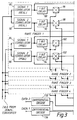
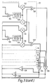
- FIG. 2 A block diagram for two equal amplitude, equal rate, signals is shown in Figure 3.
- Rake fingers 72, 74, 76, 78 each of which comprise first and second signal correlators 80, 82 for handling the inphase signal components received from a down converter and third and fourth correlators 84, 86 for handling the quadrature phase components of an input signal similarly received from a down converter.
- An output from the signal correlater 80 is connected to an input of a one bit delay circuit 88 and to a first input of a multiplier 112.
- An output from the one bit delay circuit 88 is connected to an input of a half linear multiplier 96, the output of which is connected to an adder circuit 104.
- the output of the correlator 82 is connected to an input of a one bit delay circuit 90 and to a first input of a multiplier 114.
- the output from the one bit delay circuit 90 is connected to a first input of a half linear multiplier 98, the output of which is connected to a further input of the adder circuit 104.
- the output of the adder circuit 104 is connected to an input of a Wiener filter 108, the output of which is connected to a second input of the multipliers 112, 114.
- the signal correlater 84 has an output connected to a one bit delay circuit 92 and to a first input of a multiplier 116.
- An output from the one bit delay circuit 92 is connected to a first input of a half linear multiplier 100, the output of which is connected to an input of an adder circuit 106.
- the output of the adder circuit 106 is connected to an input of a Wiener filter 110, the output of which is connected to second inputs of the multipliers 116 and 118.
- the signal correlater 86 has an output connected to an input of a one bit delay circuit 94 and to a first input of the multiplier 118.
- An output from the one bit delay circuit 94 is connected to an input of a half linear multiplier 102, the output of which is connected to a further input of the adder circuit 106.
- An output from the multipliers 112, 116 are connected to a respective input of an adder circuit 120, and the outputs from the multipliers 114, 118 are connected to a respective input of an adder circuit 122.
- the circuitry described so far is repeated in each of the Rake fingers.
- the output from the adder circuit 120 and the respective outputs from the other Rake fingers are applied to an adder circuit 126 and the outputs from the adder circuit 122 and the other adder circuits in the Rake fingers are applied to an input of an adder circuit 124.
- the output from the adder circuit 126 is connected to a hard limiting device 130, the output of which is fed back to a second input of the half linear multipliers 96, 100 in each Rake finger.
- the output of the adder circuit 124 is applied to a hard limiting circuit 128, the output of which is fed back to the half linear multipliers 98, 102 in each Rake finger.
- the outputs of the adder circuits 124, 126 are also applied to a respective differential decode circuit 132, 134 respectively from which the output data is generated for each signal.
- the two signals are de-spread independently, decision corrected independently and added together to feed to the input of the channel estimation filter, that is the Wiener filters 108, 110.
- the Wiener filters 108, 110 For demodulation of equal rate signals received over the same paths this results in an approximate 3dB reduction in the mean square error for the channel estimates.
- receivers for more than two signals could be combined. It will also be appreciated that the architectures of Figures 2 and 3 could readily be combined so that pilot estimation could be achieved over any equal bit rates but applied to m > n signals where the additional signals for demodulation all had a significantly lower bit rate.
- Figure 3 can conveniently be modified as shown in Figure 4 and therefore like circuit elements have been given the same designation.
- the difference between Figures 3 and 4 is the inclusion of the sample blocks 136 and 138 between the output of the half linear multiplier 96 and the input of the adder 104, and the output of the half linear multiplier 100 and the input of the adder circuit 106, respectively.
- These blocks add together samples of the higher bit rate signalling in blocks of k samples prior to input to the Wiener filter 108, 110 respectively, in this way the rates of inputs to the adders 104, 106 respectively are matched.
- the accumulation effectively weights the high bit rate signal (stronger signal) in proportional to its amplitude in such a way that the optimum benefit is obtained from combination across the signals.
- k bit rate ratio
- any of the above embodiments may be implemented using a pre-combining Rake architecture, and may be used for decision directed reference extraction and for the demodulation of multiple signals.
- the architecture which achieves this is shown in Figure 5.
- Figure 5 is very similar to Figure 1 and like circuit elements have been given the same reference numeral.
- the output from the adder circuit 40 is connected to a respective input of the signal correlators 48, 150, 154 which handles the signals 1, 2 and 3 respectively.
- An output from each correlator is fed to an input of a differential decode circuit 46, 152, 156 from which the data output is taken from a respective output line.
- the inputs for the half linear multipliers 26, 28 are taken from the output of the correlator 48 and is similarly fed via a hard limiting circuit 42 and a latch circuit 44.
- the outputs from each Rake finger are therefore at the chip rate rather than the bit rate.
- an additional correlator is required in order to demodulate signal 1 following the overall combiner.
- Figure 5 could be combined with that of Figure 3 or 4 to enable the pre-combining to be performed on the basis of more than one signal whilst allowing multiplicity of additional lower bit rate signals to be demodulated.
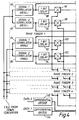
- Figure 6 The architecture for the case of combining Figure 5 with Figure 3 is illustrated in Figure 6, and like circuit elements have been given the same reference numeral.
- the difference between the Rake fingers of Figure 3 and Figure 6 is that the output of the Wiener filters 108, 110 are applied to a first input of a multiplier 112, 116 respectively.
- the second input of the multipliers 112, 116 receive the inphase and quadrature phase components of the input signal from the down converter respectively.
- the outputs from the Rake fingers are summed by the adder circuit 40, the output of which is applied to an input of a plurality of signal correlators 48, 150, 154 and 158 handling signals 1 to 4 respectively.
- the output of the signal correlators 154 and 158 are applied to an input of a differential decode circuit 156, 160 respectively from which the data signals 3 and 4 are generated.
- the output signals from the signal correlators 48 and 150 are applied to a hard limiting device 42, 162 respectively and to the differential decode circuits 46, 152 respectively from which the data signals 1 and 2 are generated.
- the output signals from the hard limiting devices 42, 162 are applied to a respective latch circuit 44, 162.
- the output of the latch circuit 44 is applied to the second input of the half linear multipliers 96 and 100 in each Rake finger, and similarly the output of the latch circuit 164 is applied to the second input of the half linear multipliers 98, 102 in each Rake finger.
- the signals 1 and 2 are both transmitted at the same bit rate which is higher than the rate of signals 3 and 4.
- the channel estimates are formed on the basis of decision directed demodulation of signals 1 and 2 and are then used for the purpose of rate pre-combining.
- the pre-combined signal can then be readily de-spread for demodulating of additional signals such as signals 3 and 4.
Landscapes
- Engineering & Computer Science (AREA)
- Computer Networks & Wireless Communication (AREA)
- Signal Processing (AREA)
- Digital Transmission Methods That Use Modulated Carrier Waves (AREA)
- Mobile Radio Communication Systems (AREA)
Applications Claiming Priority (2)
| Application Number | Priority Date | Filing Date | Title |
|---|---|---|---|
| GB9317781 | 1993-08-26 | ||
| GB9317781A GB2281482B (en) | 1993-08-26 | 1993-08-26 | Apparatus for use in equipment providing a digital radio link between a fixed and a mobile radio unit |
Publications (2)
| Publication Number | Publication Date |
|---|---|
| EP0641091A1 true EP0641091A1 (de) | 1995-03-01 |
| EP0641091B1 EP0641091B1 (de) | 2002-03-20 |
Family
ID=10741088
Family Applications (1)
| Application Number | Title | Priority Date | Filing Date |
|---|---|---|---|
| EP94110653A Expired - Lifetime EP0641091B1 (de) | 1993-08-26 | 1994-07-08 | Vorrichtung mit entscheidungsgesteuerter Kanalschätzung in einer digitalen Mobilfunkverbindung |
Country Status (7)
| Country | Link |
|---|---|
| US (1) | US5594755A (de) |
| EP (1) | EP0641091B1 (de) |
| JP (1) | JPH0786985A (de) |
| CN (1) | CN1108835A (de) |
| DE (1) | DE69430160T2 (de) |
| GB (1) | GB2281482B (de) |
| IN (1) | IN188216B (de) |
Cited By (5)
| Publication number | Priority date | Publication date | Assignee | Title |
|---|---|---|---|---|
| WO1997004536A1 (en) * | 1995-07-19 | 1997-02-06 | Ericsson Inc. | Method and apparatus for spread-spectrum channel estimation |
| WO1998011676A3 (en) * | 1996-09-13 | 1998-05-14 | Ericsson Telefon Ab L M | Coherent demodulation with decision-directed channel estimation for digital communication |
| WO2000046935A1 (en) * | 1999-02-08 | 2000-08-10 | Qualcomm Incorporated | Method and apparatus for time tracking |
| EP0849887A3 (de) * | 1996-12-17 | 2000-11-08 | Lucent Technologies Inc. | Schaltung und Verfahren zum Nachführen von Fingerverschiebung in einem Spreizspektrum RAKE-Empfänger |
| CN101232304B (zh) * | 2008-02-29 | 2012-05-30 | 北京邮电大学 | 一种通信系统中发送和接收信道信息的方法和设备 |
Families Citing this family (7)
| Publication number | Priority date | Publication date | Assignee | Title |
|---|---|---|---|---|
| GB2293730B (en) * | 1994-09-28 | 1998-08-05 | Roke Manor Research | Apparatus for use in equipment providing a digital radio link between a fixed and a mobile radio unit |
| FI97581C (fi) * | 1995-02-10 | 1997-01-10 | Nokia Telecommunications Oy | Vastaanotin ja menetelmä hajotuskoodien generoimiseksi vastaanottimessa |
| US5764688A (en) * | 1995-06-30 | 1998-06-09 | Roke Manor Research Limited | Apparatus for use in equipment providing a digital radio link between a fixed and a mobile radio unit |
| US5983105A (en) * | 1997-03-17 | 1999-11-09 | Nokia Telecommunications Oy | Method and receiver implemented on the rake principle |
| JP2870526B1 (ja) * | 1997-09-04 | 1999-03-17 | 日本電気株式会社 | Cdma受信装置 |
| FR2814877B1 (fr) * | 2000-10-02 | 2003-01-03 | Mitsubishi Electric Inf Tech | Sequence d'estimation de canal et procede d'estimation d'un canal de transmission qui utilise une telle sequence d'estimation de canal |
| KR100427577B1 (ko) * | 2001-12-27 | 2004-04-28 | 한국전자통신연구원 | 하드웨어 복잡도를 줄인 레이크 수신기 |
Family Cites Families (3)
| Publication number | Priority date | Publication date | Assignee | Title |
|---|---|---|---|---|
| US5519730A (en) * | 1990-06-12 | 1996-05-21 | Jasper; Steven C. | Communication signal having a time domain pilot component |
| JPH07509113A (ja) * | 1993-05-12 | 1995-10-05 | ロウク マナー リサーチ リミテッド | 固定無線ユニットと移動無線ユニットとの間のデジタル無線リンクの形成用設備向け装置 |
| US5361276A (en) * | 1993-09-13 | 1994-11-01 | At&T Bell Laboratories | All digital maximum likelihood based spread spectrum receiver |
-
1993
- 1993-08-26 GB GB9317781A patent/GB2281482B/en not_active Expired - Fee Related
-
1994
- 1994-07-08 EP EP94110653A patent/EP0641091B1/de not_active Expired - Lifetime
- 1994-07-08 DE DE69430160T patent/DE69430160T2/de not_active Expired - Fee Related
- 1994-08-05 IN IN743MA1994 patent/IN188216B/en unknown
- 1994-08-18 US US08/292,040 patent/US5594755A/en not_active Expired - Fee Related
- 1994-08-26 CN CN94115732.6A patent/CN1108835A/zh active Pending
- 1994-08-26 JP JP6202343A patent/JPH0786985A/ja active Pending
Non-Patent Citations (6)
| Title |
|---|
| J.G. PROAKIS:: "Digital Communications. 2nd Edition.", 1989, MCGRAW-HILL, NEW YORK, US * |
| R.A. ILTIS / S.H. GOLDBERG:: "A DS Spread Spectrum RAKE Receiver With Narrowband Interference Rejection Capability: Operation in Fading Channels.", MILCOM '89. 1989 IEEE MILITARY COMMUNICATIONS CONFERENCE, 15.-18.10.1989, BOSTON, US, vol. 1, 15 October 1989 (1989-10-15), IEEE, NEW YORK, US, pages 704 - 708, XP000131901 * |
| R.A. ILTIS:: "A GLRT-Based Spread-Spectrum Receiver for Joint Channel Estimation and Interference Suppression.", IEEE TRANSACTIONS ON COMMUNICATIONS, vol. 37, no. 3, March 1989 (1989-03-01), NEW YORK US, pages 277 - 288, XP000039434 * |
| T. MIYATANI / Y. AKAIWA:: "A Spread Spectrum Communication System without Reference Signal for Frequency-Selective Fading Channel.", 43RD IEEE VEHICULAR TECHNOLOGY CONFERENCE, 18.-20.05.1993, SECAUCUS, US, 18 May 1993 (1993-05-18), IEEE, NEW YORK, US, pages 835 - 838, XP000393311 * |
| V.-P. KAASILA / A. MÄMMELÄ:: "The Adaptive RAKE Matched Filter in a Time-Variant Two-Path Channel.", PIMRC '92. IEEE INTERNATIONAL SYMPOSIUM ON PERSONAL, INDOOR AND MOBILE RADIO COMMUNICATIONS PROCEEDINGS, 19.-21.10.1992, BOSTON, US, 19 October 1992 (1992-10-19), IEEE, NEW YORK, US, pages 441 - 445, XP010107055, DOI: doi:10.1109/PIMRC.1992.279891 * |
| Y. SANADA / A. KAJIWARA / M. NAKAGAWA:: "Adaptive RAKE Receiver for Mobile Communications.", IEICE TRANSACTIONS ON COMMUNICATIONS, vol. E76-B, no. 8, August 1993 (1993-08-01), TOKYO JP, pages 1002 - 1007, XP000396905 * |
Cited By (7)
| Publication number | Priority date | Publication date | Assignee | Title |
|---|---|---|---|---|
| WO1997004536A1 (en) * | 1995-07-19 | 1997-02-06 | Ericsson Inc. | Method and apparatus for spread-spectrum channel estimation |
| US5677930A (en) * | 1995-07-19 | 1997-10-14 | Ericsson Inc. | Method and apparatus for spread spectrum channel estimation |
| WO1998011676A3 (en) * | 1996-09-13 | 1998-05-14 | Ericsson Telefon Ab L M | Coherent demodulation with decision-directed channel estimation for digital communication |
| US5768307A (en) * | 1996-09-13 | 1998-06-16 | Telefonaktiebolaget Lm Ericsson | Coherent demodulation with decision-directed channel estimation for digital communication |
| EP0849887A3 (de) * | 1996-12-17 | 2000-11-08 | Lucent Technologies Inc. | Schaltung und Verfahren zum Nachführen von Fingerverschiebung in einem Spreizspektrum RAKE-Empfänger |
| WO2000046935A1 (en) * | 1999-02-08 | 2000-08-10 | Qualcomm Incorporated | Method and apparatus for time tracking |
| CN101232304B (zh) * | 2008-02-29 | 2012-05-30 | 北京邮电大学 | 一种通信系统中发送和接收信道信息的方法和设备 |
Also Published As
| Publication number | Publication date |
|---|---|
| CN1108835A (zh) | 1995-09-20 |
| EP0641091B1 (de) | 2002-03-20 |
| GB9317781D0 (en) | 1993-10-13 |
| GB2281482B (en) | 1997-10-22 |
| IN188216B (de) | 2002-08-31 |
| DE69430160D1 (de) | 2002-04-25 |
| JPH0786985A (ja) | 1995-03-31 |
| US5594755A (en) | 1997-01-14 |
| GB2281482A (en) | 1995-03-01 |
| DE69430160T2 (de) | 2002-10-31 |
Similar Documents
| Publication | Publication Date | Title |
|---|---|---|
| EP0671082B2 (de) | Datenmultiplixierer für mehrwegempfänger | |
| US5383220A (en) | Data demodulator of a receiving apparatus for spread spectrum communication | |
| US6097712A (en) | Multi-carrier CDMA communications systems | |
| EP0882333B1 (de) | Verfahren und anordnung zur signaldemodulation und diversitykombination orthogonal modulierter signale | |
| KR19980032939A (ko) | 간섭신호 제거장치 | |
| US5594755A (en) | Apparatus for use in equipment providing a digital radio link between a fixed radio unit and a mobile radio unit | |
| US5910950A (en) | Demodulator phase correction for code division multiple access receiver | |
| US5809062A (en) | Ambiguity resolution system in direct sequence spread spectrum modulation systems | |
| EP1176733A1 (de) | Empfänger und empfangsverfahren für spreizspektrumübertragung | |
| EP1229667A2 (de) | Auswahl von mehreren Übertragungswegen durch sukzessives enfernen und detektieren von hohen Autokorrelationen | |
| US7027491B2 (en) | Interference cancellation receiver for use in a CDMA system | |
| US20020009128A1 (en) | Receiving apparatus | |
| EP0650646A1 (de) | Zweistufig arbeitender "rake"-empfanger in einer digitalen funkverbindung zwischen einer ortsfesten und mobilen funkstation | |
| GB2278029A (en) | Apparatus for use in digital radio equipment | |
| HK1011126B (en) | Dot product circuit multipath receivers | |
| MXPA98006794A (en) | Method and apparatus for the demodulation of signal and the combination in diversity of modulated signals ortogonalme | |
| MXPA99004498A (en) | Despreading of direct sequence spread spectrum communications signals | |
| JPH06152563A (ja) | 逆拡散装置 |
Legal Events
| Date | Code | Title | Description |
|---|---|---|---|
| PUAI | Public reference made under article 153(3) epc to a published international application that has entered the european phase |
Free format text: ORIGINAL CODE: 0009012 |
|
| AK | Designated contracting states |
Kind code of ref document: A1 Designated state(s): DE ES FR GB IT |
|
| 17P | Request for examination filed |
Effective date: 19950711 |
|
| 17Q | First examination report despatched |
Effective date: 19990705 |
|
| GRAG | Despatch of communication of intention to grant |
Free format text: ORIGINAL CODE: EPIDOS AGRA |
|
| GRAG | Despatch of communication of intention to grant |
Free format text: ORIGINAL CODE: EPIDOS AGRA |
|
| GRAG | Despatch of communication of intention to grant |
Free format text: ORIGINAL CODE: EPIDOS AGRA |
|
| GRAH | Despatch of communication of intention to grant a patent |
Free format text: ORIGINAL CODE: EPIDOS IGRA |
|
| GRAH | Despatch of communication of intention to grant a patent |
Free format text: ORIGINAL CODE: EPIDOS IGRA |
|
| REG | Reference to a national code |
Ref country code: GB Ref legal event code: IF02 |
|
| GRAA | (expected) grant |
Free format text: ORIGINAL CODE: 0009210 |
|
| AK | Designated contracting states |
Kind code of ref document: B1 Designated state(s): DE ES FR GB IT |
|
| REF | Corresponds to: |
Ref document number: 69430160 Country of ref document: DE Date of ref document: 20020425 |
|
| PGFP | Annual fee paid to national office [announced via postgrant information from national office to epo] |
Ref country code: GB Payment date: 20020703 Year of fee payment: 9 |
|
| PGFP | Annual fee paid to national office [announced via postgrant information from national office to epo] |
Ref country code: FR Payment date: 20020709 Year of fee payment: 9 |
|
| PGFP | Annual fee paid to national office [announced via postgrant information from national office to epo] |
Ref country code: DE Payment date: 20020717 Year of fee payment: 9 |
|
| ET | Fr: translation filed | ||
| ET | Fr: translation filed | ||
| PG25 | Lapsed in a contracting state [announced via postgrant information from national office to epo] |
Ref country code: ES Free format text: LAPSE BECAUSE OF FAILURE TO SUBMIT A TRANSLATION OF THE DESCRIPTION OR TO PAY THE FEE WITHIN THE PRESCRIBED TIME-LIMIT Effective date: 20020925 |
|
| PLBE | No opposition filed within time limit |
Free format text: ORIGINAL CODE: 0009261 |
|
| STAA | Information on the status of an ep patent application or granted ep patent |
Free format text: STATUS: NO OPPOSITION FILED WITHIN TIME LIMIT |
|
| 26N | No opposition filed |
Effective date: 20021223 |
|
| PG25 | Lapsed in a contracting state [announced via postgrant information from national office to epo] |
Ref country code: GB Free format text: LAPSE BECAUSE OF NON-PAYMENT OF DUE FEES Effective date: 20030708 |
|
| PG25 | Lapsed in a contracting state [announced via postgrant information from national office to epo] |
Ref country code: DE Free format text: LAPSE BECAUSE OF NON-PAYMENT OF DUE FEES Effective date: 20040203 |
|
| GBPC | Gb: european patent ceased through non-payment of renewal fee |
Effective date: 20030708 |
|
| PG25 | Lapsed in a contracting state [announced via postgrant information from national office to epo] |
Ref country code: FR Free format text: LAPSE BECAUSE OF NON-PAYMENT OF DUE FEES Effective date: 20040331 |
|
| REG | Reference to a national code |
Ref country code: FR Ref legal event code: ST |
|
| PG25 | Lapsed in a contracting state [announced via postgrant information from national office to epo] |
Ref country code: IT Free format text: LAPSE BECAUSE OF NON-PAYMENT OF DUE FEES;WARNING: LAPSES OF ITALIAN PATENTS WITH EFFECTIVE DATE BEFORE 2007 MAY HAVE OCCURRED AT ANY TIME BEFORE 2007. THE CORRECT EFFECTIVE DATE MAY BE DIFFERENT FROM THE ONE RECORDED. Effective date: 20050708 |