EP0641107A2 - ATM-Zellenvermittlungssystem - Google Patents
ATM-Zellenvermittlungssystem Download PDFInfo
- Publication number
- EP0641107A2 EP0641107A2 EP94305579A EP94305579A EP0641107A2 EP 0641107 A2 EP0641107 A2 EP 0641107A2 EP 94305579 A EP94305579 A EP 94305579A EP 94305579 A EP94305579 A EP 94305579A EP 0641107 A2 EP0641107 A2 EP 0641107A2
- Authority
- EP
- European Patent Office
- Prior art keywords
- cells
- cell
- output
- input
- cell switching
- Prior art date
- Legal status (The legal status is an assumption and is not a legal conclusion. Google has not performed a legal analysis and makes no representation as to the accuracy of the status listed.)
- Withdrawn
Links
- 230000015654 memory Effects 0.000 claims description 31
- 239000000872 buffer Substances 0.000 claims description 17
- 238000012546 transfer Methods 0.000 claims description 3
- 238000000034 method Methods 0.000 description 7
- 238000010586 diagram Methods 0.000 description 4
- 239000000284 extract Substances 0.000 description 3
- 230000005540 biological transmission Effects 0.000 description 2
- 230000006870 function Effects 0.000 description 2
- 238000004891 communication Methods 0.000 description 1
- 238000011156 evaluation Methods 0.000 description 1
- 238000012986 modification Methods 0.000 description 1
- 230000004048 modification Effects 0.000 description 1
Images


Classifications
-
- H—ELECTRICITY
- H04—ELECTRIC COMMUNICATION TECHNIQUE
- H04L—TRANSMISSION OF DIGITAL INFORMATION, e.g. TELEGRAPHIC COMMUNICATION
- H04L12/00—Data switching networks
- H04L12/54—Store-and-forward switching systems
- H04L12/56—Packet switching systems
- H04L12/5601—Transfer mode dependent, e.g. ATM
-
- H—ELECTRICITY
- H04—ELECTRIC COMMUNICATION TECHNIQUE
- H04L—TRANSMISSION OF DIGITAL INFORMATION, e.g. TELEGRAPHIC COMMUNICATION
- H04L49/00—Packet switching elements
- H04L49/10—Packet switching elements characterised by the switching fabric construction
- H04L49/104—Asynchronous transfer mode [ATM] switching fabrics
- H04L49/105—ATM switching elements
- H04L49/107—ATM switching elements using shared medium
-
- H—ELECTRICITY
- H04—ELECTRIC COMMUNICATION TECHNIQUE
- H04L—TRANSMISSION OF DIGITAL INFORMATION, e.g. TELEGRAPHIC COMMUNICATION
- H04L49/00—Packet switching elements
- H04L49/15—Interconnection of switching modules
- H04L49/1553—Interconnection of ATM switching modules, e.g. ATM switching fabrics
-
- H—ELECTRICITY
- H04—ELECTRIC COMMUNICATION TECHNIQUE
- H04Q—SELECTING
- H04Q11/00—Selecting arrangements for multiplex systems
- H04Q11/04—Selecting arrangements for multiplex systems for time-division multiplexing
- H04Q11/0428—Integrated services digital network, i.e. systems for transmission of different types of digitised signals, e.g. speech, data, telecentral, television signals
- H04Q11/0478—Provisions for broadband connections
-
- H—ELECTRICITY
- H04—ELECTRIC COMMUNICATION TECHNIQUE
- H04L—TRANSMISSION OF DIGITAL INFORMATION, e.g. TELEGRAPHIC COMMUNICATION
- H04L12/00—Data switching networks
- H04L12/54—Store-and-forward switching systems
- H04L12/56—Packet switching systems
- H04L12/5601—Transfer mode dependent, e.g. ATM
- H04L2012/5638—Services, e.g. multimedia, GOS, QOS
- H04L2012/5646—Cell characteristics, e.g. loss, delay, jitter, sequence integrity
- H04L2012/565—Sequence integrity
-
- H—ELECTRICITY
- H04—ELECTRIC COMMUNICATION TECHNIQUE
- H04L—TRANSMISSION OF DIGITAL INFORMATION, e.g. TELEGRAPHIC COMMUNICATION
- H04L12/00—Data switching networks
- H04L12/54—Store-and-forward switching systems
- H04L12/56—Packet switching systems
- H04L12/5601—Transfer mode dependent, e.g. ATM
- H04L2012/5678—Traffic aspects, e.g. arbitration, load balancing, smoothing, buffer management
- H04L2012/5681—Buffer or queue management
Definitions
- the present invention relates to an ATM (Asynchronous Transfer Mode) cell switching system, more especially one in which information such as voices, data, images are divided into each fixed length of cell and switched at a very high speed, and in particular relates to an ATM cell switching system capable of realizing a cell sequence control in the switching process using a simplified method.
- ATM Asynchronous Transfer Mode
- a cell distributing means provided corresponding to an input port, a plurality of cell switching means, and a cell sequential aligning means provided corresponding to an output port, where the cell distributing means selects one cell switching means from among said plurality of cell switching means, and outputs the cell given of the time stamp showing the input time to the cell switching means, said plurality of cell switching means perform the switching processes, the cell sequential aligning means outputs to the output port after aligning the cell output sequence using the time stamp given to the cell.
- the conventional cell switching system is described as to its structure and operation using block diagrams in Figs. 4, 5, and 6 in the present application, assuming that two input lines are provided and a cell switching device is formed of two switch circuits.
- Fig. 4 shows the cell switching device, wherein 400a, 400b depicts a cell distributing circuit, 401a, 401b switch circuits receiving outputs of the cell distributing circuits 400a, 400b as inputs respectively, and 402a, 402b cell sequence aligning circuits receiving outputs of the switch circuits 401a, 401b as inputs.
- Fig. 5 shows the switch circuit, wherein 501 depicts a time division multiplex bus, 502a, 502b address filters connected to the time division multiplex bus 501, and 503a, 503b FIFO (First In First Out) buffers receiving outputs of the address filters 502a and 502b as inputs respectively.
- 501 depicts a time division multiplex bus
- 503a, 503b FIFO (First In First Out) buffers receiving outputs of the address filters 502a and 502b as inputs respectively.
- FIFO First In First Out
- Fig. 6 shows the cell sequence aligning means, wherein 601a, 601b depict cell sequence aligning memories, and 602 a time stamp minimum value detecting circuit performing outputting and inputting between the cell sequence aligning memories 601a, 601b in respect of information.
- Figs. 4 to 6 designate examples of circuit operation.
- the cell input from the input port is, at the cell distributing means 400a, 400b, given of the time stamp showing the input time, and is output to one switch circuit selected from a plurality of switch circuits.
- the cell from the cell distributing means 400a, 400b is switched in accordance with address information given to the cell at the switch circuits 401a, 401b, and is output to the cell sequence aligning circuits 402a, 402b which is connected to the desired output ports.
- the cell sequence aligning circuits 402a, 402b output the cells to the output ports depending on the time stamp provided on the cell.
- the switch circuit has a structure as shown in Fig. 5.
- the cell input from each input port of the switch circuit 500 is multiplexed in time division at the time division multiplex bus 501, and is input in a time divisional manner into the address filters 502a, 502b corresponding to each output port.
- the address filters 502a, 502b detect headers of the cells, subtract only the desirous cells, and output them to FIFO buffers 503a, 503b, which store and output the cells in a manner of "first in first out".
- the cells output from each switch circuit are stored in the cell sequence aligning memories 601a, 601b, provided at every switch circuit basis, which store and output the cells in way of first in first out.
- the time stamp minimum value detecting circuit 602 compares the time stamps given to the cells stored in the head part of the cell sequence aligning memories 601a, 601b, to detect the smallest time-stamp, and to transmit control signals so that the cell having the smallest time-stamp is to be output from the cell sequence aligning memories 601a, 601b.
- An aim of the invention is to provide an ATM cell exchange system capable of realizing a cell sequence control by a simplified method without using time stamp.
- An ATM cell switching system in a cell switching system having a plurality of input ports and a plurality of output ports in which cells of a fixed length packet input from said plurality of input ports are output from the desired output ports in accordance with address information added to such cells, is characterized by comprising, a cell distributing section, a cell switching section, and a cell output control section, and further oharacterised in that;
- the cell distributing section provided corresponding to the input ports has one input line connected to one of said plurality of input ports and a plurality of output lines, sequentially selects one output line from said plurality of output lines, separates cells input from the input ports into each cell unit, and outputs to the selected output line;
- the cell switching sections arranged in the same number corresponding to output lines of the cell distributing section have a plurality of input lines and a plurality of output lines, said plurality of input lines being connected respectively to the different output lines of the cell distributing section to detect address information added to each cell, the cell switching sections output cells towards
- the cell switching section in the ATM cell switching system of the present invention is characterized by comprising; a time division selector accommodating a plurality of input lines of the cell switching section, selecting the cells input from each input line in time divisional manner to distribute into a plurality of output lines by the time division multiplexing; an address filter provided corresponding to the output port, receiving the cells output from the time division selector, discriminating address information added to each cell, receiving and passing only the cells to be routed to the output ports corresponding to its own output ports, obtaining the number of cells received and passed through at the same time, and transmitting such information of the number of cells and the identifier indicating its own cell switching section to the cell output control section; a first-in-first-out (FIFO) buffer provided corresponding to the address filter, storing the cells passed through such address filter at the arrived order, and outputting thus stored cells one by one at the arrived order to the output ports in accordamce with the instruction of the cell output control section.
- a time division selector accommodating a plurality of input lines of the
- the cell output control section in the ATM cell switching system of the present invention is characterized by comprising; a number of cells storage memory receiving a number of cells towards the same output line at the same time transmitted from the cell switching section and an identifier indicating the cell switching section, and storing such information at the received order; a decoder recognizing the identifier of the information stored in the head part of the number of cells storage memory, and instructing a cell switching section corresponding to its identifier to output one cell to the output port; a number of cells storage subtracting section reading the a value of number of cells stored in the head part of the number of cells storage memory, subtracting 1 from a value of such number of cells, in which if a value of thus subtracted number of cells reaches 0, the corresponding information of number of cells and the identifier is discarded, and if a value of thus subtracted number of cells does not reach 0, the corresponding number of cells is replaced by the subtracted value.
- the ATM cell switching system of the present invention can perform sequence aligning control of the cells in accordance with the number of cells, towards the same output direction at the same time, calculated at every address filter basis of each cell switching section, without giving the time stamp indicating the input time of each cell.
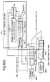
- Fig. 1 is a block diagram showing one embodiment of an asynchronous transfer mode (ATM) cell switching system according to the present invention, which is a basic structure illustrating a principle of the invention.
- ATM asynchronous transfer mode
- 100a, 100b depict cell distributing sections, which are provided corresponding to the input ports and have functions in that a plurality of cells input from the input ports are separated into each cell unit, one input line and a plurality of output lines are provided therein, the input line is connected to the input port, one output line is sequentially selected from said plurality of output lines, the cells input from the input ports are output to the thus selected one output line.
- Numerals 101a, 101b depict cell switching sections, which are provided in a number equal to the number of output lines of the cell distributing sections 100a, 100b.
- the cell switching section has a plurality of input lines and a plurality of output lines, said plurality of input lines being connected to output lines of different cell distributing sections respectively, and detects address information of thus input cell, whereby the cells towards the same output line are output to the output line in the manner of the cell input sequence keeping such sequence order.
- the cell switching section functionally obtains the number of cells toward the same output line at the same time for each output line basis, and transmits such information to the cell output control section.
- Numerals 105a, 105b depict output control sections, provided corresponding to the output ports, whose plurality of inputs are connected to different cell switching sections 101a, 101b respectively.
- the output control section is formed of a number of cells storage memory 108, a number of cells storage subtracting section 106, and a number of cells storage comparator 109.
- the number of cells storage comparator 109 receives the number of cells toward the same output line at the same time from the cell switching section together with an identifier designating such cell switching section, and if the number of cells is greater than zero, it is input into the number of cell storage memory 108.
- the number of cells storage subtracting section 106 extracts both the number of cells which has fastest been input into the number of cells storage memory 108, and an identifier corresponding to such number of cells, and transmits a request of cell output to the cell switching section designated by the identifier corresponding to such information of number of cells, the value of number of cells is subtracted by one, and if the subtracted value is less than zero, such information of number of cells and corresponding identifier is discarded from the number of cells storage memory 108, and if the subtracted value is more than zero, such number of cells is replaced with that subtracted value.
- the cell distributing sections 100a, 100b may preferably have a function that a plurality of cells coming from the input ports are separated into a cell unit, each output direction of cells can sequentially be changed, and, in addition, the cell distributing sections corresponding to all the input ports are synchronously operated.
- Each cell switching section 101a, 101b includes a time division selector 102, address filters 103a, 103b and FIFO buffers 104a, 104b.
- the time division selector 102 which is connected to each input line of the corresponding cell switching section, selects the cells input from each input line in time divisional manner, to multiplex in time division, and to distribute into a plurality of outputs.
- the address filters 103a, 103b provided corresponding to each output port, whose each input is connected to the time division selector 102, receive the cells output from the time division selector 102 to discriminate address information of those cells which will be output to the corresponding output ports.
- Futhermore the number of cells, toward the same output port, which has arrived at the time division selector 102 at the same time, are obtained and transmitted to the output control sections 105a, 105b.
- FIFO buffers 104a, 104b whose each input is connected to the address filters 103a, 103b, store the cells received by the address filters 103a, 103b, and output them to the output ports.
- the cell switching sections 101a, 101b are structured output buffer type cell switches having the cell buffers corresponding to each output port.
- both structures may preferably be available; namely, a common buffer type switch which the cell buffer corresponding to each output port is commonly used for all the output ports; and a cross point type switch having buffers at each cross point of input and output.
- Each output control section 105a, 105b includes the number of cells storage comparator 109, the number of cells storage memory 108, a decoder 107, and the number of cells storage subtracting section 106.
- the input of the number of cells storage comparator 109 is connected to both of the number of cells indicating signal output from the address filters 103a, 103b of the cell switching sections 101a, 101b and the identifier signal output from the cell switching sections 101a, 101b, and selectively receives the numnber of cells indicating signal whose value is greater than zero in time division manner together with the identifier of the cell switching section which have processed those cells.
- the number of cells storage memory 108 is connected on its input with an output of the number of cells storage comparator 109, and stores and outputs the cell storage number output from the number of cells storage comparator 109 and the identifier of the cell switching section.
- the decoder 107 is connected on its input with an output of the number of cells storage memory 108, and in accordance with an identifier of the cell switching section output from the number of cells storage memory 108, a cell transmission request signal to the FIFO buffer 104a of the cell switching sections 101a, 101b is produced.
- the number of cells storage subtracting section 106 is connected on its input with the output of the number of cells storage memory 108, the value of the number of cells output from the number of cells storage memory 108 is subtracted by one, and if the value of the number of cells comes to zero, then the information of the number of cells which has fastest been input into the number of cells storage memory 108 from the number of cells storage comparator 109 and the identifier of the cell switching section is discarded, and in cases other than described above, the number of cells storage memory 108 is controlled in that the information of the number of cells which has fastest been input into the number of cells storage memory 108 from the number of cells storage comparator 109 is replaced by the value of the number of cells having been subtracted.
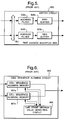
- Figs. 2 and 3 show a cell switching section of Fig. 1, illustrating a basic operation of an output control section
- Fig. 2 is an operation example relating to input ports to address filters
- Fig. 3 is an operation example of the output control section.
- the cells input from the input ports are all towards the output port #1.
- the cells input from the input ports are separated into each cell unit by cell distributing sections 200a, 200b.
- an input speed to each cell switching section 201a, 201b comes to the line speed of the input port / the number of cell switching sections.
- the cells input into the cell switching sections 201a, 201b are multiplexed by the time division selector 202, and are output to each address filter 203a, 203b.
- the address filters 203a and 203b which are provided corresponding to the output ports, extracts only desired cell towards the corresponding output port to output it to the FIFO buffer. From among the cells input into the time division selector 202 at the same time during the gate being opened, the number of cells extracted by its own address filter and the identifier showing its own cell switching section both are output to the output control section.
- Fig. 3(A) in an output control section 307, the information of the identifier of the cell switching section which has fastest been input in the number of cells storage memory 304 in which the information of the number of cells and the identifier indicating a cell switching section is being stored in accordance with output of address filters 300a, 300b is extracted, and the cell output request signal is sent to FIFO buffers 301a or 301b of the corresponding cell switching section.
- the value of the number of cells is extracted from the number of cells storage memory 304, and after subtracting by one, the value before subtracting in respect of the number of cells storage memory 304 is renewed by the subtracted value. However, if the subtracted value is equal to zero as shown in Fig. 3(B), the value before subtraction together with the identifier of the cell switching section is discarded.
- the buffers of the cell switching sections 302a, 302b perform storage and output of the cell in accordance with the rule of FIFO.
- the number of cells storage memory 304 stores both the identifier of the cell switching section and the cell number with reference to an inputted sequence ranging all the cell switching sections 302a, 302b, whereby the output controls of the cell switching sections 302a, 302b are performed. This provides an output from the buffers of the cell switching section while maintaining a cell sequence normal.
- 300a, 300b depict address filters, 303 a number of cells storage comparator receiving outputs of the address filters 300a, 300b as inputs, 305 a decoder having an input of a cell switching section identifier 308 of the number of cells storage memory 304.
- the decoder 305 sends a cell output request to the buffers 301a, 301b of FIFO.
- Numeral 306 depicts a number of cells storage subtracting section receiving a stored number of cells 309 of the number of cells storage memory 304 as an input, and 307 an output control section for containing those described above.
- the present invention is capable of realizing a cell sequence control by a simplified method without using time stamp because the number of cells directing to the same output at the same time for each address filter basis of each cell switching section is calculated to perform the sequence aligning control of the cells in accordance with such calculated values.
Landscapes
- Engineering & Computer Science (AREA)
- Computer Networks & Wireless Communication (AREA)
- Signal Processing (AREA)
- Data Exchanges In Wide-Area Networks (AREA)
Applications Claiming Priority (2)
| Application Number | Priority Date | Filing Date | Title |
|---|---|---|---|
| JP20687693A JP2629568B2 (ja) | 1993-07-30 | 1993-07-30 | Atmセル交換方式 |
| JP206876/93 | 1993-07-30 |
Publications (2)
| Publication Number | Publication Date |
|---|---|
| EP0641107A2 true EP0641107A2 (de) | 1995-03-01 |
| EP0641107A3 EP0641107A3 (de) | 1996-11-06 |
Family
ID=16530514
Family Applications (1)
| Application Number | Title | Priority Date | Filing Date |
|---|---|---|---|
| EP19940305579 Withdrawn EP0641107A3 (de) | 1993-07-30 | 1994-07-28 | ATM-Zellenvermittlungssystem. |
Country Status (3)
| Country | Link |
|---|---|
| US (1) | US5483521A (de) |
| EP (1) | EP0641107A3 (de) |
| JP (1) | JP2629568B2 (de) |
Cited By (1)
| Publication number | Priority date | Publication date | Assignee | Title |
|---|---|---|---|---|
| GB2374442B (en) * | 2001-02-14 | 2005-03-23 | Clearspeed Technology Ltd | Method for controlling the order of datagrams |
Families Citing this family (18)
| Publication number | Priority date | Publication date | Assignee | Title |
|---|---|---|---|---|
| JP2847611B2 (ja) * | 1993-09-01 | 1999-01-20 | 富士通株式会社 | セル消失防止制御方式 |
| KR100262682B1 (ko) * | 1995-04-15 | 2000-08-01 | 최병석 | 멀티캐스트 atm교환기 및 그멀티캐스트 경합조정방법 |
| JP2800736B2 (ja) * | 1995-09-13 | 1998-09-21 | 日本電気株式会社 | 冗長系スイッチの無瞬断切替回路 |
| JP2809154B2 (ja) * | 1995-09-29 | 1998-10-08 | 日本電気株式会社 | 出力バッファ型スイッチの位相合わせ制御回路 |
| JP2959448B2 (ja) * | 1995-10-13 | 1999-10-06 | 日本電気株式会社 | 時分割多重ハイウェイのatmインタフェース装置 |
| JP3075163B2 (ja) * | 1996-01-10 | 2000-08-07 | 日本電気株式会社 | マルチポートフレーム交換方式 |
| US5974053A (en) * | 1996-03-22 | 1999-10-26 | Fore Systems, Inc. | Method and apparatus for encoding and/or decoding a time stamp |
| JPH10213988A (ja) * | 1997-01-31 | 1998-08-11 | Sharp Corp | 定着部材、定着ローラ及び定着装置 |
| FI104672B (fi) | 1997-07-14 | 2000-04-14 | Nokia Networks Oy | Kytkinjärjestely |
| EP1002403A2 (de) * | 1997-11-04 | 2000-05-24 | Koninklijke Philips Electronics N.V. | Kommunikationsnetz mit verschiedenen übertragungseigenschaften |
| US5878229A (en) * | 1997-11-12 | 1999-03-02 | International Business Machines Corporation | Maintaining frame sequence in a multiprocessor network device |
| US6246684B1 (en) * | 1997-12-24 | 2001-06-12 | Nortel Networks Limited | Method and apparatus for re-ordering data packets in a network environment |
| JP4222694B2 (ja) * | 1999-08-30 | 2009-02-12 | 富士通株式会社 | Atmセル多重装置 |
| US7035113B2 (en) * | 2003-01-30 | 2006-04-25 | Endicott Interconnect Technologies, Inc. | Multi-chip electronic package having laminate carrier and method of making same |
| RU2426249C1 (ru) * | 2010-01-21 | 2011-08-10 | Открытое акционерное общество "Российский институт мощного радиостроения" | Способ передачи данных по каналу связи с фиксированной технической скоростью при поступлении сообщений от источника в случайные моменты времени |
| US8984206B2 (en) | 2012-10-31 | 2015-03-17 | International Business Machines Corporation | Weightage-based scheduling for hierarchical switching fabrics |
| US8902899B2 (en) * | 2013-02-08 | 2014-12-02 | International Business Machines Corporation | Input buffered switching device including bypass logic |
| US9467396B2 (en) | 2014-04-11 | 2016-10-11 | International Business Machines Corporation | Simultaneous transfers from a single input link to multiple output links with a timesliced crossbar |
Family Cites Families (4)
| Publication number | Priority date | Publication date | Assignee | Title |
|---|---|---|---|---|
| DE3742748A1 (de) * | 1987-12-17 | 1989-07-06 | Philips Patentverwaltung | Koppelfeld und koppelfeldsteuerung fuer einen vermittlungsknoten eines breitband-vermittlungssystems |
| EP0453606B1 (de) * | 1990-04-27 | 1994-09-07 | Siemens Aktiengesellschaft | Verfahren und Schaltungsanordnung zur Reduzierung des Verlustes von Nachrichtenpaketen, die über eine Paketvermittlungseinrichtung übertragen werden |
| GB9011743D0 (en) * | 1990-05-25 | 1990-07-18 | Plessey Telecomm | Data element switch |
| EP0593609A1 (de) * | 1991-07-01 | 1994-04-27 | Telstra Corporation Limited | Vermittlungsarchitektur mit hoher geschwindigkeit |
-
1993
- 1993-07-30 JP JP20687693A patent/JP2629568B2/ja not_active Expired - Fee Related
-
1994
- 1994-07-28 EP EP19940305579 patent/EP0641107A3/de not_active Withdrawn
- 1994-07-28 US US08/280,660 patent/US5483521A/en not_active Expired - Fee Related
Cited By (1)
| Publication number | Priority date | Publication date | Assignee | Title |
|---|---|---|---|---|
| GB2374442B (en) * | 2001-02-14 | 2005-03-23 | Clearspeed Technology Ltd | Method for controlling the order of datagrams |
Also Published As
| Publication number | Publication date |
|---|---|
| JP2629568B2 (ja) | 1997-07-09 |
| EP0641107A3 (de) | 1996-11-06 |
| US5483521A (en) | 1996-01-09 |
| JPH0746254A (ja) | 1995-02-14 |
Similar Documents
| Publication | Publication Date | Title |
|---|---|---|
| EP0641107A2 (de) | ATM-Zellenvermittlungssystem | |
| CA2025632C (en) | Routing method and routing system for switching system having a plurality of paths | |
| US4903260A (en) | Digital circuit-switching and packet-switching network and switching facility therefor | |
| US4413337A (en) | Time division switching system for circuit mode and packet mode lines | |
| US7756013B2 (en) | Packet switching system and method | |
| US20010043597A1 (en) | Atm cell switching system | |
| EP0119105A2 (de) | Integriertes Leitung/Paket Vermittlungssystem | |
| US20120224473A1 (en) | Header conversion technique | |
| KR950704887A (ko) | 자료 패킷 식별장치 | |
| US5715247A (en) | Method of sending and receiving setting information and monitoring information in communication apparatus | |
| EP0355797B2 (de) | Signalisierungsgerät zur Verwendung in einem ATM-Vermittlungssystem | |
| EP0888027B1 (de) | Verfahren und Vorrichtung zum Steuern der Umschaltung einer ATM-Strecke | |
| CA2185411C (en) | Atm cell flow control apparatus | |
| US7020077B2 (en) | Cross-connect matrix task prioritizer | |
| JP2824483B2 (ja) | Atm交換機におけるスイッチ診断方式 | |
| US20010028652A1 (en) | ATM cell switching system | |
| JP2770908B2 (ja) | セル順序保存型通話路装置 | |
| JPH1174892A (ja) | セル交換機 | |
| KR0139961B1 (ko) | 에이티엠 스위치 | |
| JPH04157841A (ja) | Atm通話路の試験方式 | |
| JPH07221767A (ja) | 二重化atm交換機のセル処理装置 | |
| EP0977458A1 (de) | System und Verfahren zur ununterbrochenen Erweiterung von ATM-Vermittlungsstellen | |
| JPH02224548A (ja) | Atmセル交換回路網 | |
| JPH03159339A (ja) | 回線切換方式 | |
| JPH05235982A (ja) | Atm通話路の系切替セレクタ |
Legal Events
| Date | Code | Title | Description |
|---|---|---|---|
| PUAI | Public reference made under article 153(3) epc to a published international application that has entered the european phase |
Free format text: ORIGINAL CODE: 0009012 |
|
| AK | Designated contracting states |
Kind code of ref document: A2 Designated state(s): DE FR GB |
|
| PUAL | Search report despatched |
Free format text: ORIGINAL CODE: 0009013 |
|
| AK | Designated contracting states |
Kind code of ref document: A3 Designated state(s): DE FR GB |
|
| 17P | Request for examination filed |
Effective date: 19961018 |
|
| 17Q | First examination report despatched |
Effective date: 20031022 |
|
| STAA | Information on the status of an ep patent application or granted ep patent |
Free format text: STATUS: THE APPLICATION IS DEEMED TO BE WITHDRAWN |
|
| 18D | Application deemed to be withdrawn |
Effective date: 20040304 |