EP0643378A1 - Lichtmikronetzverschluss - Google Patents
Lichtmikronetzverschluss Download PDFInfo
- Publication number
- EP0643378A1 EP0643378A1 EP94114127A EP94114127A EP0643378A1 EP 0643378 A1 EP0643378 A1 EP 0643378A1 EP 94114127 A EP94114127 A EP 94114127A EP 94114127 A EP94114127 A EP 94114127A EP 0643378 A1 EP0643378 A1 EP 0643378A1
- Authority
- EP
- European Patent Office
- Prior art keywords
- network
- light
- shutters
- shutter
- diaphragm
- Prior art date
- Legal status (The legal status is an assumption and is not a legal conclusion. Google has not performed a legal analysis and makes no representation as to the accuracy of the status listed.)
- Granted
Links
Images




Classifications
-
- G—PHYSICS
- G02—OPTICS
- G02B—OPTICAL ELEMENTS, SYSTEMS OR APPARATUS
- G02B26/00—Optical devices or arrangements for the control of light using movable or deformable optical elements
- G02B26/08—Optical devices or arrangements for the control of light using movable or deformable optical elements for controlling the direction of light
- G02B26/0816—Optical devices or arrangements for the control of light using movable or deformable optical elements for controlling the direction of light by means of one or more reflecting elements
- G02B26/0833—Optical devices or arrangements for the control of light using movable or deformable optical elements for controlling the direction of light by means of one or more reflecting elements the reflecting element being a micromechanical device, e.g. a MEMS mirror, DMD
-
- G—PHYSICS
- G09—EDUCATION; CRYPTOGRAPHY; DISPLAY; ADVERTISING; SEALS
- G09F—DISPLAYING; ADVERTISING; SIGNS; LABELS OR NAME-PLATES; SEALS
- G09F9/00—Indicating arrangements for variable information in which the information is built-up on a support by selection or combination of individual elements
- G09F9/30—Indicating arrangements for variable information in which the information is built-up on a support by selection or combination of individual elements in which the desired character or characters are formed by combining individual elements
- G09F9/37—Indicating arrangements for variable information in which the information is built-up on a support by selection or combination of individual elements in which the desired character or characters are formed by combining individual elements being movable elements
- G09F9/372—Indicating arrangements for variable information in which the information is built-up on a support by selection or combination of individual elements in which the desired character or characters are formed by combining individual elements being movable elements the positions of the elements being controlled by the application of an electric field
Definitions
- the present invention relates to a network of miniature light shutters intended more particularly for transforming a light beam into a matrix or linear set of points of light, each of these points being able to selectively be activated or deactivated to allow passage or block the light.
- a network can also be called a "light modulating network”.
- the network described in the penultimate document mentioned above comprises a substrate in which the shutters of the network are produced.
- Each shutter comprises a micro-flap attached to the substrate by elastic fasteners opposing the rotational movement of the micro-flap from a predetermined rest position.
- the network also includes electrostatic control means of the micro-flaps to selectively control the rotation of a relatively small angle.
- each micro-flap is equipped with a reflective surface.
- the network and more specifically the reflecting surfaces of the microvolets, can be irradiated by a light beam to be modulated, the modulation being carried out by selectively rotating the micro-flaps, the control of which can be matrix.
- the object of the invention is to propose an improved network of miniature light shutters of the kind briefly described above.
- the subject of the invention is therefore a network of miniature light shutters, intended more particularly for transforming a light beam into modulated light formed by a matrix or linear set of light points, each of these shutters being able to be selectively activated. or deactivated to allow the light to pass or block, said network comprising a substrate to which microvolets are attached respectively forming said shutters, by means of elastic fasteners opposing their rotation from a predetermined rest position, said network also comprising means for controlling the microvolts for selectively controlling the rotation thereof from said rest position, said micro-flaps being respectively placed on optical paths of said light so as, according to their position, to be able to interrupt or establish said paths, each micro-flap being further equipped with a reflective surface deflecting to deflect said light when it is in its closed position, said grating being characterized in that on the optical path associated with each microvalve are placed: an additional reflecting surface, a diaphragm, as well as a focusing means , in such a way that when said microvolet is
- this network it is possible to collect a large part of the incident light (typically more than half) striking each microvolet in order to form the output beam associated with it. This results in a very favorable light output of the network according to the invention.
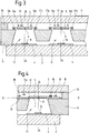
- Figure 1 shows the principle of construction and operation of a network 1 of light shutters according to the invention, in accordance with a first embodiment.
- the shutters 1a, 1b ... each define an optical path X-X which is preferably parallel to the general direction of the incident light L striking the grating. It is clear that the latter includes a large number of shutters 1a, 1b .... etc. cooperating together and arranged, for example, in a matrix.
- the network 1 comprises a transparent plate 2, preferably made of glass, through which enters the light beam L.
- the network comprises an outlet plate 3, also transparent and preferably made of glass, through which leaves the Lm light modulated according to the network control mode (for example matrix).
- Each shutter 1a, 1b, .... comprises, centered on the optical path XX which is associated with it, a converging focusing lens 4, a micro-flap 5 pierced with a diaphragm 6 and having a reflecting surface 7, as well as 'an additional reflecting surface 8 which is formed on the lens 4.
- the shutter 1a is in a so-called non-activated configuration, which means that no control voltage is not applied to it.
- the shutter allows light to pass through its diaphragm 6, the incident light L being first focused by the lens 4, returned backwards by the reflecting surface 7 of the microvalve 5, returned again forwards by the additional reflecting surface 8, and finally sent outwards through the diaphragm 6 to pass through the support plate 3 and become a component of the beam of modulated light Lm.
- the shutter 1b is represented in its so-called activated configuration in which its microvalve 5 is turned by a small angle (7 ° for example) around an axis YY (not indicated in FIG. 1) which is perpendicular to axis XX.
- a control voltage must be applied to the shutter; which will be described in detail later.
- not activated and activated used in the present description should not be taken in the strict sense. Indeed, they simply designate the presence, respectively the absence, of light at the outlet of a shutter, situations which can be obtained, either by the presence or by the absence of a control voltage according to the configuration and the forms electrodes which are associated with each microvolet.
- the network comprises an input plate 2 and an output plate 3. Between these plates 2 and 3 is disposed a plate 9 forming a substrate which is preferably made of silicon. This plate 9 is micro-machined to form microvolets 5 and the sets of electrodes associated therewith.
- a frame 10 forming a spacer surrounds the network of microvolets and maintains a defined distance between the outlet plate 3 and the plate 9.
- the network 1 is matrix with rows Ra, Rb, Rc ... and columns Ca, Cb, Cc ... of shutters resp. Ra-1, Ra-2, Ra-3 ...., Rb-1, Rb-2, Rb-3 ... etc., the rows which can typically include 100 shutters and the number of rows can be 50, for example in the same network.
- FIG. 5 which is a perspective view of a single microvalve 5 and its electrodes, clearly shows that the microvalve 5 is disposed in an opening 11 formed in the plate 9 and that it is attached to the latter by two elastic fasteners (or suspension arms) 12 aligned along the axis YY perpendicular to the optical axis XX of l shutter considered, this axis YY being the axis of rotation of the microvalve 3.
- control 13 and stop 15a and 15b electrodes extend across the opening 11 above each microvalve 5. Furthermore, the conductors 16 cross the conductors 14 and 18 without being electrically connected to them.
- the network designed in this way can be controlled in a matrix fashion by applying to the conductors 14, 16 and 18 appropriate signals in binary form.
- the network makes it possible to transform a wide light beam into a series of light points in a matrix, each point of which can be controlled individually.
- the reflective surfaces 7 and 8 are advantageously produced in the form of aluminum layers deposited by evaporation or spraying techniques.
- the lenses 4 can be formed directly by micromachining in the input plate 2, for example in the form of Fresnel lenses, in the center of which the layers forming the additional reflecting surfaces 8 are respectively provided.
- the lenses can also be produced in the form of diffracting optical elements.
- a microvolet of the network 1 can have a square shape of 100 microns per side, the diaphragm 6 being circular and having a diameter chosen between 5 and 20 microns. Due to the small angle of rotation of the microvolets, the switching time of each shutter can be only 50 microseconds with a control voltage of 15 Volts.
- FIGS. 6 and 7. An example of application of a network 1 according to the invention is shown in FIGS. 6 and 7.
- a network 1 is placed in an opaque capsule 19 in the form of a cylindrical box, the bottom 20 of which is pierced, so that a beam of light can be introduced therein from an optical fiber 21.
- the network 1 is placed in the opening of the capsule 19, a collimating lens 22 being placed in its vicinity to form, from the incoming beam, a collimated beam irradiating the network 1.
- this can include 100 shutters per row and 50 shutters per column.
- Figure 7 shows schematically and in plan how the network 1 and lens 22 can be combined, the bottom 20 of the capsule being assumed to be removed.
- Figure 8 shows an application of a series of capsules 19 according to Figures 6 and 7 to form a light distribution device.
- a light source 23 is connected by a bundle 24 of optical fibers to a row of capsules 19.
- This arrangement allows for example the printing of high definition pages by scrolling through a photosensitive medium in front of the row of capsules, each array of microvolets being suitably ordered as described above.
- a light modulating network according to the invention could provide high definition by providing for each color component a network comprising a very large number of shutters.
- FIG. 9 shows a variant of the invention which can be produced at each shutter in the network.
- a microvolet 5A with its reflecting surface 7A, is placed in the center of the focusing lens 4A, while the additional mirror 8A is provided on the opposite side and provided with the diaphragm 6A.
- FIG. 10 represents another embodiment of the invention which, from an optical point of view, is similar to the embodiment of FIGS. 3 to 5, but which differs therefrom in its construction.
- the network of shutters is produced directly on the outlet plate 3 instead of being in a separate silicon wafer.
- the network is then constructed using thin layers of polysilicon having the same electrodes as in FIGS. 3 to 5. It may be desirable not only in this embodiment, but also in those described above, to provide for supplement a so-called compensation electrode indicated by the reference 25 in FIG. 10.
- the purpose of this electrode is to maintain the microvalve 5 in its horizontal position, when it is in the rest state. Indeed, it can happen that in the absence of any control voltage, the latter is slightly rotated.
Landscapes
- Physics & Mathematics (AREA)
- General Physics & Mathematics (AREA)
- Optics & Photonics (AREA)
- Engineering & Computer Science (AREA)
- Theoretical Computer Science (AREA)
- Mechanical Light Control Or Optical Switches (AREA)
- Micromachines (AREA)
- Use Of Switch Circuits For Exchanges And Methods Of Control Of Multiplex Exchanges (AREA)
Applications Claiming Priority (2)
| Application Number | Priority Date | Filing Date | Title |
|---|---|---|---|
| FR9310960 | 1993-09-13 | ||
| FR9310960A FR2710161B1 (fr) | 1993-09-13 | 1993-09-13 | Réseau miniature d'obturateurs de lumière. |
Publications (2)
| Publication Number | Publication Date |
|---|---|
| EP0643378A1 true EP0643378A1 (de) | 1995-03-15 |
| EP0643378B1 EP0643378B1 (de) | 1997-12-17 |
Family
ID=9450871
Family Applications (1)
| Application Number | Title | Priority Date | Filing Date |
|---|---|---|---|
| EP94114127A Expired - Lifetime EP0643378B1 (de) | 1993-09-13 | 1994-09-08 | Mikronetzlichtverschluss |
Country Status (9)
| Country | Link |
|---|---|
| US (1) | US5579149A (de) |
| EP (1) | EP0643378B1 (de) |
| JP (1) | JP3485206B2 (de) |
| DE (1) | DE69407370T2 (de) |
| DK (1) | DK0643378T3 (de) |
| ES (1) | ES2113019T3 (de) |
| FI (1) | FI114509B (de) |
| FR (1) | FR2710161B1 (de) |
| NO (1) | NO309215B1 (de) |
Families Citing this family (227)
| Publication number | Priority date | Publication date | Assignee | Title |
|---|---|---|---|---|
| US5835255A (en) * | 1986-04-23 | 1998-11-10 | Etalon, Inc. | Visible spectrum modulator arrays |
| US6674562B1 (en) | 1994-05-05 | 2004-01-06 | Iridigm Display Corporation | Interferometric modulation of radiation |
| US7297471B1 (en) | 2003-04-15 | 2007-11-20 | Idc, Llc | Method for manufacturing an array of interferometric modulators |
| US7123216B1 (en) | 1994-05-05 | 2006-10-17 | Idc, Llc | Photonic MEMS and structures |
| US7138984B1 (en) | 2001-06-05 | 2006-11-21 | Idc, Llc | Directly laminated touch sensitive screen |
| US7460291B2 (en) | 1994-05-05 | 2008-12-02 | Idc, Llc | Separable modulator |
| US8014059B2 (en) | 1994-05-05 | 2011-09-06 | Qualcomm Mems Technologies, Inc. | System and method for charge control in a MEMS device |
| US6040937A (en) * | 1994-05-05 | 2000-03-21 | Etalon, Inc. | Interferometric modulation |
| US6710908B2 (en) | 1994-05-05 | 2004-03-23 | Iridigm Display Corporation | Controlling micro-electro-mechanical cavities |
| US20010003487A1 (en) * | 1996-11-05 | 2001-06-14 | Mark W. Miles | Visible spectrum modulator arrays |
| US7550794B2 (en) | 2002-09-20 | 2009-06-23 | Idc, Llc | Micromechanical systems device comprising a displaceable electrode and a charge-trapping layer |
| US6680792B2 (en) | 1994-05-05 | 2004-01-20 | Iridigm Display Corporation | Interferometric modulation of radiation |
| US6046840A (en) | 1995-06-19 | 2000-04-04 | Reflectivity, Inc. | Double substrate reflective spatial light modulator with self-limiting micro-mechanical elements |
| US7907319B2 (en) | 1995-11-06 | 2011-03-15 | Qualcomm Mems Technologies, Inc. | Method and device for modulating light with optical compensation |
| US5916179A (en) * | 1997-04-18 | 1999-06-29 | Sharrock; Nigel | System and method for reducing iatrogenic damage to nerves |
| GB2328312B (en) * | 1997-08-14 | 1999-08-04 | John Quentin Phillipps | Mirror controlled display device |
| US6191882B1 (en) | 1997-09-22 | 2001-02-20 | Creo Srl | Micromachined linear light valve |
| US7532377B2 (en) | 1998-04-08 | 2009-05-12 | Idc, Llc | Movable micro-electromechanical device |
| US8928967B2 (en) | 1998-04-08 | 2015-01-06 | Qualcomm Mems Technologies, Inc. | Method and device for modulating light |
| WO1999052006A2 (en) | 1998-04-08 | 1999-10-14 | Etalon, Inc. | Interferometric modulation of radiation |
| US6529310B1 (en) | 1998-09-24 | 2003-03-04 | Reflectivity, Inc. | Deflectable spatial light modulator having superimposed hinge and deflectable element |
| CN100343717C (zh) * | 1998-09-24 | 2007-10-17 | 反射公司 | 带有自限制微型机械元件的双层介质反射空间光调制器 |
| EP1116063B1 (de) * | 1998-09-24 | 2006-06-07 | Reflectivity Inc. | Reflektierender räumlicher lichtmodulator mit doppelsubstrat und selbstbeschränkenden mikromechanischen elementen |
| US6201633B1 (en) | 1999-06-07 | 2001-03-13 | Xerox Corporation | Micro-electromechanical based bistable color display sheets |
| JP3643508B2 (ja) * | 1999-09-28 | 2005-04-27 | 株式会社東芝 | 可動フィルム型表示装置 |
| WO2003007049A1 (en) | 1999-10-05 | 2003-01-23 | Iridigm Display Corporation | Photonic mems and structures |
| US6396619B1 (en) | 2000-01-28 | 2002-05-28 | Reflectivity, Inc. | Deflectable spatial light modulator having stopping mechanisms |
| US6741383B2 (en) | 2000-08-11 | 2004-05-25 | Reflectivity, Inc. | Deflectable micromirrors with stopping mechanisms |
| US6535318B1 (en) | 1999-11-12 | 2003-03-18 | Jds Uniphase Corporation | Integrated optoelectronic devices having pop-up mirrors therein and methods of forming and operating same |
| WO2001048549A1 (en) * | 1999-12-23 | 2001-07-05 | Alcatel | Shutter for satellite tracking antenna |
| US6325554B1 (en) | 2000-03-15 | 2001-12-04 | Eastman Kodak Company | Camera with electrostatic light valve that functions as image reflecting mirror for viewfinder |
| US6443637B1 (en) | 2000-03-15 | 2002-09-03 | Eastman Kodak Company | Camera with electrostatic light valve that functions as diaphragm |
| JP2002006241A (ja) * | 2000-06-19 | 2002-01-09 | Sony Corp | 光スイッチング素子およびこれを用いたスイッチング装置並びに画像表示装置 |
| US7099065B2 (en) * | 2000-08-03 | 2006-08-29 | Reflectivity, Inc. | Micromirrors with OFF-angle electrodes and stops |
| US6589625B1 (en) | 2001-08-01 | 2003-07-08 | Iridigm Display Corporation | Hermetic seal and method to create the same |
| EP2201965A1 (de) * | 2001-11-08 | 2010-06-30 | Ziscoat N.V. | Intraluminale Vorrichtung mit einer therapeutisches-mittel enthaltenden Beschichtung |
| US6794119B2 (en) | 2002-02-12 | 2004-09-21 | Iridigm Display Corporation | Method for fabricating a structure for a microelectromechanical systems (MEMS) device |
| US6574033B1 (en) | 2002-02-27 | 2003-06-03 | Iridigm Display Corporation | Microelectromechanical systems device and method for fabricating same |
| US7781850B2 (en) | 2002-09-20 | 2010-08-24 | Qualcomm Mems Technologies, Inc. | Controlling electromechanical behavior of structures within a microelectromechanical systems device |
| US7405860B2 (en) * | 2002-11-26 | 2008-07-29 | Texas Instruments Incorporated | Spatial light modulators with light blocking/absorbing areas |
| TWI289708B (en) | 2002-12-25 | 2007-11-11 | Qualcomm Mems Technologies Inc | Optical interference type color display |
| JP2010172190A (ja) * | 2002-12-27 | 2010-08-05 | Nippon Signal Co Ltd:The | プレーナ型電磁アクチュエータ |
| TW200413810A (en) | 2003-01-29 | 2004-08-01 | Prime View Int Co Ltd | Light interference display panel and its manufacturing method |
| TW594360B (en) | 2003-04-21 | 2004-06-21 | Prime View Int Corp Ltd | A method for fabricating an interference display cell |
| TW570896B (en) | 2003-05-26 | 2004-01-11 | Prime View Int Co Ltd | A method for fabricating an interference display cell |
| JP3934578B2 (ja) * | 2003-06-09 | 2007-06-20 | ペンタックス株式会社 | 走査ミラー、ビーム走査型プローブ |
| US7221495B2 (en) | 2003-06-24 | 2007-05-22 | Idc Llc | Thin film precursor stack for MEMS manufacturing |
| TWI231865B (en) | 2003-08-26 | 2005-05-01 | Prime View Int Co Ltd | An interference display cell and fabrication method thereof |
| TW593126B (en) | 2003-09-30 | 2004-06-21 | Prime View Int Co Ltd | A structure of a micro electro mechanical system and manufacturing the same |
| JP2005121906A (ja) * | 2003-10-16 | 2005-05-12 | Fuji Photo Film Co Ltd | 反射型光変調アレイ素子及び露光装置 |
| US7012726B1 (en) | 2003-11-03 | 2006-03-14 | Idc, Llc | MEMS devices with unreleased thin film components |
| US7161728B2 (en) | 2003-12-09 | 2007-01-09 | Idc, Llc | Area array modulation and lead reduction in interferometric modulators |
| US7532194B2 (en) | 2004-02-03 | 2009-05-12 | Idc, Llc | Driver voltage adjuster |
| US7342705B2 (en) | 2004-02-03 | 2008-03-11 | Idc, Llc | Spatial light modulator with integrated optical compensation structure |
| US7119945B2 (en) * | 2004-03-03 | 2006-10-10 | Idc, Llc | Altering temporal response of microelectromechanical elements |
| US7706050B2 (en) | 2004-03-05 | 2010-04-27 | Qualcomm Mems Technologies, Inc. | Integrated modulator illumination |
| US7476327B2 (en) | 2004-05-04 | 2009-01-13 | Idc, Llc | Method of manufacture for microelectromechanical devices |
| US7060895B2 (en) | 2004-05-04 | 2006-06-13 | Idc, Llc | Modifying the electro-mechanical behavior of devices |
| US7164520B2 (en) | 2004-05-12 | 2007-01-16 | Idc, Llc | Packaging for an interferometric modulator |
| US7787170B2 (en) * | 2004-06-15 | 2010-08-31 | Texas Instruments Incorporated | Micromirror array assembly with in-array pillars |
| US7113322B2 (en) * | 2004-06-23 | 2006-09-26 | Reflectivity, Inc | Micromirror having offset addressing electrode |
| US7256922B2 (en) | 2004-07-02 | 2007-08-14 | Idc, Llc | Interferometric modulators with thin film transistors |
| KR101313117B1 (ko) | 2004-07-29 | 2013-09-30 | 퀄컴 엠이엠에스 테크놀로지스, 인크. | 간섭 변조기의 미소기전 동작을 위한 시스템 및 방법 |
| US7420725B2 (en) | 2004-09-27 | 2008-09-02 | Idc, Llc | Device having a conductive light absorbing mask and method for fabricating same |
| US7405861B2 (en) | 2004-09-27 | 2008-07-29 | Idc, Llc | Method and device for protecting interferometric modulators from electrostatic discharge |
| US7460246B2 (en) | 2004-09-27 | 2008-12-02 | Idc, Llc | Method and system for sensing light using interferometric elements |
| US7317568B2 (en) | 2004-09-27 | 2008-01-08 | Idc, Llc | System and method of implementation of interferometric modulators for display mirrors |
| US8124434B2 (en) | 2004-09-27 | 2012-02-28 | Qualcomm Mems Technologies, Inc. | Method and system for packaging a display |
| US7553684B2 (en) | 2004-09-27 | 2009-06-30 | Idc, Llc | Method of fabricating interferometric devices using lift-off processing techniques |
| US7343080B2 (en) | 2004-09-27 | 2008-03-11 | Idc, Llc | System and method of testing humidity in a sealed MEMS device |
| US7289256B2 (en) | 2004-09-27 | 2007-10-30 | Idc, Llc | Electrical characterization of interferometric modulators |
| US7304784B2 (en) | 2004-09-27 | 2007-12-04 | Idc, Llc | Reflective display device having viewable display on both sides |
| US7813026B2 (en) | 2004-09-27 | 2010-10-12 | Qualcomm Mems Technologies, Inc. | System and method of reducing color shift in a display |
| US7920135B2 (en) | 2004-09-27 | 2011-04-05 | Qualcomm Mems Technologies, Inc. | Method and system for driving a bi-stable display |
| US7369294B2 (en) | 2004-09-27 | 2008-05-06 | Idc, Llc | Ornamental display device |
| US7561323B2 (en) | 2004-09-27 | 2009-07-14 | Idc, Llc | Optical films for directing light towards active areas of displays |
| US7373026B2 (en) | 2004-09-27 | 2008-05-13 | Idc, Llc | MEMS device fabricated on a pre-patterned substrate |
| US7583429B2 (en) | 2004-09-27 | 2009-09-01 | Idc, Llc | Ornamental display device |
| US7349136B2 (en) | 2004-09-27 | 2008-03-25 | Idc, Llc | Method and device for a display having transparent components integrated therein |
| US7259449B2 (en) | 2004-09-27 | 2007-08-21 | Idc, Llc | Method and system for sealing a substrate |
| US7327510B2 (en) | 2004-09-27 | 2008-02-05 | Idc, Llc | Process for modifying offset voltage characteristics of an interferometric modulator |
| US7936497B2 (en) | 2004-09-27 | 2011-05-03 | Qualcomm Mems Technologies, Inc. | MEMS device having deformable membrane characterized by mechanical persistence |
| US7130104B2 (en) | 2004-09-27 | 2006-10-31 | Idc, Llc | Methods and devices for inhibiting tilting of a mirror in an interferometric modulator |
| US7692839B2 (en) | 2004-09-27 | 2010-04-06 | Qualcomm Mems Technologies, Inc. | System and method of providing MEMS device with anti-stiction coating |
| US8008736B2 (en) | 2004-09-27 | 2011-08-30 | Qualcomm Mems Technologies, Inc. | Analog interferometric modulator device |
| US20060076634A1 (en) | 2004-09-27 | 2006-04-13 | Lauren Palmateer | Method and system for packaging MEMS devices with incorporated getter |
| US7372613B2 (en) | 2004-09-27 | 2008-05-13 | Idc, Llc | Method and device for multistate interferometric light modulation |
| US7417783B2 (en) | 2004-09-27 | 2008-08-26 | Idc, Llc | Mirror and mirror layer for optical modulator and method |
| US7355780B2 (en) | 2004-09-27 | 2008-04-08 | Idc, Llc | System and method of illuminating interferometric modulators using backlighting |
| US7349141B2 (en) | 2004-09-27 | 2008-03-25 | Idc, Llc | Method and post structures for interferometric modulation |
| US7359066B2 (en) | 2004-09-27 | 2008-04-15 | Idc, Llc | Electro-optical measurement of hysteresis in interferometric modulators |
| US7719500B2 (en) | 2004-09-27 | 2010-05-18 | Qualcomm Mems Technologies, Inc. | Reflective display pixels arranged in non-rectangular arrays |
| US7916103B2 (en) | 2004-09-27 | 2011-03-29 | Qualcomm Mems Technologies, Inc. | System and method for display device with end-of-life phenomena |
| US7710629B2 (en) | 2004-09-27 | 2010-05-04 | Qualcomm Mems Technologies, Inc. | System and method for display device with reinforcing substance |
| US7424198B2 (en) | 2004-09-27 | 2008-09-09 | Idc, Llc | Method and device for packaging a substrate |
| US7453579B2 (en) | 2004-09-27 | 2008-11-18 | Idc, Llc | Measurement of the dynamic characteristics of interferometric modulators |
| US7527995B2 (en) | 2004-09-27 | 2009-05-05 | Qualcomm Mems Technologies, Inc. | Method of making prestructure for MEMS systems |
| US7564612B2 (en) | 2004-09-27 | 2009-07-21 | Idc, Llc | Photonic MEMS and structures |
| US7630119B2 (en) | 2004-09-27 | 2009-12-08 | Qualcomm Mems Technologies, Inc. | Apparatus and method for reducing slippage between structures in an interferometric modulator |
| US7653371B2 (en) | 2004-09-27 | 2010-01-26 | Qualcomm Mems Technologies, Inc. | Selectable capacitance circuit |
| US7429334B2 (en) | 2004-09-27 | 2008-09-30 | Idc, Llc | Methods of fabricating interferometric modulators by selectively removing a material |
| US7893919B2 (en) | 2004-09-27 | 2011-02-22 | Qualcomm Mems Technologies, Inc. | Display region architectures |
| US7535466B2 (en) | 2004-09-27 | 2009-05-19 | Idc, Llc | System with server based control of client device display features |
| US7415186B2 (en) | 2004-09-27 | 2008-08-19 | Idc, Llc | Methods for visually inspecting interferometric modulators for defects |
| US20060176487A1 (en) | 2004-09-27 | 2006-08-10 | William Cummings | Process control monitors for interferometric modulators |
| US7492502B2 (en) | 2004-09-27 | 2009-02-17 | Idc, Llc | Method of fabricating a free-standing microstructure |
| US7701631B2 (en) | 2004-09-27 | 2010-04-20 | Qualcomm Mems Technologies, Inc. | Device having patterned spacers for backplates and method of making the same |
| US7299681B2 (en) | 2004-09-27 | 2007-11-27 | Idc, Llc | Method and system for detecting leak in electronic devices |
| US7554714B2 (en) | 2004-09-27 | 2009-06-30 | Idc, Llc | Device and method for manipulation of thermal response in a modulator |
| US7161730B2 (en) | 2004-09-27 | 2007-01-09 | Idc, Llc | System and method for providing thermal compensation for an interferometric modulator display |
| US7321456B2 (en) | 2004-09-27 | 2008-01-22 | Idc, Llc | Method and device for corner interferometric modulation |
| US7944599B2 (en) | 2004-09-27 | 2011-05-17 | Qualcomm Mems Technologies, Inc. | Electromechanical device with optical function separated from mechanical and electrical function |
| US7684104B2 (en) | 2004-09-27 | 2010-03-23 | Idc, Llc | MEMS using filler material and method |
| US7586484B2 (en) | 2004-09-27 | 2009-09-08 | Idc, Llc | Controller and driver features for bi-stable display |
| US7368803B2 (en) | 2004-09-27 | 2008-05-06 | Idc, Llc | System and method for protecting microelectromechanical systems array using back-plate with non-flat portion |
| US7668415B2 (en) | 2004-09-27 | 2010-02-23 | Qualcomm Mems Technologies, Inc. | Method and device for providing electronic circuitry on a backplate |
| US7369296B2 (en) | 2004-09-27 | 2008-05-06 | Idc, Llc | Device and method for modifying actuation voltage thresholds of a deformable membrane in an interferometric modulator |
| US7405924B2 (en) | 2004-09-27 | 2008-07-29 | Idc, Llc | System and method for protecting microelectromechanical systems array using structurally reinforced back-plate |
| US7808703B2 (en) | 2004-09-27 | 2010-10-05 | Qualcomm Mems Technologies, Inc. | System and method for implementation of interferometric modulator displays |
| US7302157B2 (en) | 2004-09-27 | 2007-11-27 | Idc, Llc | System and method for multi-level brightness in interferometric modulation |
| US7417735B2 (en) | 2004-09-27 | 2008-08-26 | Idc, Llc | Systems and methods for measuring color and contrast in specular reflective devices |
| US7750886B2 (en) | 2004-09-27 | 2010-07-06 | Qualcomm Mems Technologies, Inc. | Methods and devices for lighting displays |
| US7289259B2 (en) | 2004-09-27 | 2007-10-30 | Idc, Llc | Conductive bus structure for interferometric modulator array |
| US20060083768A1 (en) * | 2004-09-28 | 2006-04-20 | Atrium Medical Corporation | Method of thickening a coating using a drug |
| WO2006037049A2 (en) * | 2004-09-28 | 2006-04-06 | Atrium Medical Corporation | Application of a coating on a medical device |
| WO2007011385A2 (en) | 2004-09-28 | 2007-01-25 | Atrium Medical Corporation | Heat cured gel and method of making |
| US9592324B2 (en) | 2006-11-06 | 2017-03-14 | Atrium Medical Corporation | Tissue separating device with reinforced support for anchoring mechanisms |
| US8312836B2 (en) | 2004-09-28 | 2012-11-20 | Atrium Medical Corporation | Method and apparatus for application of a fresh coating on a medical device |
| US8367099B2 (en) | 2004-09-28 | 2013-02-05 | Atrium Medical Corporation | Perforated fatty acid films |
| US9000040B2 (en) | 2004-09-28 | 2015-04-07 | Atrium Medical Corporation | Cross-linked fatty acid-based biomaterials |
| US9012506B2 (en) | 2004-09-28 | 2015-04-21 | Atrium Medical Corporation | Cross-linked fatty acid-based biomaterials |
| US9801982B2 (en) | 2004-09-28 | 2017-10-31 | Atrium Medical Corporation | Implantable barrier device |
| US8124127B2 (en) | 2005-10-15 | 2012-02-28 | Atrium Medical Corporation | Hydrophobic cross-linked gels for bioabsorbable drug carrier coatings |
| US7092143B2 (en) * | 2004-10-19 | 2006-08-15 | Reflectivity, Inc | Micromirror array device and a method for making the same |
| TW200628877A (en) | 2005-02-04 | 2006-08-16 | Prime View Int Co Ltd | Method of manufacturing optical interference type color display |
| US7295363B2 (en) | 2005-04-08 | 2007-11-13 | Texas Instruments Incorporated | Optical coating on light transmissive substrates of micromirror devices |
| GB0510470D0 (en) * | 2005-05-23 | 2005-06-29 | Qinetiq Ltd | Coded aperture imaging system |
| WO2007013939A1 (en) | 2005-07-22 | 2007-02-01 | Qualcomm Incorporated | Support structure for mems device and methods therefor |
| US9278161B2 (en) | 2005-09-28 | 2016-03-08 | Atrium Medical Corporation | Tissue-separating fatty acid adhesion barrier |
| US9427423B2 (en) | 2009-03-10 | 2016-08-30 | Atrium Medical Corporation | Fatty-acid based particles |
| US7630114B2 (en) | 2005-10-28 | 2009-12-08 | Idc, Llc | Diffusion barrier layer for MEMS devices |
| US7795061B2 (en) | 2005-12-29 | 2010-09-14 | Qualcomm Mems Technologies, Inc. | Method of creating MEMS device cavities by a non-etching process |
| US7636151B2 (en) | 2006-01-06 | 2009-12-22 | Qualcomm Mems Technologies, Inc. | System and method for providing residual stress test structures |
| US7916980B2 (en) | 2006-01-13 | 2011-03-29 | Qualcomm Mems Technologies, Inc. | Interconnect structure for MEMS device |
| US7382515B2 (en) | 2006-01-18 | 2008-06-03 | Qualcomm Mems Technologies, Inc. | Silicon-rich silicon nitrides as etch stops in MEMS manufacture |
| GB2434935A (en) * | 2006-02-06 | 2007-08-08 | Qinetiq Ltd | Coded aperture imager using reference object to form decoding pattern |
| GB2434934A (en) * | 2006-02-06 | 2007-08-08 | Qinetiq Ltd | Processing coded aperture image data by applying weightings to aperture functions and data frames |
| GB0602380D0 (en) * | 2006-02-06 | 2006-03-15 | Qinetiq Ltd | Imaging system |
| GB2434877A (en) * | 2006-02-06 | 2007-08-08 | Qinetiq Ltd | MOEMS optical modulator |
| GB2434937A (en) | 2006-02-06 | 2007-08-08 | Qinetiq Ltd | Coded aperture imaging apparatus performing image enhancement |
| GB2434936A (en) | 2006-02-06 | 2007-08-08 | Qinetiq Ltd | Imaging system having plural distinct coded aperture arrays at different mask locations |
| US7603001B2 (en) | 2006-02-17 | 2009-10-13 | Qualcomm Mems Technologies, Inc. | Method and apparatus for providing back-lighting in an interferometric modulator display device |
| US7582952B2 (en) | 2006-02-21 | 2009-09-01 | Qualcomm Mems Technologies, Inc. | Method for providing and removing discharging interconnect for chip-on-glass output leads and structures thereof |
| US7547568B2 (en) | 2006-02-22 | 2009-06-16 | Qualcomm Mems Technologies, Inc. | Electrical conditioning of MEMS device and insulating layer thereof |
| US7550810B2 (en) | 2006-02-23 | 2009-06-23 | Qualcomm Mems Technologies, Inc. | MEMS device having a layer movable at asymmetric rates |
| US7450295B2 (en) | 2006-03-02 | 2008-11-11 | Qualcomm Mems Technologies, Inc. | Methods for producing MEMS with protective coatings using multi-component sacrificial layers |
| US7643203B2 (en) | 2006-04-10 | 2010-01-05 | Qualcomm Mems Technologies, Inc. | Interferometric optical display system with broadband characteristics |
| US7903047B2 (en) | 2006-04-17 | 2011-03-08 | Qualcomm Mems Technologies, Inc. | Mode indicator for interferometric modulator displays |
| US7527996B2 (en) | 2006-04-19 | 2009-05-05 | Qualcomm Mems Technologies, Inc. | Non-planar surface structures and process for microelectromechanical systems |
| US7623287B2 (en) | 2006-04-19 | 2009-11-24 | Qualcomm Mems Technologies, Inc. | Non-planar surface structures and process for microelectromechanical systems |
| US7711239B2 (en) | 2006-04-19 | 2010-05-04 | Qualcomm Mems Technologies, Inc. | Microelectromechanical device and method utilizing nanoparticles |
| US7417784B2 (en) | 2006-04-19 | 2008-08-26 | Qualcomm Mems Technologies, Inc. | Microelectromechanical device and method utilizing a porous surface |
| US7369292B2 (en) | 2006-05-03 | 2008-05-06 | Qualcomm Mems Technologies, Inc. | Electrode and interconnect materials for MEMS devices |
| US7321457B2 (en) | 2006-06-01 | 2008-01-22 | Qualcomm Incorporated | Process and structure for fabrication of MEMS device having isolated edge posts |
| US7649671B2 (en) | 2006-06-01 | 2010-01-19 | Qualcomm Mems Technologies, Inc. | Analog interferometric modulator device with electrostatic actuation and release |
| US7405863B2 (en) | 2006-06-01 | 2008-07-29 | Qualcomm Mems Technologies, Inc. | Patterning of mechanical layer in MEMS to reduce stresses at supports |
| US7471442B2 (en) | 2006-06-15 | 2008-12-30 | Qualcomm Mems Technologies, Inc. | Method and apparatus for low range bit depth enhancements for MEMS display architectures |
| US7766498B2 (en) | 2006-06-21 | 2010-08-03 | Qualcomm Mems Technologies, Inc. | Linear solid state illuminator |
| US7385744B2 (en) | 2006-06-28 | 2008-06-10 | Qualcomm Mems Technologies, Inc. | Support structure for free-standing MEMS device and methods for forming the same |
| US7835061B2 (en) | 2006-06-28 | 2010-11-16 | Qualcomm Mems Technologies, Inc. | Support structures for free-standing electromechanical devices |
| US7388704B2 (en) | 2006-06-30 | 2008-06-17 | Qualcomm Mems Technologies, Inc. | Determination of interferometric modulator mirror curvature and airgap variation using digital photographs |
| US7527998B2 (en) | 2006-06-30 | 2009-05-05 | Qualcomm Mems Technologies, Inc. | Method of manufacturing MEMS devices providing air gap control |
| GB0615040D0 (en) * | 2006-07-28 | 2006-09-06 | Qinetiq Ltd | Processing method for coded apperture sensor |
| US7566664B2 (en) | 2006-08-02 | 2009-07-28 | Qualcomm Mems Technologies, Inc. | Selective etching of MEMS using gaseous halides and reactive co-etchants |
| US7763546B2 (en) | 2006-08-02 | 2010-07-27 | Qualcomm Mems Technologies, Inc. | Methods for reducing surface charges during the manufacture of microelectromechanical systems devices |
| EP1943551A2 (de) | 2006-10-06 | 2008-07-16 | Qualcomm Mems Technologies, Inc. | Lichtführung |
| CN103558686B (zh) | 2006-10-06 | 2017-03-01 | 追踪有限公司 | 集成于显示器的照明设备中的光学损失结构 |
| US9492596B2 (en) | 2006-11-06 | 2016-11-15 | Atrium Medical Corporation | Barrier layer with underlying medical device and one or more reinforcing support structures |
| US7719752B2 (en) | 2007-05-11 | 2010-05-18 | Qualcomm Mems Technologies, Inc. | MEMS structures, methods of fabricating MEMS components on separate substrates and assembly of same |
| US7949213B2 (en) | 2007-12-07 | 2011-05-24 | Qualcomm Mems Technologies, Inc. | Light illumination of displays with front light guide and coupling elements |
| US8068710B2 (en) | 2007-12-07 | 2011-11-29 | Qualcomm Mems Technologies, Inc. | Decoupled holographic film and diffuser |
| WO2009129264A1 (en) | 2008-04-15 | 2009-10-22 | Qualcomm Mems Technologies, Inc. | Light with bi-directional propagation |
| DE102008019600B4 (de) * | 2008-04-18 | 2021-03-04 | Fraunhofer-Gesellschaft zur Förderung der angewandten Forschung e.V. | Optische Vorrichtung in gestapelter Bauweise und Verfahren zur Herstellung derselben |
| GB0822281D0 (en) * | 2008-12-06 | 2009-01-14 | Qinetiq Ltd | Optically diverse coded aperture imaging |
| US8172417B2 (en) | 2009-03-06 | 2012-05-08 | Qualcomm Mems Technologies, Inc. | Shaped frontlight reflector for use with display |
| US8979349B2 (en) | 2009-05-29 | 2015-03-17 | Qualcomm Mems Technologies, Inc. | Illumination devices and methods of fabrication thereof |
| US20110038910A1 (en) | 2009-08-11 | 2011-02-17 | Atrium Medical Corporation | Anti-infective antimicrobial-containing biomaterials |
| US11592723B2 (en) | 2009-12-22 | 2023-02-28 | View, Inc. | Automated commissioning of controllers in a window network |
| US10303035B2 (en) | 2009-12-22 | 2019-05-28 | View, Inc. | Self-contained EC IGU |
| US20210063836A1 (en) | 2017-04-26 | 2021-03-04 | View, Inc. | Building network |
| US10747082B2 (en) | 2009-12-22 | 2020-08-18 | View, Inc. | Onboard controller for multistate windows |
| US8213074B1 (en) | 2011-03-16 | 2012-07-03 | Soladigm, Inc. | Onboard controller for multistate windows |
| JP2013524287A (ja) | 2010-04-09 | 2013-06-17 | クォルコム・メムズ・テクノロジーズ・インコーポレーテッド | 電気機械デバイスの機械層及びその形成方法 |
| EP2593141B1 (de) | 2010-07-16 | 2018-07-04 | Atrium Medical Corporation | Zusammensetzung und verfahren zur veränderung der geschwindigkeit einer hydrolyse ausgehärteter materialien auf ölbasis |
| US8705162B2 (en) | 2012-04-17 | 2014-04-22 | View, Inc. | Controlling transitions in optically switchable devices |
| US11415949B2 (en) | 2011-03-16 | 2022-08-16 | View, Inc. | Security event detection with smart windows |
| US11822202B2 (en) | 2011-03-16 | 2023-11-21 | View, Inc. | Controlling transitions in optically switchable devices |
| US11703814B2 (en) | 2011-03-16 | 2023-07-18 | View, Inc. | Security event detection with smart windows |
| US10989977B2 (en) | 2011-03-16 | 2021-04-27 | View, Inc. | Onboard controller for multistate windows |
| US11054792B2 (en) | 2012-04-13 | 2021-07-06 | View, Inc. | Monitoring sites containing switchable optical devices and controllers |
| US9134527B2 (en) | 2011-04-04 | 2015-09-15 | Qualcomm Mems Technologies, Inc. | Pixel via and methods of forming the same |
| US8963159B2 (en) | 2011-04-04 | 2015-02-24 | Qualcomm Mems Technologies, Inc. | Pixel via and methods of forming the same |
| JP5803615B2 (ja) * | 2011-11-29 | 2015-11-04 | 富士通株式会社 | 電子デバイスとその製造方法 |
| EP3223532B1 (de) | 2012-04-13 | 2019-10-09 | View, Inc. | Anwendungen zur steuerung optisch schaltbarer vorrichtungen |
| US10964320B2 (en) | 2012-04-13 | 2021-03-30 | View, Inc. | Controlling optically-switchable devices |
| US12400651B2 (en) | 2012-04-13 | 2025-08-26 | View Operating Corporation | Controlling optically-switchable devices |
| US11255120B2 (en) | 2012-05-25 | 2022-02-22 | View, Inc. | Tester and electrical connectors for insulated glass units |
| US9867880B2 (en) | 2012-06-13 | 2018-01-16 | Atrium Medical Corporation | Cured oil-hydrogel biomaterial compositions for controlled drug delivery |
| US11150616B2 (en) | 2014-03-05 | 2021-10-19 | View, Inc. | Site monitoring system |
| US11868103B2 (en) | 2014-03-05 | 2024-01-09 | View, Inc. | Site monitoring system |
| KR102336168B1 (ko) | 2014-03-05 | 2021-12-07 | 뷰, 인크. | 스위칭가능한 광 디바이스들 및 제어기들을 포함하는 사이트들 모니터링 |
| US10481459B2 (en) | 2014-06-30 | 2019-11-19 | View, Inc. | Control methods and systems for networks of optically switchable windows during reduced power availability |
| US11003041B2 (en) | 2014-06-30 | 2021-05-11 | View, Inc. | Power management for electrochromic window networks |
| US11740948B2 (en) | 2014-12-08 | 2023-08-29 | View, Inc. | Multiple interacting systems at a site |
| CA2970300A1 (en) | 2014-12-08 | 2016-06-16 | View, Inc. | Multiple interacting systems at a site |
| DE102015112296A1 (de) * | 2015-07-28 | 2017-02-02 | Valeo Schalter Und Sensoren Gmbh | Optische Sensorvorrichtung für ein Kraftfahrzeug, Kraftfahrzeug sowie Verfahren |
| US12366111B2 (en) | 2015-09-18 | 2025-07-22 | View Operating Corporation | Trunk line window controllers |
| US11384596B2 (en) | 2015-09-18 | 2022-07-12 | View, Inc. | Trunk line window controllers |
| CA3039342A1 (en) | 2016-10-03 | 2018-04-12 | View, Inc. | Site monitoring system |
| US12603091B2 (en) | 2017-04-26 | 2026-04-14 | View Operating Corporation | Immersive collaboration of remote participants via media displays |
| TW201907213A (zh) | 2017-04-26 | 2019-02-16 | 美商唯景公司 | 可著色窗系統計算平台 |
| US11747696B2 (en) | 2017-04-26 | 2023-09-05 | View, Inc. | Tandem vision window and media display |
| US12147142B2 (en) | 2017-04-26 | 2024-11-19 | View, Inc. | Remote management of a facility |
| US10571683B2 (en) * | 2017-11-28 | 2020-02-25 | Aptiv Technologies Limited | Multi-faceted MEMS mirror device useful for vehicle LIDAR |
| JP7644501B2 (ja) | 2019-05-09 | 2025-03-12 | ビュー オペレーティング コーポレーション | 建物内の制御されたカバレッジのためのアンテナシステム |
| US11631493B2 (en) | 2020-05-27 | 2023-04-18 | View Operating Corporation | Systems and methods for managing building wellness |
| TW202206925A (zh) | 2020-03-26 | 2022-02-16 | 美商視野公司 | 多用戶端網路中之存取及傳訊 |
Citations (6)
| Publication number | Priority date | Publication date | Assignee | Title |
|---|---|---|---|---|
| US4383255A (en) * | 1980-03-11 | 1983-05-10 | Centre Electronique Horloger S.A. | Miniature display device |
| FR2542105A1 (fr) * | 1983-03-04 | 1984-09-07 | Canon Kk | Element de modulation optique et son procede de commande |
| EP0143079A2 (de) * | 1983-11-18 | 1985-05-29 | Centre Electronique Horloger S.A. | Herstellungsverfahren für eine Mikroklappenvorrichtung und Anwendung dieses Verfahrens zur Schaffung eines Lichtmodulators |
| US4566935A (en) * | 1984-07-31 | 1986-01-28 | Texas Instruments Incorporated | Spatial light modulator and method |
| EP0453400A1 (de) * | 1990-04-20 | 1991-10-23 | Centre Suisse D'electronique Et De Microtechnique S.A. | Matrixadressierte Lichtmodulationsvorrichtung |
| EP0469293A1 (de) * | 1990-06-29 | 1992-02-05 | Texas Instruments Incorporated | Mehrschichtige verformbare Spiegelstruktur |
Family Cites Families (7)
| Publication number | Priority date | Publication date | Assignee | Title |
|---|---|---|---|---|
| US4087810A (en) * | 1976-06-30 | 1978-05-02 | International Business Machines Corporation | Membrane deformographic display, and method of making |
| US4420896A (en) * | 1981-09-17 | 1983-12-20 | General Electric Company | Method for fabrication of electroscopic display devices and transmissive display devices fabricated thereby |
| US4571603A (en) * | 1981-11-03 | 1986-02-18 | Texas Instruments Incorporated | Deformable mirror electrostatic printer |
| EP0246547A3 (de) * | 1986-05-22 | 1990-06-13 | Siemens Aktiengesellschaft | Anordnung zur optischen Bildverarbeitung |
| DE3741856C1 (de) * | 1987-12-10 | 1989-04-20 | Messerschmitt Boelkow Blohm | Optronische stoergeschuetzte Flugkoerperortung |
| US5101236A (en) * | 1989-12-21 | 1992-03-31 | Texas Instruments Incorporated | Light energy control system and method of operation |
| GB9107144D0 (en) * | 1991-04-05 | 1991-05-22 | Rank Cintel Ltd | Recording video signals on cinematographic film |
-
1993
- 1993-09-13 FR FR9310960A patent/FR2710161B1/fr not_active Expired - Fee Related
-
1994
- 1994-09-08 DK DK94114127T patent/DK0643378T3/da active
- 1994-09-08 DE DE69407370T patent/DE69407370T2/de not_active Expired - Lifetime
- 1994-09-08 ES ES94114127T patent/ES2113019T3/es not_active Expired - Lifetime
- 1994-09-08 EP EP94114127A patent/EP0643378B1/de not_active Expired - Lifetime
- 1994-09-12 FI FI944198A patent/FI114509B/fi not_active IP Right Cessation
- 1994-09-12 US US08/304,689 patent/US5579149A/en not_active Expired - Lifetime
- 1994-09-12 NO NO943381A patent/NO309215B1/no not_active IP Right Cessation
- 1994-09-13 JP JP24344494A patent/JP3485206B2/ja not_active Expired - Lifetime
Patent Citations (6)
| Publication number | Priority date | Publication date | Assignee | Title |
|---|---|---|---|---|
| US4383255A (en) * | 1980-03-11 | 1983-05-10 | Centre Electronique Horloger S.A. | Miniature display device |
| FR2542105A1 (fr) * | 1983-03-04 | 1984-09-07 | Canon Kk | Element de modulation optique et son procede de commande |
| EP0143079A2 (de) * | 1983-11-18 | 1985-05-29 | Centre Electronique Horloger S.A. | Herstellungsverfahren für eine Mikroklappenvorrichtung und Anwendung dieses Verfahrens zur Schaffung eines Lichtmodulators |
| US4566935A (en) * | 1984-07-31 | 1986-01-28 | Texas Instruments Incorporated | Spatial light modulator and method |
| EP0453400A1 (de) * | 1990-04-20 | 1991-10-23 | Centre Suisse D'electronique Et De Microtechnique S.A. | Matrixadressierte Lichtmodulationsvorrichtung |
| EP0469293A1 (de) * | 1990-06-29 | 1992-02-05 | Texas Instruments Incorporated | Mehrschichtige verformbare Spiegelstruktur |
Non-Patent Citations (4)
| Title |
|---|
| K.E.PETERSEN: "micromecanical light deflector array", IBM TECNICAL DISCLOSURE BULLETIN, vol. 20, no. 1, June 1977 (1977-06-01), US, pages 355 - 356 * |
| L.J.HORNBECK: "deformable mirror spatial light modulators", SPATIAL LIGHT MODULATORS AND APPLICATIONS, August 1989 (1989-08-01), SAN DIEGO CA US, pages 86 - 102, XP000351394 * |
| R.VUILLEUMIER: "novel electromechanical microshutter display device", EURODISPLAY, September 1984 (1984-09-01), PARIS FRANCE, pages 441 - 44 * |
| V.P.JAECKLIN: "optical microshutter and torsional micromirrors for nlight modulator arrays", MEMS, 10 February 1993 (1993-02-10), FT. LAUDERDALE EUA, pages 124 - 127 * |
Also Published As
| Publication number | Publication date |
|---|---|
| FI944198A7 (fi) | 1995-03-14 |
| JPH07181404A (ja) | 1995-07-21 |
| EP0643378B1 (de) | 1997-12-17 |
| US5579149A (en) | 1996-11-26 |
| NO943381D0 (no) | 1994-09-12 |
| JP3485206B2 (ja) | 2004-01-13 |
| FR2710161B1 (fr) | 1995-11-24 |
| FI114509B (fi) | 2004-10-29 |
| NO309215B1 (no) | 2000-12-27 |
| FI944198A0 (fi) | 1994-09-12 |
| DK0643378T3 (da) | 1998-08-24 |
| FR2710161A1 (fr) | 1995-03-24 |
| DE69407370T2 (de) | 1998-07-09 |
| NO943381L (no) | 1995-03-14 |
| ES2113019T3 (es) | 1998-04-16 |
| DE69407370D1 (de) | 1998-01-29 |
Similar Documents
| Publication | Publication Date | Title |
|---|---|---|
| EP0643378B1 (de) | Mikronetzlichtverschluss | |
| US7116463B2 (en) | High angular deflection micro-mirror system | |
| US6337760B1 (en) | Encapsulated multi-directional light beam steering device | |
| EP0802439B1 (de) | Optomechanische Mikrovorrichtung und ihre optomechanischen Anwendung in einem Mikro-Strahlablenker | |
| US6046840A (en) | Double substrate reflective spatial light modulator with self-limiting micro-mechanical elements | |
| EP0475796B1 (de) | Bildprojektionssystem mit Verwendung von zwei orthogonalen Lichtpolarizationskomponenten | |
| EP0633702B1 (de) | Farbanzeigegerät | |
| EP1116063B1 (de) | Reflektierender räumlicher lichtmodulator mit doppelsubstrat und selbstbeschränkenden mikromechanischen elementen | |
| FR2664712A1 (fr) | Dispositif de modulation optique a cellules deformables. | |
| US7095545B2 (en) | Microelectromechanical device with reset electrode | |
| EP0880724A1 (de) | Anzeigevorrichtung und flacher fernsehbildschirm, der diese vorrichtung benutzt | |
| WO2009121810A1 (fr) | Lunettes informatives | |
| FR2737595A1 (fr) | Dispositif d'affichage a cristaux liquides | |
| EP1637914B1 (de) | Lokal deformierbarer Spiegel aus elektroaktivem Material, dessen Dicke mittels elektrischen Effekten variiert werden kann | |
| EP0881527A1 (de) | Räumliches optisches Schaltsystem mit akustooptischem Mehrkanal-Ablenker | |
| EP1410092B1 (de) | Optisches ablenkmodul | |
| JP2001183591A (ja) | マイクロミラー光学スイッチ | |
| FR2706666A1 (fr) | Panneau d'affichage à cristaux liquides et projecteur à cristaux liquides utilisant ce dernier. | |
| EP0645020A1 (de) | Rundumsichtgerät mit optimaler raumabdeckung durch aneinanderfügen von sichtfeldern | |
| EP0611454A1 (de) | Vorrichtung für Mikroabtastung und Infrarotkamera ausgestattet mit einer solchen Vorrichtung | |
| JP4718740B2 (ja) | 光アドドロップマルチプレクサ | |
| EP4038447B1 (de) | Thermooptisch adressierter räumlicher lichtmodulator | |
| EP4075182A1 (de) | Optischer scanner | |
| EP1243902B1 (de) | Spektrophotometer mit electrostatischen Mikroverschlüssen | |
| EP3983837B1 (de) | Optische matrixarraykomponente zum fokussieren eines einfallenden lichtstrahls auf eine reihe von punkten |
Legal Events
| Date | Code | Title | Description |
|---|---|---|---|
| PUAI | Public reference made under article 153(3) epc to a published international application that has entered the european phase |
Free format text: ORIGINAL CODE: 0009012 |
|
| AK | Designated contracting states |
Kind code of ref document: A1 Designated state(s): BE CH DE DK ES FR GB IT LI NL |
|
| 17P | Request for examination filed |
Effective date: 19950817 |
|
| 17Q | First examination report despatched |
Effective date: 19960812 |
|
| GRAG | Despatch of communication of intention to grant |
Free format text: ORIGINAL CODE: EPIDOS AGRA |
|
| GRAH | Despatch of communication of intention to grant a patent |
Free format text: ORIGINAL CODE: EPIDOS IGRA |
|
| GRAH | Despatch of communication of intention to grant a patent |
Free format text: ORIGINAL CODE: EPIDOS IGRA |
|
| GRAA | (expected) grant |
Free format text: ORIGINAL CODE: 0009210 |
|
| AK | Designated contracting states |
Kind code of ref document: B1 Designated state(s): BE CH DE DK ES FR GB IT LI NL |
|
| REG | Reference to a national code |
Ref country code: CH Ref legal event code: EP |
|
| REF | Corresponds to: |
Ref document number: 69407370 Country of ref document: DE Date of ref document: 19980129 |
|
| ITF | It: translation for a ep patent filed | ||
| REG | Reference to a national code |
Ref country code: CH Ref legal event code: NV Representative=s name: ICB INGENIEURS CONSEILS EN BREVETS SA |
|
| GBT | Gb: translation of ep patent filed (gb section 77(6)(a)/1977) |
Effective date: 19980313 |
|
| REG | Reference to a national code |
Ref country code: ES Ref legal event code: FG2A Ref document number: 2113019 Country of ref document: ES Kind code of ref document: T3 |
|
| REG | Reference to a national code |
Ref country code: DK Ref legal event code: T3 |
|
| PLBE | No opposition filed within time limit |
Free format text: ORIGINAL CODE: 0009261 |
|
| STAA | Information on the status of an ep patent application or granted ep patent |
Free format text: STATUS: NO OPPOSITION FILED WITHIN TIME LIMIT |
|
| 26N | No opposition filed | ||
| REG | Reference to a national code |
Ref country code: CH Ref legal event code: PUE Owner name: CSEM, CENTRE SUISSE D'ELECTRONIQUE ET DE MICROTECH Ref country code: CH Ref legal event code: NV Representative=s name: CSEM CENTRE SUISSE D'ELECTRONIQUE ET DE MICROTECHN |
|
| REG | Reference to a national code |
Ref country code: GB Ref legal event code: IF02 |
|
| REG | Reference to a national code |
Ref country code: GB Ref legal event code: 732E |
|
| REG | Reference to a national code |
Ref country code: FR Ref legal event code: TP |
|
| REG | Reference to a national code |
Ref country code: ES Ref legal event code: PC2A |
|
| NLS | Nl: assignments of ep-patents |
Owner name: COLIBRYS S.A. |
|
| REG | Reference to a national code |
Ref country code: CH Ref legal event code: NV Representative=s name: CABINET ROLAND NITHARDT CONSEILS EN PROPRIETE INDU |
|
| REG | Reference to a national code |
Ref country code: CH Ref legal event code: PCAR Free format text: PATENTS & TECHNOLOGY SURVEYS SA;RUE DES TERREAUX 7 CASE POSTALE 2848;2001 NEUCHATEL (CH) |
|
| REG | Reference to a national code |
Ref country code: CH Ref legal event code: PFA Owner name: COLIBRYS SA Free format text: COLIBRYS SA#MALADIERE 83#2007 NEUCHATEL (CH) -TRANSFER TO- COLIBRYS SA#MALADIERE 83#2007 NEUCHATEL (CH) |
|
| PGFP | Annual fee paid to national office [announced via postgrant information from national office to epo] |
Ref country code: NL Payment date: 20130918 Year of fee payment: 20 Ref country code: ES Payment date: 20130927 Year of fee payment: 20 Ref country code: DK Payment date: 20130918 Year of fee payment: 20 Ref country code: DE Payment date: 20130919 Year of fee payment: 20 Ref country code: CH Payment date: 20130919 Year of fee payment: 20 |
|
| PGFP | Annual fee paid to national office [announced via postgrant information from national office to epo] |
Ref country code: GB Payment date: 20130919 Year of fee payment: 20 Ref country code: FR Payment date: 20130919 Year of fee payment: 20 |
|
| PGFP | Annual fee paid to national office [announced via postgrant information from national office to epo] |
Ref country code: BE Payment date: 20130919 Year of fee payment: 20 |
|
| PGFP | Annual fee paid to national office [announced via postgrant information from national office to epo] |
Ref country code: IT Payment date: 20130930 Year of fee payment: 20 |
|
| REG | Reference to a national code |
Ref country code: DE Ref legal event code: R071 Ref document number: 69407370 Country of ref document: DE |
|
| REG | Reference to a national code |
Ref country code: CH Ref legal event code: PL Ref country code: DK Ref legal event code: EUP Effective date: 20140908 |
|
| REG | Reference to a national code |
Ref country code: NL Ref legal event code: V4 Effective date: 20140908 |
|
| REG | Reference to a national code |
Ref country code: GB Ref legal event code: PE20 Expiry date: 20140907 |
|
| PG25 | Lapsed in a contracting state [announced via postgrant information from national office to epo] |
Ref country code: DE Free format text: LAPSE BECAUSE OF EXPIRATION OF PROTECTION Effective date: 20140909 |
|
| PG25 | Lapsed in a contracting state [announced via postgrant information from national office to epo] |
Ref country code: GB Free format text: LAPSE BECAUSE OF EXPIRATION OF PROTECTION Effective date: 20140907 |
|
| REG | Reference to a national code |
Ref country code: ES Ref legal event code: FD2A Effective date: 20150108 |
|
| PG25 | Lapsed in a contracting state [announced via postgrant information from national office to epo] |
Ref country code: ES Free format text: LAPSE BECAUSE OF EXPIRATION OF PROTECTION Effective date: 20140909 |