EP0643420A2 - Procédé de lift-off pour des transistors à couches minces auto-alignés - Google Patents
Procédé de lift-off pour des transistors à couches minces auto-alignés Download PDFInfo
- Publication number
- EP0643420A2 EP0643420A2 EP94306358A EP94306358A EP0643420A2 EP 0643420 A2 EP0643420 A2 EP 0643420A2 EP 94306358 A EP94306358 A EP 94306358A EP 94306358 A EP94306358 A EP 94306358A EP 0643420 A2 EP0643420 A2 EP 0643420A2
- Authority
- EP
- European Patent Office
- Prior art keywords
- layer
- upper cap
- source
- intermediate body
- cap layer
- Prior art date
- Legal status (The legal status is an assumption and is not a legal conclusion. Google has not performed a legal analysis and makes no representation as to the accuracy of the status listed.)
- Granted
Links
Images

Classifications
-
- H—ELECTRICITY
- H10—SEMICONDUCTOR DEVICES; ELECTRIC SOLID-STATE DEVICES NOT OTHERWISE PROVIDED FOR
- H10D—INORGANIC ELECTRIC SEMICONDUCTOR DEVICES
- H10D30/00—Field-effect transistors [FET]
- H10D30/01—Manufacture or treatment
- H10D30/021—Manufacture or treatment of FETs having insulated gates [IGFET]
- H10D30/031—Manufacture or treatment of FETs having insulated gates [IGFET] of thin-film transistors [TFT]
- H10D30/0321—Manufacture or treatment of FETs having insulated gates [IGFET] of thin-film transistors [TFT] comprising silicon, e.g. amorphous silicon or polysilicon
-
- H—ELECTRICITY
- H10—SEMICONDUCTOR DEVICES; ELECTRIC SOLID-STATE DEVICES NOT OTHERWISE PROVIDED FOR
- H10D—INORGANIC ELECTRIC SEMICONDUCTOR DEVICES
- H10D30/00—Field-effect transistors [FET]
- H10D30/01—Manufacture or treatment
- H10D30/021—Manufacture or treatment of FETs having insulated gates [IGFET]
- H10D30/031—Manufacture or treatment of FETs having insulated gates [IGFET] of thin-film transistors [TFT]
- H10D30/0312—Manufacture or treatment of FETs having insulated gates [IGFET] of thin-film transistors [TFT] characterised by the gate electrodes
- H10D30/0316—Manufacture or treatment of FETs having insulated gates [IGFET] of thin-film transistors [TFT] characterised by the gate electrodes of lateral bottom-gate TFTs comprising only a single gate
-
- H—ELECTRICITY
- H10—SEMICONDUCTOR DEVICES; ELECTRIC SOLID-STATE DEVICES NOT OTHERWISE PROVIDED FOR
- H10D—INORGANIC ELECTRIC SEMICONDUCTOR DEVICES
- H10D30/00—Field-effect transistors [FET]
- H10D30/60—Insulated-gate field-effect transistors [IGFET]
- H10D30/67—Thin-film transistors [TFT]
- H10D30/674—Thin-film transistors [TFT] characterised by the active materials
-
- H—ELECTRICITY
- H10—SEMICONDUCTOR DEVICES; ELECTRIC SOLID-STATE DEVICES NOT OTHERWISE PROVIDED FOR
- H10D—INORGANIC ELECTRIC SEMICONDUCTOR DEVICES
- H10D30/00—Field-effect transistors [FET]
- H10D30/60—Insulated-gate field-effect transistors [IGFET]
- H10D30/67—Thin-film transistors [TFT]
- H10D30/6757—Thin-film transistors [TFT] characterised by the structure of the channel, e.g. transverse or longitudinal shape or doping profile
-
- Y—GENERAL TAGGING OF NEW TECHNOLOGICAL DEVELOPMENTS; GENERAL TAGGING OF CROSS-SECTIONAL TECHNOLOGIES SPANNING OVER SEVERAL SECTIONS OF THE IPC; TECHNICAL SUBJECTS COVERED BY FORMER USPC CROSS-REFERENCE ART COLLECTIONS [XRACs] AND DIGESTS
- Y10—TECHNICAL SUBJECTS COVERED BY FORMER USPC
- Y10S—TECHNICAL SUBJECTS COVERED BY FORMER USPC CROSS-REFERENCE ART COLLECTIONS [XRACs] AND DIGESTS
- Y10S148/00—Metal treatment
- Y10S148/10—Lift-off masking
Definitions
- This invention is related to Copending Application PCT/US 94/01737 EP 94909684.6 (corresponding to the US application of G.Possin et al entitled “Self-Aligned Thin-Film Transistor Constructed Using Lift-Off Technique", Serial No. 08/024,050, filed 1 March 1993), and the European application 94302246.7 (corresponoding to the US application of R.Kwasnick et al entitled “Self-Aligned Thin Film Transistor Constructed Using Lift-Off Technique", Serial No. 08/043,043, filed 5 April 1993) both of which are assigned to the assignee of the present invention and are incorporated herein by reference.
- This invention relates to the manufacture of thin-film field effect transistors, and in particular to a method of patterning the source and drain electrodes to have a desired alignment with the gate electrode.
- TFTs thin film field effect transistors
- imaging and display devices a TFT is commonly associated with each pixel to enable a respective electrical signal to be coupled to or from each individual pixel.
- the TFT be as small as possible.
- the large number of pixels in an array require that the associated TFTs be relatively small so as to not require physically larger arrays.
- array performance is improved as TFT size is decreased because total gate capacitance, gate to source capacitance, and gate to drain capacitance can be minimized.
- the total gate capacitance should be small in order to reduce the total capacitance of the address line (e.g., a scan line) that control a row of TFTs in the imaging or display device.
- the charging time of the address line is controlled by the product of the line resistance and line capacitance.
- the total gate capacitance is added to the line capacitance in determining the address line charging time.
- the gate to drain and gate to source capacitances, respectively, should be small to minimize the coupling capacitance between the input address line, which is connected to the gate, and imaging or display element connected to the source or drain.
- a primary determinant of the gate to source and gate to drain capacitances is the overlap of the source and drain electrodes, respectively, over the gate electrode. Fabrication of small TFTs with the source and drain electrodes aligned over the gate electrode can be difficult. One reason is that photolithographic processes are commonly used to pattern the source and the drain electrode, and there is typically some positioning misalignment of about 2 microns or more that must be accounted for in device layout. This amount of misalignment requires that the regions where the gate overlaps the source and drain be made larger than otherwise required. These enlarged sizes to account for the misalignment result in increased gate to source and gate to drain capacitances as noted above.
- One object of the present invention is to provide an improved fabrication process for TFTs having self-aligned source and drain electrodes
- Another object of the present invention is to provide a self-aligned lift-off method of fabricating a TFT that provides faster lift-off times.
- a method of fabricating a self-aligned thin film transistor (TFT) using a lift-off technique includes the steps of forming a multi-tiered island on a layer of semiconductor material overlying a gate electrode such that a base portion of the multi-tiered island has dimensions corresponding to the desired overlap of the source and drain electrodes, forming source and drain electrodes having the desired overlap over the gate electrode, and removing all but the base portion of the multi-tier island.
- the multi-tiered island includes an inorganic dielectric material base layer, an organic dielectric material intermediate body layer, and a transparent conducting oxide upper cap layer, with the upper cap layer having a lip that overhangs the intermediate body layer by about 0.5 ⁇ m and 1.5 ⁇ m.
- the source and drain electrode material is deposited over the semiconductor material and the multi-tier island such that the electrode material is disposed over the semiconductor material and abuts the base layer of the multi-tier island; a portion of the underside of lip of the upper cap layer remains substantially free of the source and drain electrode material.
- the assembly is exposed to an etchant that is selective to the source-drain electrode material and such that the etchant is exposed to the underside of the lip of the upper cap layer to allow the upper cap layer to be etched away in a lift-off technique.
- the upper cap layer typically comprises indium tin oxide and the intermediate body layer typically comprises polyimide, and hydrochloric acid (HCl) is used as an etchant to effect the lift-off of the upper cap layer in a process that is accelerated as result of the hydrolization effect of the HCl at the polyimide/indium tin oxide interface.
- HCl hydrochloric acid
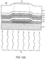
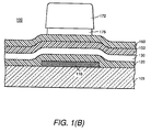
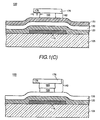
- Figures 1(A)-1(D) are a simplified representation of part of the sequence of steps used in constructing a TFT in accordance with the invention.
- Figures 2(A)-2(B) are a simplified representation of the lift-off portion of the procedure of the present invention.
- TFTs thin film transistors
- FIG 1(A) illustrates a point in the fabrication process showing a TFT assembly 100 in which a gate electrode 110 has been formed on a substrate 105, such as can be accomplished using known techniques.
- TFT assembly refers generally to the structure of the materials deposited and patterned to form the TFT at any point of the fabrication process.
- Substrate 105 typically comprises glass (such as Corning 7059 glass) or the like that is substantially transparent to light of wavelength in the ultraviolet range (e.g., 400 nm), which is used as described below for patterning portions of the device using a through the substrate exposure technique.
- Gate electrode 110 typically comprises a metal such as chromium, aluminum, tungsten, or the like, and alternatively may comprise one or more layers of a conductive material.
- the gate electrode typically has a thickness in a range of about 0.1 ⁇ m to 0.5 ⁇ m.
- a gate dielectric layer 120 is deposited over substrate 105 and gate electrode 110.
- Gate dielectric layer typically comprises silicon nitride, silicon oxide or the like has a thickness in the range between about 50-500 nm.
- a semiconductor material layer 130 is deposited over gate dielectric layer, and typically comprises an amorphous semiconductor material such as amorphous silicon or the like having a thickness in the range between about 20 nm to 100 nm thick.
- a multi-tier island 140 is formed on semiconductor layer 130 over gate electrode 110.
- An inorganic dielectric layer 150 ( Figure 1(A)) comprising a substantially optically transparent material such as silicon nitride, or alternatively silicon oxide or similar PECVD-deposited dielectrics or the like, is deposited over semiconductor material layer 130 and has a thickness between about 100 nm and 1000 nm. It is generally desirable that inorganic dielectric layer 150 be thinner (within the range given above) if it will later be etched in a wet etch process (as described more fully below).
- gate dielectric layer 120, semiconductor material layer 130, and inorganic dielectric layer 150 are deposited by plasma enhanced chemical vapor deposition (PECVD) in a single vacuum pumpdown.
- PECVD plasma enhanced chemical vapor deposition
- An organic dielectric layer 160 is deposited over inorganic dielectric material layer 150, and typically comprises polyimide (PI).
- the layer of Pl film is typically spun on TFT assembly 100, and then annealed at temperatures up to about 250 °C.
- the PI film typically has a thickness between about 200 nm to 1200 nm, and is substantially transparent to light having a wavelength in the ultraviolet range (e.g., 400 nm), which is used as described below for patterning portions of the device using a through the substrate exposure technique.
- a wavelength in the ultraviolet range e.g. 400 nm
- One example of PI film having acceptable light transmission characteristics is Ciba-Geigy 293 polyimide; a layer having a thickness of about 500 nm has a transmission of about 80% for light in the 400 nm wavelength range
- a transparent conducting oxide layer 170 that is substantially light transmissive at the frequency of light used in the backside exposure technique is deposited over organic dielectric layer 160, such as by sputtering.
- Layer 170 typically comprises indium tin oxide (ITO) that has a thickness in the range between about 100 nm to 200 nm.
- ITO indium tin oxide
- An alternative transparent conducting oxide material that can be deposited is zinc oxide (ZnO).
- An ITO layer having a thickness between about 100 nm and 200 nm exhibits about 80% transmission of light having a wavelength about 400 nm.
- Transparent conducting oxide layer 170 is next patterned with a through-the-substrate (or backside) exposure technique to form upper cap layer 175 of multi-tier island 140 ( Figure 1(D)).
- a photoresist layer 172 is deposited over ITO layer 170 and assembly 100 is then exposed to light 75, typically ultraviolet light having a wavelength of about 400 nm, from a source on the side of substrate 105 opposite gate electrode 110, as illustrated in Figure 1(A).
- the exposure time of the photoresist using light sources of comparable intensity, must be longer for the backside exposure technique than with the conventional front side exposure to account for attenuation of the light in the layers of TFT assembly 100.
- the increase in exposure time for the TFT assembly of the present invention is somewhat longer than that required in the process of U.S. Patent 5,010,027, for example, because of the presence of organic dielectric layer 160 and ITO layer 170, which collectively increase the exposure time by a factor of about 50% over that required for a TFT assembly without layers 160 and 170.
- gate 110 casts a shadow 76 on photoresist layer 172 within the region bounded by the dashed lines in Figure 1(A).
- the exposed photoresist that is, the area outside of the shadow
- ITO layer 170 is etched to remove the portion of the ITO not underlying the photoresist mask.
- the ITO is typically etched in a reactive ion etching process or alternatively in a wet etching process using, for example, oxalic acid.
- the etchant must be selective to organic dielectric layer 160; it should be noted that certain common wet etchants, such as hydrochloric acid, are not appropriate for use in this step as the HCl will degrade the underlying polyimide layer 160. Particularly in a wet etching process, some undercutting of ITO layer is common, but as long as such undercutting does not exceed 0.5 ⁇ m, it does not adversely affect the self-alignment process. TFT assembly 100 appears as illustrated in Figure 1(B) at the conclusion of etching ITO layer 170.
- Remaining portions of photoresist layer 172 can then be stripped using a photoresist stripper (such as Ciba-Geigy photoresist stripper QZ3298, which does not attack the exposed PI material in layer 160).
- a photoresist stripper such as Ciba-Geigy photoresist stripper QZ3298, which does not attack the exposed PI material in layer 160.
- the residual photoresist can be stripped at a later point in the TFT fabrication process, such as prior to etching inorganic dielectric layer 150.
- the remaining portion of ITO layer comprises upper cap 175 of multi-tier island 140 ( Figures 1(C) and 1 (D)).
- Polyimide layer 160 is next etched using the patterned ITO layer 170 (that is, upper cap 175) as a mask.
- the etch process is an oxygen plasma etch, which is conducted for a selected time so as etch the PI from the exposed regions of TFT assembly 100 and further to create an undercut profile under upper cap 175.
- the etch is timed to provide an undercut region 162 (detailed in Figure 1(C), but not necessarily with correct proportions).
- Undercut region 162 in which the PI has been etched away from underneath the ITO forms a lip 176 in upper cap layer 175.
- the amount of the undercut, or length "L" of the lip 176 is between about 0.5 ⁇ m and 1.5 ⁇ m.
- the remaining, or patterned, portions of PI layer 160 comprise intermediate body layer 165 of multi-tier island 140 ( Figures 1(C) and 1(D)).
- Inorganic dielectric layer 150 is next etched, using the overlying layers of PI and ITO as a mask.
- silicon nitride which typically comprises the inorganic dielectric material in layer 150, is etched in a wet etch process using hydrofluoric acid (HF) or buffered HF (BHF) using intermediate body layer 165 as a mask to remove the exposed portions of the silicon nitride.
- HF hydrofluoric acid
- BHF buffered HF
- ITO upper cap layer 175 acts as the primary mask to define the boundary (or sidewall) of the portion of silicon nitride layer 150 remaining after this etching step, which comprises base layer 155 of multi-tier island 140.
- the island structure illustrated in Figure 1(D) illustrates a structure that would typically result from the use of the wet etch process, in which the dimensions of silicon nitride base layer 155 is defined primarily by the patterned PI forming the intermediate body layer 165 (some undercutting of base layer 155 may occur, but typically is quite minimal, e.g., less than about 0.5 ⁇ m).
- base portion is substantially centered over gate electrode 110 and has a lateral dimension corresponding to overlying layers of multi-tier island 140.
- multi-tier island 140 has been formed and appears as illustrated in Figure 1(D).
- the lateral dimension (i.e., in the plane of the paper of the Figures) of upper cap layer 175 is determined by the backside exposure technique; the lateral dimension intermediate body layer 165 is determined by the length of upper cap layer 175 and the timed etching of the PI to achieve an undercut of upper cap layer 175 with the desired dimensions (e.g., about 0.5 ⁇ m to 1.5 ⁇ m undercut); and the lateral dimension of base layer 155 is substantially the same as that of intermediate body layer 165.
- the lateral dimension of base layer 155 is thus determined by the backside exposure self-alignment technique.
- TFT assembly 100 is next prepared for the formation of the source and drain electrodes by cleaning the exposed surfaces in a brief (e.g., about 30 seconds) wet etch in diluted BHF (e.g., a 1% solution of the standard commercially-available HF solution).
- diluted BHF e.g., a 1% solution of the standard commercially-available HF solution
- source and drain electrodes are formed by the deposition over TFT assembly 100 of appropriate source-drain material to form the electrodes.
- a layer of doped semiconductive material 180 e.g., silicon doped to exhibit n+ conductivity, is first deposited over TFT assembly 100.
- the doped semiconductive material comprises n+ amorphous silicon (n+ Si) or, alternatively, n+ microcrystalline silicon (n+ ⁇ c-Si).
- the doped semiconductive material is deposited in a PECVD process and has a thickness in the range between about 10 nm and 100 nm.
- the doped semiconductive material covers the exposed regions amorphous silicon layer 130 and abuts the sidewalls of base layer 165 of multi-tier island 140; the deposition process further results in an accumulation of doped semiconductive material on the upper surface upper cap layer 175 and which, to some degree, may also wrap around the corner of lip 176; the doped semiconductive material tends to break at the edge of upper cap lip 176 so that substantially none of the material adheres to the underside surface of lip 176.
- substantially none of the material adhering to the underside surface refers to little (e.g., 20 ⁇ ) or no accumulation of the deposited material on the underside such that in the lift-off process, as described below, the etchant applied to remove upper cap layer 175 readily penetrates any deposited material and gains access to the ITO/PI interface.
- the distance D of undercut under lip 176 is selected (e.g., through the timing of the PI etch) to ensure that the source-drain material deposition process substantially does in particular does not cover the corner at the interface between the ITO material of upper cap 175 and the PI of intermediate body layer 165.
- a relatively thin (e.g., 10 nm - 50 nm) metallic conductive material layer 190 is then deposited, usually in a sputtering of evaporation process, over doped semiconductive material layer 180.
- substantially none of the conductive material layer adheres to the underside of lip 176 of upper cap layer 175.
- TFT assembly 100 appears as illustrated in Figure 2(A).
- the thickness of the metallic conductive layer is selected to reduce the combined lateral resistance of the doped semiconductive layer and the metallic conductive layer in the contact region of the TFT (that is, the region above gate electrode 110) so that it is small enough to provide good TFT performance.
- the doped semiconductive material and conductive material deposited over the amorphous silicon semiconductive layer 130 up to the sidewall of base layer 155 comprise the source electrode, and the doped semiconductive and conductive material deposited over the amorphous silicon semiconductive material 130 up to the opposite sidewall of base layer 155 comprises the drain electrode; the determination of which portion comprises the source electrode and which comprises the drain electrode is determined by the connections made to the respective electrodes and is not critical for the purposes of describing this invention.
- the lateral dimension of base portion 155 coupled with its substantially centered placement over gate electrode 110 (as determined by the backside exposure technique and the subsequent etching of ITO layer 170 and PI layer 160) determines the amount overlap of each the source and the drain electrodes over the gate electrode (and hence determines the respective gate to source and gate to drain capacitances).
- Upper cap layer 175 (and the doped semiconductive material and metallic conductive material adhering thereto from the source/drain material deposition processes) is then removed from TFT assembly 100 with a lift-off technique by exposing the assembly to an etchant selective to the source/drain material.
- "Lift-off” refers to an etchant process in which the upper cap layer is detached from the underlying intermediate portion layer (and is removed from the TFT assembly in the etching process) prior to the upper cap layer structure being otherwise destroyed by the etchant, thus saving time by effecting the removal of the structure in less time than is required to etch away the material deposited on and forming upper cap layer 175.
- TFT assembly 100 is wet etched using hydrochloric acid (HCl), which not only etches ITO exposed at the underside of lip 176 of upper cap 175 but also hydrolizes the PI of intermediate body layer 165.
- HCl hydrochloric acid
- This hydrolization of the PI results in a very rapid etch back of the ITO at the ITO-PI interface of upper cap layer 175 and intermediate body layer 165.
- the hydrolization of the PI degrades the structural integrity of the ITO/PI interface, providing faster access of the etchant to the ITO along the length of the interface, such that the etching covers several hundred microns in only a few minutes, resulting in a relatively quick "lifting off" of upper cap layer 175 from intermediate body layer 165.
- the breakdown of the structural integrity of the PI/ITO interface also enables the upper cap layer to be lifted-off sooner than would be possible if the ITO was being removed solely in the etching interactions.
- the etchant applied to lift-off upper cap layer 175 is selective to the source/drain material applied so that the the material comprising the source and drain electrodes is not removed from TFT assembly 100.
- the metallic conductive material layer 190 preferably comprises molybdenum (Mo), as it does not etch in HCl.
- tungsten (W), nickel-chromium (NiCr), tantalum (Ta), and aluminum (Al) can be used to form metallic conductive layer 190, as these materials provide good electrical contact to the n+ doped silicon without damaging the electrical junction between the n+Si and the underlying amorphous silicon while providing sufficiently low lateral resistance for the source and drain electrodes.
- Intermediate body layer 165 is then removed from TFT assembly 100 to complete the fabrication of the TFT.
- the PI intermediate body layer is removed by, for example, etching assembly 100 in an oxygen plasma, which leaves the base layer 155 and the self-aligned source and drain electrodes.
- the array of which TFT assembly 100 is a part is then completed in accordance with known procedures, such as by patterning the source drain material to form the desired address lines and contacts to active areas of the pixel, and the excess n+ Si and amorphous silicon is removed in regions not covered by the source drain material.
- metallic conductive layer 190 comprises chromium (Cr), which is known to react with n+ Si to form a chromium-silicide, following an annealing step at about 200 °C, between the n+ Si and the Cr layer.
- Etching TFT assembly 100 in a solution of HCl after the deposition of the Cr layer serves to etch the Cr in addition to the ITO, and thus any portion of the ITO covered by the Cr, particularly at the ITO/PI interface, is more quickly exposed to the HCl etchant.
- removing the Cr can lessen the overall etch time to effect the lift-off of upper cap layer 175.
- the remaining n+ Si with overlying silicide layer typically provides sufficiently low source/drain electrode lateral resistance for TFT operation.
- a further embodiment of the present invention obviates the need for the deposition of metallic conductive layer 190.
- doped semiconductive layer 180 comprise microcrystalline n+ silicon, which will provide sufficiently low source/drain electrode lateral resistance for TFT operation.
- This method in which no separate metallic conductive layer 190 is deposited provides the opportunity for shorter etch times as the HCl etchant applied to effect the lift-off, as described above, can more quickly breach any thin covering of the n+ material to gain access to the ITO/PI interface portion of the TFT assembly.
- conductive metal access electrodes are typically fabricated to connect the source and drain electrodes in a TFT assembly to an address line or active pixel area, respectively, outside of the gate region.
- alignment is not critical (as it is with determining source and drain electrode placement in the channel region) and these metal contacts can be fabricated using conventional photolithographic techniques.
Landscapes
- Thin Film Transistor (AREA)
Applications Claiming Priority (2)
| Application Number | Priority Date | Filing Date | Title |
|---|---|---|---|
| US115973 | 1980-01-28 | ||
| US08/115,973 US5391507A (en) | 1993-09-03 | 1993-09-03 | Lift-off fabrication method for self-aligned thin film transistors |
Publications (3)
| Publication Number | Publication Date |
|---|---|
| EP0643420A2 true EP0643420A2 (fr) | 1995-03-15 |
| EP0643420A3 EP0643420A3 (fr) | 1997-04-02 |
| EP0643420B1 EP0643420B1 (fr) | 2004-08-18 |
Family
ID=22364477
Family Applications (1)
| Application Number | Title | Priority Date | Filing Date |
|---|---|---|---|
| EP94306358A Expired - Lifetime EP0643420B1 (fr) | 1993-09-03 | 1994-08-30 | Procédé de lift-off pour des transistors à couches minces auto-alignés |
Country Status (4)
| Country | Link |
|---|---|
| US (1) | US5391507A (fr) |
| EP (1) | EP0643420B1 (fr) |
| JP (1) | JP3510681B2 (fr) |
| DE (1) | DE69433948T2 (fr) |
Cited By (1)
| Publication number | Priority date | Publication date | Assignee | Title |
|---|---|---|---|---|
| US10335322B2 (en) | 2013-08-26 | 2019-07-02 | Lightside Md, Llc | Adhesive support devices and methods of making and using them |
Families Citing this family (24)
| Publication number | Priority date | Publication date | Assignee | Title |
|---|---|---|---|---|
| US5399884A (en) * | 1993-11-10 | 1995-03-21 | General Electric Company | Radiation imager with single passivation dielectric for transistor and diode |
| DE4432294A1 (de) * | 1994-09-12 | 1996-03-14 | Telefunken Microelectron | Verfahren zur Reduzierung der Oberflächenrekombinationsgeschwindigkeit in Silizium |
| US5557534A (en) * | 1995-01-03 | 1996-09-17 | Xerox Corporation | Forming array with metal scan lines to control semiconductor gate lines |
| JP3448838B2 (ja) | 1995-06-30 | 2003-09-22 | 富士通株式会社 | 磁気抵抗効果型ヘッドの製造方法 |
| KR0171984B1 (ko) * | 1995-12-11 | 1999-03-30 | 김주용 | 박막 트랜지스터의 자기 정렬 노광 방법 |
| US5717223A (en) * | 1995-12-22 | 1998-02-10 | Xerox Corporation | Array with amorphous silicon TFTs in which channel leads overlap insulating region no more than maximum overlap |
| US5733804A (en) * | 1995-12-22 | 1998-03-31 | Xerox Corporation | Fabricating fully self-aligned amorphous silicon device |
| EP0894148A4 (fr) * | 1996-04-17 | 1999-06-16 | Motorola Inc | Detecteur moleculaire transistorise et procede correspondant |
| US5602047A (en) * | 1996-06-13 | 1997-02-11 | Industrial Technology Research Institute | Process for polysilicon thin film transistors using backside irradiation and plasma doping |
| JPH1050607A (ja) * | 1996-07-31 | 1998-02-20 | Sony Corp | 半導体装置の製造方法 |
| US6403407B1 (en) * | 2000-06-02 | 2002-06-11 | International Business Machines Corporation | Method of forming fully self-aligned TFT with improved process window |
| KR100500779B1 (ko) * | 2003-10-10 | 2005-07-12 | 엘지.필립스 엘시디 주식회사 | 박막 트랜지스터 어레이 기판의 제조 방법 |
| TW200602774A (en) * | 2004-07-06 | 2006-01-16 | Chunghwa Picture Tubes Ltd | Thin-film transistor manufacture method |
| US20070269750A1 (en) * | 2006-05-19 | 2007-11-22 | Eastman Kodak Company | Colored masking for forming transparent structures |
| US8906490B2 (en) * | 2006-05-19 | 2014-12-09 | Eastman Kodak Company | Multicolor mask |
| US8756659B2 (en) * | 2007-04-19 | 2014-06-17 | At&T Intellectual Property I, L.P. | Access authorization servers, methods and computer program products employing wireless terminal location |
| US8129098B2 (en) * | 2007-11-20 | 2012-03-06 | Eastman Kodak Company | Colored mask combined with selective area deposition |
| US8153352B2 (en) * | 2007-11-20 | 2012-04-10 | Eastman Kodak Company | Multicolored mask process for making display circuitry |
| US8221964B2 (en) * | 2007-11-20 | 2012-07-17 | Eastman Kodak Company | Integrated color mask |
| US8173355B2 (en) * | 2007-11-20 | 2012-05-08 | Eastman Kodak Company | Gradient colored mask |
| US9484546B2 (en) | 2013-05-15 | 2016-11-01 | Universal Display Corporation | OLED with compact contact design and self-aligned insulators |
| US10786652B2 (en) | 2013-10-18 | 2020-09-29 | Lightside Md, Llc | Support devices and methods of making and using them |
| CN105655257A (zh) * | 2016-01-13 | 2016-06-08 | 深圳市华星光电技术有限公司 | 薄膜晶体管结构的制造方法 |
| CN108335985B (zh) * | 2017-01-20 | 2020-07-28 | 中国科学院物理研究所 | 一种全透明薄膜晶体管的制备方法 |
Family Cites Families (9)
| Publication number | Priority date | Publication date | Assignee | Title |
|---|---|---|---|---|
| JPS60182134A (ja) * | 1984-02-28 | 1985-09-17 | Fujitsu Ltd | パタ−ン形成方法 |
| DE3640174A1 (de) * | 1985-11-27 | 1987-06-04 | Sharp Kk | Duennfilm-transistor-anordnung |
| JPS62260369A (ja) * | 1986-05-07 | 1987-11-12 | Matsushita Electric Ind Co Ltd | 薄膜トランジスタの製造方法 |
| EP0270323B1 (fr) * | 1986-11-29 | 1999-11-03 | Sharp Kabushiki Kaisha | Méthode de fabrication d'un transistor en couche mince |
| US5254488A (en) * | 1988-01-04 | 1993-10-19 | International Business Machines Corporation | Easily manufacturable thin film transistor structures |
| JPH02288237A (ja) * | 1989-04-27 | 1990-11-28 | Fujitsu Ltd | 薄膜トランジスタの製造方法 |
| US5010027A (en) * | 1990-03-21 | 1991-04-23 | General Electric Company | Method for fabricating a self-aligned thin-film transistor utilizing planarization and back-side photoresist exposure |
| US5153142A (en) * | 1990-09-04 | 1992-10-06 | Industrial Technology Research Institute | Method for fabricating an indium tin oxide electrode for a thin film transistor |
| US5281546A (en) * | 1992-09-02 | 1994-01-25 | General Electric Company | Method of fabricating a thin film transistor using hydrogen plasma treatment of the intrinsic silicon/doped layer interface |
-
1993
- 1993-09-03 US US08/115,973 patent/US5391507A/en not_active Expired - Lifetime
-
1994
- 1994-08-30 EP EP94306358A patent/EP0643420B1/fr not_active Expired - Lifetime
- 1994-08-30 DE DE69433948T patent/DE69433948T2/de not_active Expired - Fee Related
- 1994-09-01 JP JP20829394A patent/JP3510681B2/ja not_active Expired - Fee Related
Cited By (1)
| Publication number | Priority date | Publication date | Assignee | Title |
|---|---|---|---|---|
| US10335322B2 (en) | 2013-08-26 | 2019-07-02 | Lightside Md, Llc | Adhesive support devices and methods of making and using them |
Also Published As
| Publication number | Publication date |
|---|---|
| EP0643420B1 (fr) | 2004-08-18 |
| DE69433948D1 (de) | 2004-09-23 |
| EP0643420A3 (fr) | 1997-04-02 |
| DE69433948T2 (de) | 2005-09-08 |
| JP3510681B2 (ja) | 2004-03-29 |
| US5391507A (en) | 1995-02-21 |
| JPH07153957A (ja) | 1995-06-16 |
Similar Documents
| Publication | Publication Date | Title |
|---|---|---|
| EP0643420B1 (fr) | Procédé de lift-off pour des transistors à couches minces auto-alignés | |
| US4958205A (en) | Thin film transistor array and method of manufacturing the same | |
| US5156986A (en) | Positive control of the source/drain-gate overlap in self-aligned TFTS via a top hat gate electrode configuration | |
| US6362028B1 (en) | Method for fabricating TFT array and devices formed | |
| KR100225098B1 (ko) | 박막트랜지스터의 제조방법 | |
| EP0304657B1 (fr) | Cellule matricielle active et son procédé de fabrication | |
| EP1086490B1 (fr) | Procédé de fabrication de transistors en couches minces | |
| US5751020A (en) | Structure of a liquid crystal display unit having exposed channel region | |
| WO1992006490A1 (fr) | Auto-alignement d'un composant par la propagation d'une topographie de structure de reference | |
| US20020109796A1 (en) | Metal contact structure and method for thin film transistor array in liquid crystal display | |
| US5166086A (en) | Thin film transistor array and method of manufacturing same | |
| US6100950A (en) | Active matrix LCD with thin film transistor switches and method of producing the same | |
| US6875645B2 (en) | Pixel structure and fabricating method thereof | |
| EP0646953B1 (fr) | Méthode pour la réduction du courant de fuite dans des transistors à couche mince | |
| US20040063254A1 (en) | Thin film transistor substrate and method of manufacturing the same | |
| US5541128A (en) | Self-aligned thin-film transistor constructed using lift-off technique | |
| US5527726A (en) | Self-aligned thin-film transistor constructed using lift-off technique | |
| KR0171980B1 (ko) | 액정 표시 소자의 제조방법 | |
| WO1992006497A1 (fr) | Reglage du chevauchement entre l'electrode de grille et les electrodes de source/drain dans un transistor a couches minces auto-aligne via une configuration d'electrode de porte a languette d'ajustement | |
| EP0520713A2 (fr) | Procédé de fabrication d'un transistor en couches minces utilisant un nombre limité d'étapes de masquage | |
| US5523187A (en) | Method for the fabrication of liquid crystal display device | |
| KR950001160B1 (ko) | 박막트랜지스터 및 그의 제조방법 | |
| KR100218578B1 (ko) | 액정표시장치의 구조와 그 제조방법 | |
| JP3097229B2 (ja) | 薄膜トランジスタ素子アレイとその製造方法 | |
| KR100300862B1 (ko) | 박막트랜지스터제조방법 |
Legal Events
| Date | Code | Title | Description |
|---|---|---|---|
| PUAI | Public reference made under article 153(3) epc to a published international application that has entered the european phase |
Free format text: ORIGINAL CODE: 0009012 |
|
| AK | Designated contracting states |
Kind code of ref document: A2 Designated state(s): DE FR NL |
|
| PUAL | Search report despatched |
Free format text: ORIGINAL CODE: 0009013 |
|
| AK | Designated contracting states |
Kind code of ref document: A3 Designated state(s): DE FR NL |
|
| 17P | Request for examination filed |
Effective date: 19971002 |
|
| 17Q | First examination report despatched |
Effective date: 19990721 |
|
| GRAP | Despatch of communication of intention to grant a patent |
Free format text: ORIGINAL CODE: EPIDOSNIGR1 |
|
| GRAS | Grant fee paid |
Free format text: ORIGINAL CODE: EPIDOSNIGR3 |
|
| GRAA | (expected) grant |
Free format text: ORIGINAL CODE: 0009210 |
|
| AK | Designated contracting states |
Kind code of ref document: B1 Designated state(s): DE FR NL |
|
| REF | Corresponds to: |
Ref document number: 69433948 Country of ref document: DE Date of ref document: 20040923 Kind code of ref document: P |
|
| ET | Fr: translation filed | ||
| PLBE | No opposition filed within time limit |
Free format text: ORIGINAL CODE: 0009261 |
|
| STAA | Information on the status of an ep patent application or granted ep patent |
Free format text: STATUS: NO OPPOSITION FILED WITHIN TIME LIMIT |
|
| PGFP | Annual fee paid to national office [announced via postgrant information from national office to epo] |
Ref country code: NL Payment date: 20050729 Year of fee payment: 12 |
|
| 26N | No opposition filed |
Effective date: 20050519 |
|
| PGFP | Annual fee paid to national office [announced via postgrant information from national office to epo] |
Ref country code: FR Payment date: 20050817 Year of fee payment: 12 |
|
| PGFP | Annual fee paid to national office [announced via postgrant information from national office to epo] |
Ref country code: DE Payment date: 20050930 Year of fee payment: 12 |
|
| PG25 | Lapsed in a contracting state [announced via postgrant information from national office to epo] |
Ref country code: NL Free format text: LAPSE BECAUSE OF NON-PAYMENT OF DUE FEES Effective date: 20070301 Ref country code: DE Free format text: LAPSE BECAUSE OF NON-PAYMENT OF DUE FEES Effective date: 20070301 |
|
| NLV4 | Nl: lapsed or anulled due to non-payment of the annual fee |
Effective date: 20070301 |
|
| REG | Reference to a national code |
Ref country code: FR Ref legal event code: ST Effective date: 20070430 |
|
| PG25 | Lapsed in a contracting state [announced via postgrant information from national office to epo] |
Ref country code: FR Free format text: LAPSE BECAUSE OF NON-PAYMENT OF DUE FEES Effective date: 20060831 |