EP0645683A1 - Feine Bearbeitung einer gekrümmten Halbleiterscheibe - Google Patents
Feine Bearbeitung einer gekrümmten Halbleiterscheibe Download PDFInfo
- Publication number
- EP0645683A1 EP0645683A1 EP19930402366 EP93402366A EP0645683A1 EP 0645683 A1 EP0645683 A1 EP 0645683A1 EP 19930402366 EP19930402366 EP 19930402366 EP 93402366 A EP93402366 A EP 93402366A EP 0645683 A1 EP0645683 A1 EP 0645683A1
- Authority
- EP
- European Patent Office
- Prior art keywords
- wafer
- depth
- tool
- cut
- contact
- Prior art date
- Legal status (The legal status is an assumption and is not a legal conclusion. Google has not performed a legal analysis and makes no representation as to the accuracy of the status listed.)
- Granted
Links
Images

Classifications
-
- G—PHYSICS
- G05—CONTROLLING; REGULATING
- G05B—CONTROL OR REGULATING SYSTEMS IN GENERAL; FUNCTIONAL ELEMENTS OF SUCH SYSTEMS; MONITORING OR TESTING ARRANGEMENTS FOR SUCH SYSTEMS OR ELEMENTS
- G05B19/00—Program-control systems
- G05B19/02—Program-control systems electric
- G05B19/18—Numerical control [NC], i.e. automatically operating machines, in particular machine tools, e.g. in a manufacturing environment, so as to execute positioning, movement or co-ordinated operations by means of program data in numerical form
- G05B19/401—Numerical control [NC], i.e. automatically operating machines, in particular machine tools, e.g. in a manufacturing environment, so as to execute positioning, movement or co-ordinated operations by means of program data in numerical form characterised by control arrangements for measuring, e.g. calibration and initialisation, measuring workpiece for machining purposes
-
- H—ELECTRICITY
- H10—SEMICONDUCTOR DEVICES; ELECTRIC SOLID-STATE DEVICES NOT OTHERWISE PROVIDED FOR
- H10P—GENERIC PROCESSES OR APPARATUS FOR THE MANUFACTURE OR TREATMENT OF DEVICES COVERED BY CLASS H10
- H10P52/00—Grinding, lapping or polishing of wafers, substrates or parts of devices
-
- B—PERFORMING OPERATIONS; TRANSPORTING
- B24—GRINDING; POLISHING
- B24B—MACHINES, DEVICES, OR PROCESSES FOR GRINDING OR POLISHING; DRESSING OR CONDITIONING OF ABRADING SURFACES; FEEDING OF GRINDING, POLISHING, OR LAPPING AGENTS
- B24B9/00—Machines or devices designed for grinding edges or bevels on work or for removing burrs; Accessories therefor
- B24B9/02—Machines or devices designed for grinding edges or bevels on work or for removing burrs; Accessories therefor characterised by a special design with respect to properties of materials specific to articles to be ground
- B24B9/06—Machines or devices designed for grinding edges or bevels on work or for removing burrs; Accessories therefor characterised by a special design with respect to properties of materials specific to articles to be ground of non-metallic inorganic material, e.g. stone, ceramics, porcelain
- B24B9/065—Machines or devices designed for grinding edges or bevels on work or for removing burrs; Accessories therefor characterised by a special design with respect to properties of materials specific to articles to be ground of non-metallic inorganic material, e.g. stone, ceramics, porcelain of thin, brittle parts, e.g. semiconductors, wafers
-
- Y—GENERAL TAGGING OF NEW TECHNOLOGICAL DEVELOPMENTS; GENERAL TAGGING OF CROSS-SECTIONAL TECHNOLOGIES SPANNING OVER SEVERAL SECTIONS OF THE IPC; TECHNICAL SUBJECTS COVERED BY FORMER USPC CROSS-REFERENCE ART COLLECTIONS [XRACs] AND DIGESTS
- Y02—TECHNOLOGIES OR APPLICATIONS FOR MITIGATION OR ADAPTATION AGAINST CLIMATE CHANGE
- Y02P—CLIMATE CHANGE MITIGATION TECHNOLOGIES IN THE PRODUCTION OR PROCESSING OF GOODS
- Y02P90/00—Enabling technologies with a potential contribution to greenhouse gas [GHG] emissions mitigation
- Y02P90/02—Total factory control, e.g. smart factories, flexible manufacturing systems [FMS] or integrated manufacturing systems [IMS]
-
- Y—GENERAL TAGGING OF NEW TECHNOLOGICAL DEVELOPMENTS; GENERAL TAGGING OF CROSS-SECTIONAL TECHNOLOGIES SPANNING OVER SEVERAL SECTIONS OF THE IPC; TECHNICAL SUBJECTS COVERED BY FORMER USPC CROSS-REFERENCE ART COLLECTIONS [XRACs] AND DIGESTS
- Y10—TECHNICAL SUBJECTS COVERED BY FORMER USPC
- Y10T—TECHNICAL SUBJECTS COVERED BY FORMER US CLASSIFICATION
- Y10T83/00—Cutting
- Y10T83/02—Other than completely through work thickness
- Y10T83/0304—Grooving
Definitions
- the present invention relates to a precision machined article and a method of precision machining an article. More specifically, the invention relates to a precision machined optical wafer and a method of precision machining an optical wafer.
- the difference between expected point of contact is compared to the actual point of contact at each position where a hole is to be bored to insure uniform depth of the holes, "...the exact positions of the workpiece with respect to the expected positions of the workpiece are displayed to insure that each subsequent cut was made to the same uniform depth as the previous cuts in the workpiece.” (Col. 2, ll. 21-25.)
- the ideal end product is a workpiece having a set of holes of uniform depth, each hole centerline having a preset angular relation to the other hole centerlines.
- the machining proceeds in a stepwise way: the entire surface is not sensed and fitted prior to the start of machining operations.
- the problem of relating a probe position signal to an actual tool axis position adds appreciable complexity to the machine and complication, time and expense to its operation.
- Two sets of reference surfaces are required, TX,TY,TZ and the datum bore, and two sensing operations, before and after machining are stipulated.
- the machine is made more expensive and complicated by the requirement that position of the workpiece relative to the support table and relative to the tool be known.
- the accuracy and repeatability of machining is necessarily determined by the accuracy and repeatability of the tool moving and table moving mechanisms.
- U. S. patent 5,136,224, Matsumura, et al. describes a method of detecting and reducing to numerical data a model surface through use of a stylus which contacts the model.
- a method of creating NC data for performance of machining in accordance with the profile of a model is available and includes tracing the surface of the model with a stylus by means of tracer control, digitizing the model surface profile by accepting stylus position data at a predetermined period T, and creating the NC data using the digitized data.”
- the NC data may be used subsequently to machine a workpiece in conformance with the surface acquired from the model. Both position and velocity data are taken from the stylus and digitized. (Col. 1, ll. 57 - 60.)
- a separate apparatus i.e., a stylus is used to take data on the surface.
- the complication of using velocity data is introduced.
- the surfaced measured corresponds with the final machined surface, not a surface to be machined.
- optical wafers which incorporate embedded optical waveguide paths, can be machined to create a surface for securing an optical fiber pigtail whose endface is abutted to the embedded path.
- labor intensive and time consuming steps are required to achieve acceptable alignment of the fiber pigtail and the embedded waveguide path.
- the wafer is cut into several pieces to reduce the deviation from flatness within a wafer piece. The individual pieces are attached by means of wax to flat substrates in preparation for machining.
- the operator adjusts the position of the wafer piece manually in an attempt to place the piece in a horizontal plane relative to the downward direction of movement of a tool.
- the piece is then machined by moving the tool through the wafer piece while maintaining the vertical position of the tool.
- machining results are sometimes unsatisfactory.
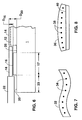
- the edge view of an optical wafer 36 shows varying distances between the machining line 40 and the location of the embedded waveguide paths 38 .
- the term cut refers to the action or result of a tool removing material from a workpiece.
- the term notch refers to a type of cut, wherein the cut is substantially straight and has a cross section in which a horizontal portion is substantially flat.
- the horizontal portion may form, with one or two side walls, either a plateau, e.g., 16 in FIG. 6 , a corner, e.g., 20 in FIG. 6 , or a channel, e.g., 25 in FIG. 6 .
- the present invention overcomes the limitations of the prior art stated above and meets-the need for a precision machining system lower in cost and simpler in concept and design.
- the present invention meets the need for a machining method: which does not require knowledge of the workpiece surface shape prior to locating the surface with a sensor/detector arrangement; in which position data is referenced to a single reference position of the tool so that precision holding or chucking of the workpiece is not required; and, which automatically takes into account tool wear by using the tool as the probe.
- One aspect of the invention is a machined article, having a non-uniform surface, comprising at least one cut made into the surface, wherein the cut depth relative to the surface is substantially constant.
- the cut width is determined by the tool size and the number of passes made along the cut length.
- One embodiment of the invention is a machined optical wafer, having a non-uniform surface, comprising a first and a second notch, said notches having a first and second constant depth relative to the surface.
- the first notch is machined into the wafer along one edge of the wafer.
- the second notch is machined into the wafer adjacent to the first notch and has a depth less than the first notch.
- the two notches machined in this manner form two steps arranged in ascending order from the wafer edge. These two steps may serve as a platform for attaching fiber optic pigtails to the wafer as disclosed, for example, in U. S. patent 4,765,702, Dohan et al.
- FIG. 6 is a side view of this embodiment showing first notch 20 and second notch 16 .
- a preferred depth D16 in this embodiment is about 120 microns, which allows for the target radius of the bare optical fiber and for an adhesive layer.
- Another aspect of the invention is a method for machining a cut into a surface wherein the surface is non-uniform and the depth of the cut relative to the surface is controlled to a target value.
- the method comprises the steps of,
- the positions of contact between tool and workpiece surface are measured relative to the reference or home position of the tool.
- the recorded positions lie along a line so that the cut made using these recorded positions is substantially a notch.
- the means for detecting the contact between tool and surface is an ultrasonic detector attached to the device holding the article.
- the contact generates an ultrasonic wave which is transmitted to the detector.
- the ultrasonic detector generates a signal which is recorded.
- the means for recording the contact signals is connected to machine controlling means, which includes computing means to fit a curve to the recorded contact positions. During machining of a cut, the controlling means controls the movement of the tool to essentially make a cut along the fitted curve.
- a further aspect of the inventive method, wherein the article to be machined is an optical wafer with embedded light paths, is contemplated.
- This aspect of the invention includes the steps, moving a detector to detect light emanating from light paths embedded in the wafer, and recording the location of the detector relative to the cutting tool reference position.
- the tool contact detected by the ultrasonic sensor is used to locate the surface of the wafer.
- the light sensor is used to locate the light path relative to the wafer surface. This information may be used to calculate a curve fit to the contact points which compensates for variations in the embedded depth of the light paths.
- an article which subsequently will undergo one or more machining steps, it is not unusual that the article may be distorted through such mechanisms as thermal cycling or uneven loading during shaping steps.
- An example of such an article, subject to distorting forces during manufacture is a glass wafer with optical waveguide paths created by ion exchange in a wafer surface layer.
- the wafer body is raised to temperatures of about 300 °C to 400 °C. Since the "optical wafer" is typically composed of a substrate with an ion exchanged surface layer, the dissimilar expansion coefficients of the different materials can produce a non-uniformity or warpage in the wafer when it is cooled to room temperature.
- Another method of wafer manufacture is chemical vapor deposition, wherein a multi-layer wafer is formed by photolithographic masking and deposition on a substrate.
- a high temperature step such as the deposition or consolidation step.
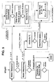
- FIG. 1 is an end view illustration of an optical wafer having a warped arcuate surface 4 .
- FIG. 7 shows a more general non-uniform surface 32 with embedded light paths 34 .
- the following discussion may be applied to either surface shape.
- Embedded in the wafer are optical paths 6 , which, in general, traverse a wafer dimension. These optical paths typically are embedded at a given depth below a surface of the wafer, although some variation in depth of embedding is inherent in the process.
- an optical fiber pigtail is aligned with an optical path in the wafer and fixed in place to receive light from the wafer optical paths.
- the fiber core region must be substantially centered with respect to the optical path output from the wafer.
- the cross sectional dimensions of the wafer optical path and the fiber core region are on the order of 5 to 10 microns.
- the depth to which the optical path is embedded in the wafer is 5 to 10 microns. Total variability of embedded depth of the optical paths in the wafer can be +/- 3 microns.
- the tolerance on the outer glass diameter of the pigtail is +/- 1 to 2 microns.
- warpage of the wafer can be as much as 40 to 50 microns over a wafer dimension of 40 to 60 millimeters.
- the offset of the fiber core center from the wafer lightpath center can be as much as +/- 5 microns. This offset may be reduced by varying the thickness of the adhesive binding the pigtail to the wafer.
- the adhesive thickness which limits require the machining step tolerance to be about +/- 2 microns.
- a thinner glue layer between substrate and pigtail minimizes sensitivity of the endface/output joint to environmental changes.
- the machining must account for warpage of the wafer in order to realize acceptable coupling of light between the fiber and the wafer optical path.
- holding the tight machining tolerance and compensating for the wafer non-uniformity facilitates automatic pigtail alignment. It was noted above in describing the manual prior art that the wafer was segmented before machining. Maintaining the wafer in one piece enhances the automated operation.
- FIG. 2 shows a wafer, having a warped, arcuate surface 10 , fixedly positioned on a holder 12 .
- the method for holding the wafer in place is conventional and is not shown.
- the holder position is fixed relative to the reference position of the tool.
- a rotating cutting tool 2 is shown above the warped surface.
- An ultrasonic detector 8 is attached to holder 12 .
- Ultrasonic detectors such as quartz crystals, are known in the prior art. These detectors have been used, for example, to improve machine utilization by detecting contact between tool and workpiece.
- a fast tool feed rate toward the workpiece is used prior to contact and, upon receiving a contact signal from the detector, a control means slows the tool feed rate as it begins to remove material from the workpiece.
- the arrow pattern at the left of FIG. 2 indicates the tool is free to move relative to the wafer surface.
- the control system diagrammed in FIG. 3 , tracks and records the x,y,z position of the tool.
- a high frequency compressional wave i.e., an ultrasonic wave
- the ultrasonic wave may pass from the workpiece to holder 12 and on to detector 8 .
- Detector 8 converts the ultrasonic wave energy into an electrical pulse which is received by conventional recording means, shown as 9 in FIG. 3 .
- FIG. 3 shows the flow of information into the machine control system.
- Detector 8 sends a signal indicating that a contact between tool and surface has occurred. This signal is received by recorder 9 and sent on to controller 11 .
- Controller 11 stores the point of contact and labels it with coordinates x i ,y i ,z i , measured with respect to the tool reference position, x o ,y o ,z o . For a linear cut one of the three coordinates, which may be chosen as the y coordinate, is held constant.
- Tool 2 shown in FIG. 2 , is retracted and moved to a new point on the wafer surface where another contact is made and another surface point stored and labelled in controller 11 . Successive contact points are stored and labelled so that controller 11 can fit a surface to the points of contact. In general, as the number of contact points increases, the fitted surface more closely approximates the actual wafer surface.
- Controller 11 sends position instructions to tool positioner 15 .
- the position instructions include a start position, an end position and a depth.
- a cut or notch of varying preset depth relative to the contact positions may be made in the wafer.
- the contact positions or points represent the surface of the article, the cut has a depth which is measured relative to that surface.
- the tolerance of the cut depth relative to the surface may be made to meet substantially any specified tolerance by increasing or decreasing the number of contact points recorded to generate the fitted surface.
- controller 11 may feed successive instructions to the positioning machine so that the tool makes a piecewise continuous cut in the surface, wherein the start point for the n+1 segment of the cut is based upon the end point of the n segment of the cut.
- FIG. 4 graphically illustrates an end view of a preferred embodiment of the invention, wherein the contact points lie along a line on the wafer surface.
- the line representing the actual wafer surface 22 is drawn in the z,x coordinate system, with z axis 28 and x axis 26 .
- Three contact points 23 are shown in the z,x coordinate system, where the z i ,x i designations are made relative to a reference position of the tool, z o ,x o , as described above.
- Curve 24 represents the curve fitted to the contact points.
- a target depth D n denoted 30 in FIG. 4 , is entered into computer 11 of FIG. 3 .
- the tool is then instructed to make a cut, having a depth D n , 30 , which follows curve 24 .
- curve 22 varies along axis 28 by more than a few microns over a distance, along axis 26 , of a few millimeters, additional contact points may be required to achieve the desired tolerance on Dn , 30 , relative to the surface 22 .
- the distance 30 between curves 22 and 24 may be held substantially constant over the x-axis traverse 26 .
- only one preset reference point, that of the tool 2 of FIG. 2 and only one reference surface, that of the workpiece or wafer surface, are required. If the wafer surface represented by 22 varies only a few microns over the entire x-axis traversed, then fewer points of contact are required to meet target tolerance on D n .
- the flow chart of FIG. 5 incorporates the major steps, as indicated by the dashed boxes, in the automatic precision machining cycles. These steps are, surface acquisition, machining of a cut having a depth 30 as shown in FIG. 4 , and indexing the tool to machine another cut.
- the surface acquisition step has been described above.
- the acquisition step is shown as a loop, performed N times, thereby acquiring N points on the surface.
- the number of loops, N is programmable. A larger N value is used to obtain a fitted curve which more closely approximates the actual surface shape. Stated differently, the degree of accuracy of fit is programmable.
- the machining step begins by instructing the tool to move to a surface position designated y j ,x i , where y and x define axes in a plane perpendicular to the line of downward movement of the tool.
- the contact point, z i ,x i is referenced to make a cut into the article to a point with coordinates z i -D j ,x i . That is, the tool will cut into the article to a depth D j .
- the tool then cuts along a fitted curve connecting the points, z i -D j ,x i , and z i+1 -D j ,x i+1 .
- the curve fitted between z i -D j ,x i , and z i+1 -D j ,x i+1 is a straight line.
- the tool continues to cut along the fitted curves between contact points until cuts connecting the N contact points have been made.
- the end result is a notch in the surface of the article, where the depth of the notch for the entire length of the notch, is substantially equal to a preset value relative to the surface.
- the notch depth relative to the reference surface may be controlled to a different target at different points along the length of the notch.
- the cutting cycle can be repeated j times using a different starting point on the surface, a different target depth and a different set of contact points or the same set of contact points N. In this manner, a desired number of notches of different target depths may be automatically cut into the wafer.
- the sole preset reference required is the reference position of the tool, as noted above.
- FIG. 6 illustrates a side view of an embodiment of the inventive machined wafer, precision machined according to the inventive method.
- Notch 25 is machined through the waveguide light paths of the wafer, thereby creating outputs for the light paths, having substantially equal mode field diameters.
- Notch 25 also serves as an overflow trough for adhesive.
- Notch 20 is machined to a depth D20 relative to surface 14 , by making the number of adjacent passes required to provide a notch having a total width 23 .
- Notch 16 is machined to a depth D16 relative to surface 14 , by making a first pass adjacent to the last pass of notch 20 and the number of adjacent passes required to reach a notch width 17 .
- notch 20 forms a support for the coated portion 22 of the fiber pigtail.
- Notch 16 forms a support for the bare portion of the fiber 18 .
- the resulting alignment of the pigtail with wafer light path 12 is illustrated.
- the wafer dimensions were 75 x 53 x 3 mm.
- the waveguide paths traversed the 53 mm dimension.
- the maximum processing temperature of the wafer was about 350 °C.
- the 75 x 53 mm surface was warped in an arcuate shape along the 75 mm dimension.
- the maximum deviation of the arcuate surface from a flat reference surface was about 60 microns.
- the 53 mm dimension of the example wafer lies in the plane of the page and the 75 mm dimension is perpendicular to the plane of the page.
- the surface 14 was acquired by making five tool to surface contacts along a line parallel to the 75 mm dimension.
- the contacts were detected by a Movomatic, Gap Control, [Meseltron SA, Division Movomatic, Av. Beauregard 18, CH - 2035, Corcelles, Switzerland], ultrasonic detector and the contact positions, relative to the tool reference position, were recorded and stored as described above.
- a Siemens 810 M, [Siemens, Postfach 4848, D-8500, Nurnberg, Germany], controller was used to store the contact positions and calculate a linear fit for the five contact points.
- Notch 25 was machined to expose the light guide path ends and to provide a trough for excess adhesive.
- Notch 16 was machined to a target depth of 122 microns. Typical deviation from target was +/- 2 microns, with a maximum deviation of about 5 microns.
- the dimension 17 of the notch was 3 mm.
- Notch 20 was machined to a depth of 210 microns with tolerance similar to that of notch 16 .
- Dimension 23 was 2 mm.
- notches were machined into the wafer in a continuous operation. Notches 25 , 16 , and 20 were machined and a corresponding set of three notches were machined into the wafer edge opposite the edge shown in FIG. 6 .
- Optical waveguide fiber pigtails were glued into position on the wafer as illustrated in FIG. 6 and described fully in Dannoux, U.S. patent 4,979,970. The average insertion loss for the 1x16 coupler was measured to be about 14 dB.
- the inventive method is an enabling technology for mass pigtailing or automated pigtailing of optical wafers.
- the fiber pigtail endfaces are brought into close alignment with the corresponding wafer light paths by means of the precision machined notches, thereby eliminating a coarse alignment step in the fiber pigtailing process.
- the inventive method was observed to reduce operator set up time by a factor of nine relative to the manual machining prior art method described above. Machining time was reduced by a factor of two. Furthermore, standard deviation of the cut depth was reduced by a factor of two.
- Some advantages of the inventive method are: it requires only one reference point, the reference position of the tool; all machining is controlled relative to the acquired surface, thereby eliminating the need for a precision holding device; an appreciable cost savings is realized over prior art methods and equipment due to simplicity of the machine and control system; the degree of accuracy of fit is programmable; and the number of cuts and the target cut shape is programmable.
- Compensation for the variation of embedded depth of the light paths may be made by modifying the step of acquiring the surface.
- the modification includes propagating light through the embedded light path and detecting the light emanating from the light path output with a movable detector whose position relative to the reference surface is measured.
- the location of the embedded light paths relative to the reference surface is included with the contact point data in the computer.
- the computer is programmed to take into account the relative light path location, thereby compensating for the variation in depth of the embedded light path.
Landscapes
- Engineering & Computer Science (AREA)
- Automation & Control Theory (AREA)
- General Physics & Mathematics (AREA)
- Physics & Mathematics (AREA)
- Manufacturing & Machinery (AREA)
- Human Computer Interaction (AREA)
- Mechanical Engineering (AREA)
- Inorganic Chemistry (AREA)
- Ceramic Engineering (AREA)
- Chemical & Material Sciences (AREA)
- Grinding And Polishing Of Tertiary Curved Surfaces And Surfaces With Complex Shapes (AREA)
- Constituent Portions Of Griding Lathes, Driving, Sensing And Control (AREA)
- Mechanical Treatment Of Semiconductor (AREA)
- Optical Integrated Circuits (AREA)
- Automatic Control Of Machine Tools (AREA)
Priority Applications (10)
| Application Number | Priority Date | Filing Date | Title |
|---|---|---|---|
| ES93402366T ES2135450T3 (es) | 1993-09-28 | 1993-09-28 | Mecanizado de precision para una oblea de corte. |
| DE69325910T DE69325910T2 (de) | 1993-09-28 | 1993-09-28 | Feine Bearbeitung einer gekrümmten Halbleiterscheibe |
| EP19930402366 EP0645683B1 (de) | 1993-09-28 | 1993-09-28 | Feine Bearbeitung einer gekrümmten Halbleiterscheibe |
| CA 2132116 CA2132116A1 (en) | 1993-09-28 | 1994-09-15 | Precision machining of a warped wafer |
| AU73054/94A AU681896B2 (en) | 1993-09-28 | 1994-09-19 | Precision machining of a warped wafer |
| US08/309,269 US5889911A (en) | 1993-09-28 | 1994-09-20 | Precision machined warped waveguide wafer |
| JP25613194A JPH07164281A (ja) | 1993-09-28 | 1994-09-27 | 加工された物品および物品の表面を加工する方法 |
| CN94116714A CN1111768A (zh) | 1993-09-28 | 1994-09-28 | 翘曲薄片的精密机加工 |
| KR1019940024597A KR950009962A (ko) | 1993-09-28 | 1994-09-28 | 곡면형 웨이퍼의 정밀 가공방법 및 그 가공제품 |
| TW083110249A TW360950B (en) | 1993-09-28 | 1994-11-03 | Precision machining of a warped wafer |
Applications Claiming Priority (1)
| Application Number | Priority Date | Filing Date | Title |
|---|---|---|---|
| EP19930402366 EP0645683B1 (de) | 1993-09-28 | 1993-09-28 | Feine Bearbeitung einer gekrümmten Halbleiterscheibe |
Publications (2)
| Publication Number | Publication Date |
|---|---|
| EP0645683A1 true EP0645683A1 (de) | 1995-03-29 |
| EP0645683B1 EP0645683B1 (de) | 1999-08-04 |
Family
ID=8214750
Family Applications (1)
| Application Number | Title | Priority Date | Filing Date |
|---|---|---|---|
| EP19930402366 Expired - Lifetime EP0645683B1 (de) | 1993-09-28 | 1993-09-28 | Feine Bearbeitung einer gekrümmten Halbleiterscheibe |
Country Status (10)
| Country | Link |
|---|---|
| US (1) | US5889911A (de) |
| EP (1) | EP0645683B1 (de) |
| JP (1) | JPH07164281A (de) |
| KR (1) | KR950009962A (de) |
| CN (1) | CN1111768A (de) |
| AU (1) | AU681896B2 (de) |
| CA (1) | CA2132116A1 (de) |
| DE (1) | DE69325910T2 (de) |
| ES (1) | ES2135450T3 (de) |
| TW (1) | TW360950B (de) |
Families Citing this family (3)
| Publication number | Priority date | Publication date | Assignee | Title |
|---|---|---|---|---|
| DE102007063200B4 (de) * | 2007-12-19 | 2010-10-21 | Kadia Produktion Gmbh + Co. | Verfahren zum Feinbearbeiten mindestens eines Werkstücks mit Hilfe eines Rotationswerkzeugs und eine Feinbearbeitungsvorrichtung |
| JP2013145532A (ja) * | 2012-01-16 | 2013-07-25 | Yaskawa Electric Corp | 加工装置、ツール、加工方法および加工位置の設定方法 |
| US12429701B2 (en) | 2021-12-13 | 2025-09-30 | Samsung Electronics Co., Ltd. | Augmented reality device based on curved waveguide, method therefor, augmented reality glasses based on said device |
Citations (4)
| Publication number | Priority date | Publication date | Assignee | Title |
|---|---|---|---|---|
| EP0308539A1 (de) * | 1987-09-25 | 1989-03-29 | Waldrich Siegen Werkzeugmaschinenbau GmbH | Verfahren zum Ausrichten einer konkreten bzw. wirklichen Fläche, z. B. einer Form, auf ein internes Koordinatensystem einer sich relativ zu ihr bewegenden Maschine, insbesondere einer Mehrachsen-Bandlegemaschine sowie Positionierungssystem bzw. -vorrichtung zur Durchführung des verfahrens |
| WO1989010237A1 (en) * | 1988-04-19 | 1989-11-02 | Renishaw Plc | Apparatus for tracking the surface of a workpiece |
| EP0453391A2 (de) * | 1990-04-20 | 1991-10-23 | United Technologies Corporation | Verfahren zur Herstellung von Turbinenschaufeln |
| EP0482983A1 (de) * | 1990-10-24 | 1992-04-29 | AEROSPATIALE Société Nationale Industrielle | Lokalisierungsvorrichtung für eine ebene Fläche und diese anwendendes Bearbeitungssystem |
Family Cites Families (17)
| Publication number | Priority date | Publication date | Assignee | Title |
|---|---|---|---|---|
| US3967878A (en) * | 1975-03-03 | 1976-07-06 | The United States Of America As Represented By The Secretary Of The Navy | Optical waveguide coupler |
| JPS57173462A (en) * | 1981-04-15 | 1982-10-25 | Yoshiaki Shiono | Detector for instant when tool and material to be worked start to contact with each other |
| US4492362A (en) * | 1982-11-26 | 1985-01-08 | Vetco Offshore, Inc. | Valve seat with trapped O-ring |
| US4534096A (en) * | 1982-11-26 | 1985-08-13 | Vetco Offshore, Inc. | Valve seat with trapped O-ring |
| JPS61279453A (ja) * | 1985-06-03 | 1986-12-10 | Canon Inc | 加工機における被加工物の加工部形状の測定方法 |
| US4783136A (en) * | 1986-04-16 | 1988-11-08 | Gte Laboratories Incorporated | Optical waveguides and methods for making same |
| US4785161A (en) * | 1986-07-21 | 1988-11-15 | Control Data Corporation | Laser machining for producing very small parts |
| US4835361A (en) * | 1986-07-21 | 1989-05-30 | Magnetic Peripherals Inc. | Laser machining for producing very small parts |
| GB2206513B (en) * | 1987-07-08 | 1991-11-06 | Amada Co Ltd | V-shaped groove forming machine and its control method |
| FR2633401B1 (fr) * | 1988-06-24 | 1990-10-05 | Labo Electronique Physique | Dispositif semiconducteur comprenant un guide de lumiere integre qui presente au moins une partie rectiligne et une partie courbe |
| JP2752379B2 (ja) * | 1988-07-08 | 1998-05-18 | ファナック株式会社 | デジタイジング方法 |
| US4954022A (en) * | 1989-06-16 | 1990-09-04 | Underwood Mold Co., Inc. | Method for machining multiple cuts in a workpiece to a uniform depth |
| JPH0348203A (ja) * | 1989-07-15 | 1991-03-01 | Fujitsu Ltd | 光導波路デバイスの形成方法 |
| US5119706A (en) * | 1990-02-12 | 1992-06-09 | Ehrhardt Tool And Machine Company, Inc. | Machine process for chamfering of precision pieces having non-linear edges device therefor |
| JPH03240005A (ja) * | 1990-02-19 | 1991-10-25 | Brother Ind Ltd | 光導波路アレイ |
| JP2544225B2 (ja) * | 1990-02-28 | 1996-10-16 | オークマ株式会社 | キャラクタラインの計測方法及び装置 |
| JPH03293303A (ja) * | 1990-03-26 | 1991-12-25 | Fujitsu Ltd | 集積型位相シフト回折格子とその製造方法および光半導体装置 |
-
1993
- 1993-09-28 DE DE69325910T patent/DE69325910T2/de not_active Expired - Fee Related
- 1993-09-28 ES ES93402366T patent/ES2135450T3/es not_active Expired - Lifetime
- 1993-09-28 EP EP19930402366 patent/EP0645683B1/de not_active Expired - Lifetime
-
1994
- 1994-09-15 CA CA 2132116 patent/CA2132116A1/en not_active Abandoned
- 1994-09-19 AU AU73054/94A patent/AU681896B2/en not_active Ceased
- 1994-09-20 US US08/309,269 patent/US5889911A/en not_active Expired - Lifetime
- 1994-09-27 JP JP25613194A patent/JPH07164281A/ja active Pending
- 1994-09-28 KR KR1019940024597A patent/KR950009962A/ko not_active Withdrawn
- 1994-09-28 CN CN94116714A patent/CN1111768A/zh active Pending
- 1994-11-03 TW TW083110249A patent/TW360950B/zh active
Patent Citations (4)
| Publication number | Priority date | Publication date | Assignee | Title |
|---|---|---|---|---|
| EP0308539A1 (de) * | 1987-09-25 | 1989-03-29 | Waldrich Siegen Werkzeugmaschinenbau GmbH | Verfahren zum Ausrichten einer konkreten bzw. wirklichen Fläche, z. B. einer Form, auf ein internes Koordinatensystem einer sich relativ zu ihr bewegenden Maschine, insbesondere einer Mehrachsen-Bandlegemaschine sowie Positionierungssystem bzw. -vorrichtung zur Durchführung des verfahrens |
| WO1989010237A1 (en) * | 1988-04-19 | 1989-11-02 | Renishaw Plc | Apparatus for tracking the surface of a workpiece |
| EP0453391A2 (de) * | 1990-04-20 | 1991-10-23 | United Technologies Corporation | Verfahren zur Herstellung von Turbinenschaufeln |
| EP0482983A1 (de) * | 1990-10-24 | 1992-04-29 | AEROSPATIALE Société Nationale Industrielle | Lokalisierungsvorrichtung für eine ebene Fläche und diese anwendendes Bearbeitungssystem |
Non-Patent Citations (1)
| Title |
|---|
| "ACTIVE CUTTER FOR MICROMACHINING MLC SUBSTRATES", IBM TECHNICAL DISCLOSURE BULLETIN, vol. 33, no. 1A, June 1990 (1990-06-01), US, pages 194 - 195 * |
Also Published As
| Publication number | Publication date |
|---|---|
| CN1111768A (zh) | 1995-11-15 |
| CA2132116A1 (en) | 1995-03-29 |
| DE69325910T2 (de) | 2000-04-20 |
| DE69325910D1 (de) | 1999-09-09 |
| ES2135450T3 (es) | 1999-11-01 |
| US5889911A (en) | 1999-03-30 |
| AU681896B2 (en) | 1997-09-11 |
| JPH07164281A (ja) | 1995-06-27 |
| KR950009962A (ko) | 1995-04-26 |
| AU7305494A (en) | 1995-04-13 |
| TW360950B (en) | 1999-06-11 |
| EP0645683B1 (de) | 1999-08-04 |
Similar Documents
| Publication | Publication Date | Title |
|---|---|---|
| EP1787176B2 (de) | Maschinenwerkzeug-verfahren | |
| US6865498B2 (en) | System for calibrating the axes on a computer numeric controlled machining system and method thereof | |
| US5387061A (en) | Parameter monitoring compensation system and method | |
| Yandayan et al. | In-process dimensional measurement and control of workpiece accuracy | |
| US5386666A (en) | Automated system for controlling taper length during the lapping of air bearing surface of magnetic heads | |
| GB2163873A (en) | Stylus type touch probe for a machine tool | |
| EP2103376B1 (de) | Schneidvorrichtung für Vibrationsschneiden | |
| US5969817A (en) | Precision indexing angle measuring method and system for machine tools | |
| US5083401A (en) | Method of polishing | |
| US5889911A (en) | Precision machined warped waveguide wafer | |
| EP0068643A2 (de) | Verfahren und Vorrichtung zum Einstellen eines Drehmeissels | |
| CN85105480A (zh) | 针尖接触式探测系统 | |
| JPS6319280B2 (de) | ||
| CN114838685B (zh) | 在机自动跳动分布及初始找正误差检测装置 | |
| JP3873328B2 (ja) | 溝入れ加工方法及び加工装置 | |
| JP2003311589A (ja) | 微細形状の加工方法とその装置 | |
| JP3921758B2 (ja) | 精密溝加工装置 | |
| JP2000263380A (ja) | 工作物の加工方法およびその装置 | |
| JP2607182B2 (ja) | 薄膜型磁気ヘッドの製造装置および製造方法 | |
| JPS6234774A (ja) | 高精度平面研削法 | |
| JPH0319023B2 (de) | ||
| CN120686413A (zh) | 一种光纤阵列自动装配装置及装配方法 | |
| JPH02109662A (ja) | トレーサヘッドの検出誤差の補正方法 | |
| Nagata et al. | Orthogonal-type robot with a CAD/CAM-based position/force controller | |
| JP2001150304A (ja) | 工具長計測装置 |
Legal Events
| Date | Code | Title | Description |
|---|---|---|---|
| PUAI | Public reference made under article 153(3) epc to a published international application that has entered the european phase |
Free format text: ORIGINAL CODE: 0009012 |
|
| AK | Designated contracting states |
Kind code of ref document: A1 Designated state(s): DE ES FR GB IT NL |
|
| 17P | Request for examination filed |
Effective date: 19950826 |
|
| 17Q | First examination report despatched |
Effective date: 19970403 |
|
| GRAG | Despatch of communication of intention to grant |
Free format text: ORIGINAL CODE: EPIDOS AGRA |
|
| GRAG | Despatch of communication of intention to grant |
Free format text: ORIGINAL CODE: EPIDOS AGRA |
|
| GRAH | Despatch of communication of intention to grant a patent |
Free format text: ORIGINAL CODE: EPIDOS IGRA |
|
| GRAH | Despatch of communication of intention to grant a patent |
Free format text: ORIGINAL CODE: EPIDOS IGRA |
|
| GRAA | (expected) grant |
Free format text: ORIGINAL CODE: 0009210 |
|
| AK | Designated contracting states |
Kind code of ref document: B1 Designated state(s): DE ES FR GB IT NL |
|
| REF | Corresponds to: |
Ref document number: 69325910 Country of ref document: DE Date of ref document: 19990909 |
|
| ITF | It: translation for a ep patent filed | ||
| ET | Fr: translation filed | ||
| REG | Reference to a national code |
Ref country code: ES Ref legal event code: FG2A Ref document number: 2135450 Country of ref document: ES Kind code of ref document: T3 |
|
| PLBE | No opposition filed within time limit |
Free format text: ORIGINAL CODE: 0009261 |
|
| STAA | Information on the status of an ep patent application or granted ep patent |
Free format text: STATUS: NO OPPOSITION FILED WITHIN TIME LIMIT |
|
| 26N | No opposition filed | ||
| PGFP | Annual fee paid to national office [announced via postgrant information from national office to epo] |
Ref country code: NL Payment date: 20010618 Year of fee payment: 9 |
|
| PGFP | Annual fee paid to national office [announced via postgrant information from national office to epo] |
Ref country code: GB Payment date: 20010807 Year of fee payment: 9 |
|
| PGFP | Annual fee paid to national office [announced via postgrant information from national office to epo] |
Ref country code: FR Payment date: 20010831 Year of fee payment: 9 |
|
| PGFP | Annual fee paid to national office [announced via postgrant information from national office to epo] |
Ref country code: ES Payment date: 20010919 Year of fee payment: 9 |
|
| PGFP | Annual fee paid to national office [announced via postgrant information from national office to epo] |
Ref country code: DE Payment date: 20010927 Year of fee payment: 9 |
|
| REG | Reference to a national code |
Ref country code: GB Ref legal event code: IF02 |
|
| PG25 | Lapsed in a contracting state [announced via postgrant information from national office to epo] |
Ref country code: GB Free format text: LAPSE BECAUSE OF NON-PAYMENT OF DUE FEES Effective date: 20020928 |
|
| PG25 | Lapsed in a contracting state [announced via postgrant information from national office to epo] |
Ref country code: ES Free format text: LAPSE BECAUSE OF NON-PAYMENT OF DUE FEES Effective date: 20020929 |
|
| PG25 | Lapsed in a contracting state [announced via postgrant information from national office to epo] |
Ref country code: NL Free format text: LAPSE BECAUSE OF NON-PAYMENT OF DUE FEES Effective date: 20030401 Ref country code: DE Free format text: LAPSE BECAUSE OF NON-PAYMENT OF DUE FEES Effective date: 20030401 |
|
| GBPC | Gb: european patent ceased through non-payment of renewal fee |
Effective date: 20020928 |
|
| PG25 | Lapsed in a contracting state [announced via postgrant information from national office to epo] |
Ref country code: FR Free format text: LAPSE BECAUSE OF NON-PAYMENT OF DUE FEES Effective date: 20030603 |
|
| REG | Reference to a national code |
Ref country code: FR Ref legal event code: ST |
|
| REG | Reference to a national code |
Ref country code: ES Ref legal event code: FD2A Effective date: 20031011 |
|
| PG25 | Lapsed in a contracting state [announced via postgrant information from national office to epo] |
Ref country code: IT Free format text: LAPSE BECAUSE OF NON-PAYMENT OF DUE FEES Effective date: 20050928 |