EP0645712A2 - Halbleiterspeichergerät mit Redundanz - Google Patents
Halbleiterspeichergerät mit Redundanz Download PDFInfo
- Publication number
- EP0645712A2 EP0645712A2 EP94114729A EP94114729A EP0645712A2 EP 0645712 A2 EP0645712 A2 EP 0645712A2 EP 94114729 A EP94114729 A EP 94114729A EP 94114729 A EP94114729 A EP 94114729A EP 0645712 A2 EP0645712 A2 EP 0645712A2
- Authority
- EP
- European Patent Office
- Prior art keywords
- fuse
- memory cell
- circuit
- redundancy switching
- circuits
- Prior art date
- Legal status (The legal status is an assumption and is not a legal conclusion. Google has not performed a legal analysis and makes no representation as to the accuracy of the status listed.)
- Granted
Links
Images


Classifications
-
- H—ELECTRICITY
- H04—ELECTRIC COMMUNICATION TECHNIQUE
- H04B—TRANSMISSION
- H04B7/00—Radio transmission systems, i.e. using radiation field
- H04B7/24—Radio transmission systems, i.e. using radiation field for communication between two or more posts
- H04B7/26—Radio transmission systems, i.e. using radiation field for communication between two or more posts at least one of which is mobile
-
- G—PHYSICS
- G11—INFORMATION STORAGE
- G11C—STATIC STORES
- G11C29/00—Checking stores for correct operation ; Subsequent repair; Testing stores during standby or offline operation
- G11C29/70—Masking faults in memories by using spares or by reconfiguring
- G11C29/78—Masking faults in memories by using spares or by reconfiguring using programmable devices
- G11C29/785—Masking faults in memories by using spares or by reconfiguring using programmable devices with redundancy programming schemes
- G11C29/789—Masking faults in memories by using spares or by reconfiguring using programmable devices with redundancy programming schemes using non-volatile cells or latches
-
- G—PHYSICS
- G11—INFORMATION STORAGE
- G11C—STATIC STORES
- G11C29/00—Checking stores for correct operation ; Subsequent repair; Testing stores during standby or offline operation
- G11C29/70—Masking faults in memories by using spares or by reconfiguring
- G11C29/78—Masking faults in memories by using spares or by reconfiguring using programmable devices
- G11C29/80—Masking faults in memories by using spares or by reconfiguring using programmable devices with improved layout
Definitions
- This invention relates to a semiconductor storage device, and more particularly to a semiconductor storage device having memory cells formed from non-volatile transistors.
- the redundancy relief method is a method wherein, for example, spare memory cells for column lines, spare memory cells for row lines, fuse circuits for column line redundancy switching information, fuse circuits for row line redundancy switching information and a redundancy switching control circuit are provided, and redundancy switching information is stored in advance in the fuse circuits. Defective memory cells are replaced with the column line spare memory cells or the row line spare memory cells in accordance with the redundancy switching information.
- a volatile memory integrated circuit such as a DRAM or an SRAM
- polycrystalline silicon is normally used for fuse elements constituting a fuse circuit.
- an inspection step of chips is time consuming because a step of fusing polycrystalline silicon using a laser or some other suitable means to store redundancy switching information is required before the fuse element is enclosed into a package.
- EPROM or a flash memory which is a non-volatile memory integrated circuit
- memory cells are constituted from electrically writable non-volatile transistors.
- a fuse circuit can be constructed using a fuse element constituted from a non-volatile transistor.
- a fuse circuit can be easily used in taking the countermeasure of redundancy switching relief against unacceptable chips.
- a fuse circuit write voltage supply circuit and a fuse circuit write control circuit are required, the area occupied by those peripheral circuits tends to be large.
- Fig. 1 is a block diagram showing an example of a conventional semiconductor storage device having memory cells formed from non-volatile transistors.
- Semiconductor storage device 100 includes two memory cells 1201 and 1202, two column line spare memory cell blocks 1211 and 1212, six row pre-decoders 1101 to 1106, address buffer 111, twelve row decoders 11211 to 11262 from each of which four column lines are outputted, two column selectors 1131 and 1132 from each of which four column lines are outputted, two redundancy switching circuits 1141 and 1142 from each of which a single spare column line is outputted, two sense amplifiers 1151 and 1152, a redundancy switching control circuit 116, a fuse circuit write control circuit 117, six fuse circuits 1181 to 1186, and a fuse circuit write voltage supply circuit 119.
- redundancy switching circuits 1141 and 1142, redundancy switching control circuit 116, fuse circuit write control circuit 117 and fuse circuits 1181 to 1186 function as a redundancy circuit for replacing column line memory cells including defective memory cells produced in memory cell blocks 1201 and 1202 with column line spare memory cells in column line spare memory cell blocks 1211 and 1212.
- column line memory cells denotes four memory cells arranged at cross points between four row lines outputted, for example, from row decoder 11211 and one column line outputted from column selector 1131.
- Memory cell block 1202 on the right side of Fig. 1 is constructed in a similar manner to memory cell block 1201.
- “column line spare memory cells” denotes four spare memory cells arranged, for example, at cross points between four row lines outputted from row decoder 11211 and one spare column line outputted from redundancy switching circuit 1141.
- Column line spare memory block 1212 on the right side of Fig. 1 is constructed in a similar manner to column line spare memory cell block 1211.
- Six row pre-decoders 1101 to 1106 are connected to address buffer 111 by way of first address signal lines L AD1 and select rows of memory cell blocks 1201 and 1202. Twelve row decoders 11211 to 11262 are connected two-to-one to row pre-decoders 1101 to 1106 by way of first to sixth pre-row lines L PC1 to L PC6 , respectively.
- row decoder 11211 and row decoder 11212 are connected to row pre-decoder 1101 by way of first pre-row line L PC1 ; row decoder 11221 and row decoder 11222 are connected to row pre-decoder 1102 by way of second pre-row line L PC2 ; row decoder 11231 and row decoder 11232 are connected to row pre-decoder 1103 by way of third pre-row line L PC3 ; row decoder 11241 and row decoder 11242 are connected to row pre-decoder 1104 by way of fourth pre-row line L PC4 ; row decoder 11251 and row decoder 11252 are connected to row pre-decoder 1105 by way of fifth pre-row line L PC5 ; and row decoder 11261 and row decoder 11262 are connected to row pre-decoder 1106 by way of sixth pre-row line L PC6 .
- Two column selectors 1131 and 1132 are provided to select columns of memory cell blocks 1201 and 1202, respectively.
- column selector 1131 on the left side of Fig. 1 is connected to address buffer 111 by way of first column address signal line L RAD1 and connected to redundancy switching circuit 1141 on the left side of Fig. 1 by way of first data line L D1 .
- column selector 1132 on the right side of Fig. 1 is connected to address buffer 111 by way of first column address signal line L RAD1 and connected to redundancy switching circuit 1142 on the right side of Fig. 1 by way of second data line L D2 .
- the two redundancy switching circuits 1141 and 1142 are provided to replace data from memory cell blocks 1201 and 1202 with data from spare memory cell blocks 1211 and 1212, respectively.
- redundancy switching circuit 1141 on the left side of Fig. 1 is connected to sense amplifier 1151 on the left side of Fig. 1 by way of third data line L D3 and connected to redundancy switching control circuit 116 by way of first control signal line L C1 .
- redundancy switching circuit 1142 on the right side of Fig. 1 is connected to sense amplifier 115P2 on the right side of Fig. 1 by way of fourth data line L D4 and connected to redundancy switching control circuit 116 by way of second control signal line L C2 .
- Redundancy switching control circuit 116 refers to redundancy switching information written in fuse circuits 1181 to 1186 and provides to redundancy switching circuits 1141 and 1142 an instruction as to whether or not data from memory cell blocks 1201 and 1202 should be switched to data from spare memory cell blocks 1211 and 1212, respectively. It is to be noted that redundancy switching control circuit 116 is connected to address buffer 111 by way of second column address signal line L RAD2 and connected to fuse circuits 1181 to 1186 by way of eleventh to sixteenth signal lines L S11 to L S16 , respectively.
- fuse circuits 1181 to 1186 are constituted from fuse elements formed from non-volatile transistors having the same structure as the memory cells described above and are provided so that redundancy switching information may be provided therein. It is to be noted that fuse circuits 1181 to 1186 are connected to fuse circuit write voltage supply circuit 119, and are also connected to fuse circuit write control circuit 117 by way of 21st to 26th signal lines L S21 to L S26 , respectively.
- Fuse circuit write control circuit 117 is provided to write redundancy switching information into fuse circuits 1181 to 1186 and is connected to address circuit 111 by way of second address signal line L AD2 . Meanwhile, fuse circuit write voltage supply circuit 119 is provided to supply to fuse circuits 1181 to 1186 a voltage necessary to write redundancy switching information.
- one of six row pre-decoders 1101 to 1106 is selected in response to a row address signal outputted from address buffer 111 on first address signal line L AD1 . If it is assumed that, for example, row pre-decoder 1101 shown uppermost in Fig. 1 is selected, one of the four row lines outputted from each of row decoders 11211 and 11212 is selected by row decoders 11211 and 11212 which are connected to thus selected row pre-decoder 1101 by way of first pre-row line L PC1 .
- redundancy switching circuit 1141 data switching between data from column selector 1131 and data from column line spare memory cell block 1211 is performed in response to a first control signal outputted from redundancy switching control circuit 116 on first control signal line L C1 , and the data are outputted to sense amplifier 1151 on the left side of Fig. 1.
- Sense amplifier 1151 amplifies the data transmitted thereto from redundancy switching circuit 1141 and outputs the amplified data to an output buffer circuit (not shown).
- Column selector 1132, redundancy switching circuit 1142 and sense amplifier 1152 shown on the right side of Fig. 1 operate in a manner similar to that described above.
- Redundancy switching control circuit 116 produces first and second control signals instructing which column line memory cells of memory cell blocks 1201 and 1202 should be replaced with column line spare memory cells in accordance with the redundancy switching information written in fuse circuits 1181 to 1186.
- the thus-produced first and second control signals are outputted to redundancy switching circuits 1141 and 1142 by way of first and second control signal lines L C1 and L C2 , respectively.
- redundancy switching information instructing the replacement of column line memory cells including the thus-found defective memory cell with column line spare memory cells in column line spare memory cell block 1211 must be written into fuse circuits 1181 to 1186.
- a redundancy switching information write mode a high voltage necessary to write is supplied from fuse circuit write voltage supply circuit 119 to fuse circuits 1181 to 1186, and redundancy switching information is selectively written into fuse circuits 1181 to 1186 by fuse circuit write control circuit 117 in accordance with an address signal outputted from address buffer 111 to second address signal line L AD2 .
- the semiconductor storage device 100 described above (a semiconductor memory integrated circuit such as, for example, an EPROM or a flash memory), while a redundancy switching countermeasure can be easily performed during an inspection step, the necessity for a fuse circuit write voltage supply circuit 119, fuse circuit write control circuit 117 and other circuits tends to increase the area occupied by the peripheral circuits. If large-scale configuration of redundancy circuits is considered in the future, the increase in chip size will result in lower productivity or lower yield in production, with the result that productivity cannot be improved.
- the crucial component in realizing a large-scale redundancy circuit is the fuse circuit write control circuit. While the fuse circuit write control circuit is not directly involved when a user uses the memory product, its function is essential for selecting a fuse circuit into which redundancy switching information should be written for replacing defective memory cells with spare memory cells. Another significant obstacle to reducing chip size is the wiring from the address buffer, since a fuse circuit write control signal necessary to select a fuse circuit by means of the fuse circuit write control circuit is obtained by way of address input terminals.
- a semiconductor storage circuit includes: a memory cell block in which memory cells formed from non-volatile transistors are arranged two-dimensionally, a spare memory cell block constituted from a plurality of spare memory cells to be replaced defective memory cells produced in the memory cell block, a plurality of row pre-decoder circuits for selecting a row of the memory cell block, a plurality of fuse circuits which are constituted from fuse elements formed from non-volatile transistors of the same structure as those of the memory cells and which are adapted to write redundancy switching information therein, a fuse circuit write voltage supply circuit for supplying to the fuse circuits a voltage necessary to write the redundancy switching information, a redundancy switching circuit for switching data from the memory cell block to data from the spare memory cell block, and a redundancy switching control circuit for referring to the redundancy switching information written in the fuse circuits to provide to the redundancy switching circuit an instruction whether or not the data from the memory cell block should be switched to the data from the spare memory cell block; and is
- the plurality of row pre-decoder circuits and the plurality of fuse circuits are connected to each other in a one-by-one corresponding relationship, and one of the plurality of fuse circuits is selected by the plurality of row pre-decoder circuits, and redundancy switching information is written into each fuse circuit. Consequently, there is no necessity for a fuse circuit write control circuit and associated wiring lines which are conventionally required to write redundancy switching information into the fuse circuits.
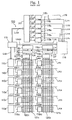
- Fig. 2 is a block diagram showing the construction of an embodiment of a semiconductor storage device of the present invention.
- Semiconductor storage device 1 is different from conventional semiconductor storage device 100 shown in Fig. 1 in that six fuse circuits 181 to 186 are connected in a one-by-one corresponding relationship to six row pre-decoders 101 to 106 by way of first to sixth pre-row lines L PC1 to L PC6 , respectively, and one of the six fuse circuits 181 to 186 is selected by [a corresponding one of the] six row pre-decoders 101 to 106, and redundancy switching information is written into each of fuse circuits 181 to 186.
- redundancy switching information which instructs which column line memory cells of memory cell blocks 201 and 202 should be replaced with column line spare memory cells in column line spare memory cell blocks 211 and 212, is written into fuse circuits 181 to 186 in the following manner.
- Each fuse circuit 181 to 186 is constructed using a fuse element formed from a non-volatile transistor and is capable of having redundancy switching information electrically written into it.
- Selective write control determines the fuse circuit of fuse circuits 181 to 186 into which redundancy switching information should be written and is performed by selecting one of six row pre-decoders 101 to 106 by means of address buffer 11. As an example, when row pre-decoder 101 shown uppermost in Fig.
- fuse circuit 181 which is connected to row pre-decoder 101 by way of first pre-row line L PC1 . It is to be noted that, in this instance, a high voltage necessary to write is supplied from fuse circuit write voltage supply circuit 19 to fuse circuits 181 to 186.
- Redundancy switching control circuit 16 refers to the redundancy switching information written in fuse circuits 181 to 186 and compares the fuse circuit in which the redundancy switching information is written with a column address which was inputted by a user when semiconductor storage device 1 was in a read mode or a write mode. If the column address where defective memory cells are present is used, redundancy switching control circuit 16 outputs to redundancy switching circuits 141 and 142 first and second control signals instructing that column line memory cells including the defective memory cells be replaced with column line spare memory cells in column line spare memory cell blocks 211 and 212, respectively.
- Fig. 3 is a block diagram showing an example of the construction of fuse circuit 181 shown in Fig. 2.
- Fuse circuit 181 includes memory cell 511, first enhancement type transistor 521 formed from nMOS, second enhancement type transistor 531 formed from nMOS, first depletion type transistor 541 formed from nMOS, and second depletion type transistor 551 formed from nMOS.
- memory cell 511 is produced by the same process and has the same structure as the memory cells constituting memory cell blocks 201 and 202 shown in Fig. 2, and the source thereof is grounded.
- the source of first enhancement type transistor 521 is connected to the drain of memory cell 511.
- the source of second enhancement type transistor 531 is connected to the drain of first enhancement type transistor 521.
- the gate of second enhancement type transistor 531 is connected to row pre-decoder 101 by way of input terminal 561 and first pre-row line LPC1 shown in Fig. 2.
- the gate of memory cell 511 and the drain and the gate of second enhancement type transistor 531 are connected independently of one another to fuse circuit write voltage supply circuit 19.
- drain of memory cell 511 is connected to output terminal 571 by way of first depletion type transistor 541, the gate of which is grounded.
- the gate and the drain of second depletion type transistor 551 are connected to output terminal 571, and the source of second depletion type transistor 551 is always held at power source voltage level VCC.
- fuse circuit 181 of the present construction example will next be described.
- redundancy switching information write mode high voltages are supplied independently of one another from fuse circuit write high voltage supply circuit 19 to the gate and the drain of second enhancement type transistor 531 and the gate of memory cell 511. Then, when first pre-row line L PC1 is selected by row pre-decoder 101, a high voltage is applied to the gate of first enhancement type transistor 521 connected to row pre-decoder 101 by way of selected first pre-row line L PC1 . As a result, first enhancement type transistor 521 is turned on. Consequently, the high voltage is applied to the drain of memory cell 511 so that electrons are injected into the floating gate of memory cell 511 to write redundancy switching information into memory cell 511.
- the gate of memory cell 511 is held at power source voltage level V CC by fuse circuit write voltage supply circuit 19, and the gate of second enhancement type transistor 531 is grounded. In this instance, the drain of second enhancement type transistor 531 may be at any potential. If redundancy switching information is written in memory cell 511, memory cell 511 has a high threshold level, and consequently, memory cell 511 is in a non-conducting condition. Accordingly, in this instance, an output signal of a low level is outputted from output terminal 571. In contrast, if redundancy switching information is not written in memory cell 511, the threshold level of memory cell 511 remains as it is, and consequently, memory cell 511 remains in a conducting condition.
- first depletion type transistor 541 acts to prevent the high voltage applied to the drain of memory cell 511 from being applied to output terminal 571 when redundancy switching information is written into memory cell 511.
- fuse circuit 182 to 186 are similar to the construction and operation of fuse circuit 181 described above.
- Fig. 4 is a block diagram showing redundancy switching control circuit block 60 for explaining an example of the construction of the redundancy switching control circuit 16 shown in Fig. 2. It is to be noted that redundancy switching control circuit block 60 shown in Fig. 4 is shown for one circuit for performing column redundancy switching control of each of memory cell blocks 201 and 202, and redundancy switching control circuit 16 is constructed by providing two redundancy switching control circuit blocks 60.
- Redundancy switching control circuit block 60 includes two redundancy switching information comparison circuits 611 and 621 and a three-input NAND circuit 63.
- the output signal of fuse circuit 181 shown in Fig. 2 and column address R AD11 from address buffer 11 are inputted to redundancy switching information comparison circuit 611 shown in the upper portion of Fig. 4.
- the output signal of fuse circuit 182 and column address R AD12 from address buffer 11 are inputted to redundancy switching information comparison circuit 621 shown in the lower portion in Fig. 4.
- the output signals of redundancy switching information comparison circuits 611 and 621 and the output signal of fuse circuit 183 are inputted to NAND circuit 63.
- redundancy switching information regarding a column address in which the defective memory cells are present is written in fuse circuit 181 and fuse circuit 182, and redundancy switching information regarding whether or not redundancy switching control is performed for memory cell blocks 201 and 202 (the redundancy switching information has a high level when redundancy switching control is performed, but has a low level when redundancy switching control is not performed) is written in fuse circuit 183.
- redundancy switching control circuit block 60 of the present construction example The operation of redundancy switching control circuit block 60 of the present construction example will next be described.
- redundancy switching information comparison circuit 611 shown in the upper portion of Fig. 4. When they coincide with each other, an output signal of a high level is outputted, but when they do not coincide with each other, another output signal of a low level is outputted. Meanwhile, redundancy switching information comparison circuit 621 shown in the lower portion in Fig.
- NAND circuit 63 outputs an output signal of a high level when all of the output signals of two redundancy switching information comparison circuits 611 and 621 and the output signal of fuse circuit 183 have a high level, but outputs another output signal of a low level in any other case.
- the output signal of NAND circuit 63 exhibits a low level when the column address from fuse circuit 181 and column address R AD11 coincide with each other and the column address from fuse circuit 182 and column address R AD12 coincide with each other, or when the redundancy switching information from fuse circuit 183 indicates that redundancy switching control is performed.
- the output signal of redundancy switching control circuit block 60 (that is, the output signal of NAND circuit 63) is inputted as a first control signal to redundancy switching circuit 141 by way of first control signal line LC1.
- Redundancy switching circuit 141 outputs data from column line spare memory cell block 211 to sense amplifier 151 when the output signal of redundancy switching control circuit block 60 sent thereto has a low level, but when the output signal of redundancy switching control circuit block 60 sent thereto has a high level, redundancy switching circuit 141 outputs data from memory cell block 201 to sense amplifier 151.
- the output signal of fuse circuit 183, the output signal of fuse circuit 184, the output signal of fuse circuit 185, column address R AD21 and column address R AD22 are inputted to the other redundancy switching control circuit block of redundancy switching control circuit 16, and the output signal of the last-mentioned redundancy switching control circuit block is inputted as a second control signal to redundancy switching circuit 142 by way of second control signal line L C2 .
- the construction and operation of the redundancy switching control circuit block are similar to the construction and operation of redundancy switching control circuit block 60 described above, and accordingly, overlapping description thereof is omitted herein.
- Fig. 5 is a block diagram showing another example of the construction of fuse circuit 181 shown in Fig. 2.
- Fuse circuit 181 of the present construction example is different from fuse circuit 181 of the construction example shown in Fig. 3 in that, in order to allow second enhancement type transistor 531 shown in Fig. 2, which requires larger dimensions, to be provided commonly to fuse circuits 181 to 186, fourth enhancement type transistor 90 formed from nMOS is provided between fuse circuit write voltage supply circuit 19 and fuse circuits 181 to 186. It is to be noted that, since fuse circuit 181 of the present construction example allows realization of fuse circuits 181 to 186 having a smaller area but having the same function, the area occupied by the peripheral circuits can be further reduced.
- Fuse circuit 181 of the present construction example includes memory cell 711, first enhancement transistor 721 formed from nMOS, first depletion type transistor 741 formed from nMOS, second depletion type transistor 751 formed from nMOS, second enhancement type transistor 811 formed from pMOS, and third enhancement type transistor 821 formed from nMOS.
- memory cell 711 is produced by the same process and has the same structure as the memory cells constituting memory cell blocks 201 and 202 shown in Fig. 2, and the source thereof is grounded.
- the source of first enhancement type transistor 721 is connected to the drain of memory cell 711.
- the drain of first enhancement type transistor 721 is connected to the source of fourth enhancement type transistor 90 formed from nMOS.
- the gate of first enhancement type transistor 721 is connected to row pre-decoder 101 by way of second enhancement type transistor 811, input terminal 761 and first pre-row line LPC1 shown in Fig. 2, and is grounded by way of third enhancement type transistor 821.
- the gate of second enhancement type transistor 811 and the gate of third enhancement type transistor 821 are connected to each other.
- the gate of memory cell 711 and the gate of second enhancement type transistor 811 are connected independently of each other to fuse circuit write voltage supply circuit 19. Meanwhile, the drain of memory cell 711 is connected to output terminal 771 by way of first depletion type transistor 741, the gate of which is grounded.
- the gate and the drain of second depletion type transistor 751 are connected to output terminal 771, and the source of second depletion type transistor 751 is normally held at power source voltage level V CC .
- drain and the gate of fourth enhancement type transistor 90 are connected independently of each other to fuse circuit write voltage supply circuit 19.
- fuse circuit 181 of the present construction example will next be described. However, since the operations of memory cell 711, first enhancement type transistor 721, first depletion type transistor 741 and second depletion type transistor 751 are the same as the operations of memory cell 511, first enhancement type transistor 521, first depletion type transistor 541 and second depletion type transistor 551 shown in Fig. 3, overlapping description thereof is omitted.
- a redundancy switching information write mode high voltages for writing are applied from fuse circuit write voltage supply circuit 19 to the gate and the drain of fourth enhancement type transistor 90. Consequently, the gate of fourth enhancement type transistor 90 is set to a high level so that the fourth enhancement type transistor 90 is put into a conducting condition. As a result, a voltage necessary to write redundancy switching information is supplied to fuse circuit 181 connected to the source of fourth enhancement type transistor 90. Further, in this instance, a voltage of a low level is applied from fuse circuit write voltage supply circuit 19 to the gate of second enhancement type transistor 811 and the gate of third enhancement type transistor 821. As a result, second enhancement type transistor 811 is put into a conducting condition and third enhancement type transistor 821 is put into a non-conducting condition. Consequently, write select control of fuse circuit 181 can be performed in response to the output signal of row pre-decoder 101.
- the gate of fourth enhancement type transistor 90 is grounded by fuse circuit write voltage supply circuit 19 so that fourth enhancement type transistor 90 is put into a non-conducting condition.
- the voltage to be applied to the drain of fourth enhancement type transistor 90 may have any potential.
- a voltage of a high level is applied from fuse circuit write voltage supply circuit 19 to the gate of second enhancement type transistor 811 and the gate of third enhancement type transistor 821.
- second enhancement type transistor 811 is put into a non-conducting condition and third enhancement type transistor 821 is put into a conducting condition, and consequently, the gate of first enhancement type transistor 721 normally exhibits a low level.
- Fig. 6 is a block diagram showing the construction of an embodiment wherein column line memory cells including defective memory cells in a memory cell block are replaced with column line spare memory cells in a column line spare memory cell block.
- column pre-decoder circuits 2101 to 2104 and fuse circuits 2181 to 2184 are connected in a one-to-one corresponding relationship to each other similarly to row pre-decoders 101 to 106 and fuse circuits 181 to 186 in the embodiment shown in Fig. 2.
- Row pre-decoder 101, row decoders 1211 and 1212, column selectors 131 and 132, redundancy switching circuits 141 and 142 and sense amplifiers 151 and 152 in Fig. 6 are the same as to those shown in Fig. 2, and although not shown in Fig. 6, the other construction is the samse as to that of the embodiment shown in Fig. 2.
- Column pre-decoder circuits 2101 to 2104 receive an address signal from address buffer 211 to select a fuse circuit. Into the thus-selected fuse circuit, redundancy switching information for a column is written by fuse circuit write voltage supply circuit 219, and redundancy switching control circuit 216 outputs the redundancy switching information written in the fuse circuits to redundancy switching circuits 141 and 142.
- the semiconductor storage device of the present embodiment having the construction described above also exhibits similar effects to those of the embodiment shown in Fig. 1.
- redundancy circuits in the semiconductor storage devices of the present invention described above are constructed so that column line memory cells including defective memory cells in a memory cell block are replaced with column line spare memory cells in a column line spare memory cell block, a similar construction can be employed for, and similar effects are exhibited by, an alternative redundancy circuit wherein row line memory cells including defective memory cells in a memory cell block are replaced with row line spare memory cells in a row line spare memory cell block, or a defective memory cell block in a plurality of memory cell blocks is replaced with a spare memory cell block, or a combination of those constructions is employed. It is to be noted that, while the following two semiconductor storage devices have been proposed as semiconductor storage devices by which reduction of the chip size can be achieved, the semiconductor storage device of the present invention can achieve still further reduction of the chip size.
Landscapes
- Engineering & Computer Science (AREA)
- Computer Networks & Wireless Communication (AREA)
- Signal Processing (AREA)
- For Increasing The Reliability Of Semiconductor Memories (AREA)
- Read Only Memory (AREA)
- Techniques For Improving Reliability Of Storages (AREA)
- Mobile Radio Communication Systems (AREA)
Applications Claiming Priority (3)
| Application Number | Priority Date | Filing Date | Title |
|---|---|---|---|
| JP23638593 | 1993-09-22 | ||
| JP236385/93 | 1993-09-22 | ||
| JP23638593A JP2616544B2 (ja) | 1993-09-22 | 1993-09-22 | 半導体記憶装置 |
Publications (3)
| Publication Number | Publication Date |
|---|---|
| EP0645712A2 true EP0645712A2 (de) | 1995-03-29 |
| EP0645712A3 EP0645712A3 (de) | 1998-11-11 |
| EP0645712B1 EP0645712B1 (de) | 2002-07-03 |
Family
ID=17000000
Family Applications (1)
| Application Number | Title | Priority Date | Filing Date |
|---|---|---|---|
| EP94114729A Expired - Lifetime EP0645712B1 (de) | 1993-09-22 | 1994-09-19 | Halbleiterspeichergerät mit Redundanz |
Country Status (5)
| Country | Link |
|---|---|
| US (1) | US5446693A (de) |
| EP (1) | EP0645712B1 (de) |
| JP (1) | JP2616544B2 (de) |
| KR (2) | KR950009744A (de) |
| DE (1) | DE69430890T2 (de) |
Cited By (1)
| Publication number | Priority date | Publication date | Assignee | Title |
|---|---|---|---|---|
| EP0769743A3 (de) * | 1995-10-18 | 1999-07-28 | Nec Corporation | Halbleiterspeicher mit kleiner Chipgrösse und verkürzter Redundanzzugriffszeit |
Families Citing this family (11)
| Publication number | Priority date | Publication date | Assignee | Title |
|---|---|---|---|---|
| JPH08221993A (ja) * | 1994-03-25 | 1996-08-30 | Seiko Instr Inc | 半導体集積回路装置、その製造方法及びその駆動方法 |
| JPH08335390A (ja) * | 1995-06-08 | 1996-12-17 | Mitsubishi Electric Corp | ダイナミック型半導体記憶装置 |
| US5706292A (en) | 1996-04-25 | 1998-01-06 | Micron Technology, Inc. | Layout for a semiconductor memory device having redundant elements |
| US5966388A (en) * | 1997-01-06 | 1999-10-12 | Micron Technology, Inc. | High-speed test system for a memory device |
| US6172935B1 (en) | 1997-04-25 | 2001-01-09 | Micron Technology, Inc. | Synchronous dynamic random access memory device |
| KR100443527B1 (ko) * | 1999-06-30 | 2004-08-09 | 주식회사 하이닉스반도체 | 로오 리던던시 회로 |
| KR100363085B1 (ko) * | 1999-11-05 | 2002-12-05 | 삼성전자 주식회사 | 리던던시 효율을 향상시키는 로우 리던던시 스킴을 갖는반도체장치 |
| US6339559B1 (en) | 2001-02-12 | 2002-01-15 | International Business Machines Corporation | Decode scheme for programming antifuses arranged in banks |
| KR100659502B1 (ko) * | 2005-02-04 | 2006-12-20 | 삼성전자주식회사 | 플래쉬 셀로 구현한 퓨즈 어레이 회로 |
| JP2007059024A (ja) * | 2005-08-26 | 2007-03-08 | Micron Technol Inc | 温度補償された読み出し・検証動作をフラッシュ・メモリにおいて生成するための方法及び装置 |
| JP2021048230A (ja) * | 2019-09-18 | 2021-03-25 | キオクシア株式会社 | 半導体記憶装置 |
Family Cites Families (5)
| Publication number | Priority date | Publication date | Assignee | Title |
|---|---|---|---|---|
| US5046046A (en) * | 1978-03-10 | 1991-09-03 | Intel Corporation | Redundancy CAM using word line from memory |
| FR2576132B1 (fr) * | 1985-01-15 | 1990-06-29 | Eurotechnique Sa | Memoire en circuit integre |
| US4720817A (en) * | 1985-02-26 | 1988-01-19 | Texas Instruments Incorporated | Fuse selection of predecoder output |
| KR920010347B1 (ko) * | 1989-12-30 | 1992-11-27 | 삼성전자주식회사 | 분할된 워드라인을 가지는 메모리장치의 리던던시 구조 |
| JP2782948B2 (ja) * | 1990-11-16 | 1998-08-06 | 日本電気株式会社 | 半導体メモリ |
-
1993
- 1993-09-22 JP JP23638593A patent/JP2616544B2/ja not_active Expired - Fee Related
-
1994
- 1994-09-17 KR KR1019940023756A patent/KR950009744A/ko active Granted
- 1994-09-17 KR KR1019940023756A patent/KR0140350B1/ko not_active Expired - Fee Related
- 1994-09-19 EP EP94114729A patent/EP0645712B1/de not_active Expired - Lifetime
- 1994-09-19 DE DE69430890T patent/DE69430890T2/de not_active Expired - Fee Related
- 1994-09-22 US US08/310,311 patent/US5446693A/en not_active Expired - Lifetime
Cited By (1)
| Publication number | Priority date | Publication date | Assignee | Title |
|---|---|---|---|---|
| EP0769743A3 (de) * | 1995-10-18 | 1999-07-28 | Nec Corporation | Halbleiterspeicher mit kleiner Chipgrösse und verkürzter Redundanzzugriffszeit |
Also Published As
| Publication number | Publication date |
|---|---|
| KR0140350B1 (ko) | 1998-07-15 |
| KR960012778A (ko) | 1996-04-20 |
| EP0645712B1 (de) | 2002-07-03 |
| EP0645712A3 (de) | 1998-11-11 |
| JPH0793991A (ja) | 1995-04-07 |
| DE69430890D1 (de) | 2002-08-08 |
| US5446693A (en) | 1995-08-29 |
| KR950009744A (ko) | 1995-04-24 |
| JP2616544B2 (ja) | 1997-06-04 |
| DE69430890T2 (de) | 2003-03-13 |
Similar Documents
| Publication | Publication Date | Title |
|---|---|---|
| US5349556A (en) | Row redundancy circuit sharing a fuse box | |
| US5325334A (en) | Column redundancy circuit for a semiconductor memory device | |
| US6094382A (en) | Integrated circuit memory devices with improved layout of fuse boxes and buses | |
| US6650567B1 (en) | Nonvolatile semiconductor memories with a NAND logic cell structure | |
| US5450360A (en) | Flash EEPROM having memory cell arrays supplied respectively with erasing voltage via transfer gates different in current capability from each other | |
| EP0142127A2 (de) | Redundante Schaltung für ein Halbleiterspeichergerät | |
| KR20010049472A (ko) | 글로벌 리던던시를 갖는 메모리소자 | |
| US5847995A (en) | Nonvolatile semiconductor memory device having a plurality of blocks provided on a plurality of electrically isolated wells | |
| US5446693A (en) | Semiconductor storage device | |
| US6144591A (en) | Redundancy selection circuit for semiconductor memories | |
| EP0472209B1 (de) | Halbleiterspeichergerät mit Redundanzschaltung | |
| US4658379A (en) | Semiconductor memory device with a laser programmable redundancy circuit | |
| US20010052599A1 (en) | Semiconductor memory device including plurality of global data lines in parallel arrangement with low parasitic capacitance, and fabrication method thereof | |
| KR100374633B1 (ko) | 리던던시 효율을 향상시키는 칼럼 리던던시 구조를 갖는반도체 메모리 장치 | |
| US4937790A (en) | Semiconductor memory device | |
| US6937532B2 (en) | Semiconductor memory | |
| US5218572A (en) | Semiconductor memory device | |
| US6335897B1 (en) | Semiconductor memory device including redundancy circuit adopting latch cell | |
| KR0172382B1 (ko) | 메모리셀 어레이 블럭의 재배치가 가능한 반도체 메모리 장치 | |
| US5877992A (en) | Data-bit redundancy in semiconductor memories | |
| KR100291132B1 (ko) | 각각의 뱅크에 대한 용장 치환 선택 신호를 출력하기 위한 반도체 메모리 장치 | |
| US6262923B1 (en) | Semiconductor memory device with redundancy function | |
| US6618300B2 (en) | Semiconductor memory device and method for replacing redundancy circuit | |
| US6762971B2 (en) | Semiconductor memory device | |
| KR100536578B1 (ko) | 반도체 메모리 장치 |
Legal Events
| Date | Code | Title | Description |
|---|---|---|---|
| PUAI | Public reference made under article 153(3) epc to a published international application that has entered the european phase |
Free format text: ORIGINAL CODE: 0009012 |
|
| AK | Designated contracting states |
Kind code of ref document: A2 Designated state(s): DE FR GB |
|
| PUAL | Search report despatched |
Free format text: ORIGINAL CODE: 0009013 |
|
| AK | Designated contracting states |
Kind code of ref document: A3 Designated state(s): DE FR GB |
|
| 17P | Request for examination filed |
Effective date: 19981009 |
|
| 17Q | First examination report despatched |
Effective date: 20010328 |
|
| GRAG | Despatch of communication of intention to grant |
Free format text: ORIGINAL CODE: EPIDOS AGRA |
|
| GRAG | Despatch of communication of intention to grant |
Free format text: ORIGINAL CODE: EPIDOS AGRA |
|
| GRAH | Despatch of communication of intention to grant a patent |
Free format text: ORIGINAL CODE: EPIDOS IGRA |
|
| GRAH | Despatch of communication of intention to grant a patent |
Free format text: ORIGINAL CODE: EPIDOS IGRA |
|
| GRAA | (expected) grant |
Free format text: ORIGINAL CODE: 0009210 |
|
| AK | Designated contracting states |
Kind code of ref document: B1 Designated state(s): DE FR GB |
|
| REF | Corresponds to: |
Ref document number: 69430890 Country of ref document: DE Date of ref document: 20020808 |
|
| ET | Fr: translation filed | ||
| REG | Reference to a national code |
Ref country code: GB Ref legal event code: 732E |
|
| PLBE | No opposition filed within time limit |
Free format text: ORIGINAL CODE: 0009261 |
|
| STAA | Information on the status of an ep patent application or granted ep patent |
Free format text: STATUS: NO OPPOSITION FILED WITHIN TIME LIMIT |
|
| 26N | No opposition filed |
Effective date: 20030404 |
|
| REG | Reference to a national code |
Ref country code: FR Ref legal event code: TP |
|
| PGFP | Annual fee paid to national office [announced via postgrant information from national office to epo] |
Ref country code: FR Payment date: 20040908 Year of fee payment: 11 |
|
| PGFP | Annual fee paid to national office [announced via postgrant information from national office to epo] |
Ref country code: GB Payment date: 20040915 Year of fee payment: 11 |
|
| PGFP | Annual fee paid to national office [announced via postgrant information from national office to epo] |
Ref country code: DE Payment date: 20040916 Year of fee payment: 11 |
|
| PG25 | Lapsed in a contracting state [announced via postgrant information from national office to epo] |
Ref country code: GB Free format text: LAPSE BECAUSE OF NON-PAYMENT OF DUE FEES Effective date: 20050919 |
|
| PG25 | Lapsed in a contracting state [announced via postgrant information from national office to epo] |
Ref country code: DE Free format text: LAPSE BECAUSE OF NON-PAYMENT OF DUE FEES Effective date: 20060401 |
|
| GBPC | Gb: european patent ceased through non-payment of renewal fee |
Effective date: 20050919 |
|
| PG25 | Lapsed in a contracting state [announced via postgrant information from national office to epo] |
Ref country code: FR Free format text: LAPSE BECAUSE OF NON-PAYMENT OF DUE FEES Effective date: 20060531 |
|
| REG | Reference to a national code |
Ref country code: FR Ref legal event code: ST Effective date: 20060531 |