EP0645733A2 - Imprimante avec une interface universelle - Google Patents
Imprimante avec une interface universelle Download PDFInfo
- Publication number
- EP0645733A2 EP0645733A2 EP94111343A EP94111343A EP0645733A2 EP 0645733 A2 EP0645733 A2 EP 0645733A2 EP 94111343 A EP94111343 A EP 94111343A EP 94111343 A EP94111343 A EP 94111343A EP 0645733 A2 EP0645733 A2 EP 0645733A2
- Authority
- EP
- European Patent Office
- Prior art keywords
- processor
- interface
- signal line
- printer
- printer according
- Prior art date
- Legal status (The legal status is an assumption and is not a legal conclusion. Google has not performed a legal analysis and makes no representation as to the accuracy of the status listed.)
- Granted
Links
Images
Classifications
-
- G—PHYSICS
- G06—COMPUTING OR CALCULATING; COUNTING
- G06K—GRAPHICAL DATA READING; PRESENTATION OF DATA; RECORD CARRIERS; HANDLING RECORD CARRIERS
- G06K15/00—Arrangements for producing a permanent visual presentation of the output data, e.g. computer output printers
-
- G—PHYSICS
- G06—COMPUTING OR CALCULATING; COUNTING
- G06K—GRAPHICAL DATA READING; PRESENTATION OF DATA; RECORD CARRIERS; HANDLING RECORD CARRIERS
- G06K2215/00—Arrangements for producing a permanent visual presentation of the output data
- G06K2215/0082—Architecture adapted for a particular function
Definitions
- the invention relates to a printer with a universal interface, with a processor which can be connected to a storage medium and data input and output connections for external devices.
- a printer of the generic type has become known from GB 2 211 971 A.
- the processor controlling the entire printing mechanism is connected via a bus to an input and output port as well as to a read-only memory (ROM) and a variable memory (RAM).
- ROM read-only memory
- RAM variable memory
- an interface for an external device, for example a computer, and - separately - a read-only memory (ROM) for font fonts are connected to the input and output port.
- a disadvantage is that the simple printer interface offers only very limited data input and output options.
- external storage media such as electronic memory cards
- Such memory cards can contain data which enable the printer to write with different fonts and must be inserted into the specially provided plug socket on the previously known printer.
- the problem of the present invention is to expand the data input and output options of printers in such a way that data from external storage media, such as e.g. from memory cards into which printers can be read and which can be output to the storage medium.
- the object is achieved by a common interface controlled by the processor, to which both the storage medium and the data input and output connections for external devices can be connected.
- the main idea is to equip the printer with a universal interface to which cards with data input and output connections for external devices as well as storage media can be connected.
- Memory cards can be used, for example, to increase the memory capacity of the printer or to reproduce different fonts based on data stored permanently (in a ROM).
- a graphics card enables the print image to be output to be checked on a screen before it is printed out on the print medium in order to be able to optically identify and remedy any errors.
- the universal interface can be used to connect any input and output cards. The latter can be used in addition to - as a rule, standard - connections for data sources, such as computers, which are not linked to the processor via the interface, but in another way.
- the advantages of the invention consist primarily in the universal expandability of the printer, since any plug-in cards that are already commercially and inexpensively available can be used.
- Cards of this type generally have a write signal line and a read signal line for data input and output connections for external devices, and a write signal line and a read signal line for storage media, so that the interface of the printer is obviously equipped with such lines.
- RISC processors for printers such as an AMD 29200
- a multiplexer recognizes the type of device to be controlled based on the output signal of an address decoder linked to the address bus of the processor and controls the four lines (the write signal line and the read signal line for data input and output connections for external devices as well as the write signal line and the read signal line for storage media) of the interface corresponding.
- the processor can therefore switch between the external device types on the basis of its address bus using the address decoder and the multiplexer.
- plug-in cards with data buses of different widths
- 8 and 16-bit plug-in cards can be used.
- the switchover can be carried out in terms of hardware by a buffer inserted into the bidirectional data bus of the processor, which is controlled by a separate output of the processor and can prevent the transmission of the higher order bits of the data bus (ie switch the latter to high impedance).
- the interface be equipped with a separate baud rate generator as a clock generator in order to be able to operate the processor with any (in particular higher) clock frequency of its own clock generator.
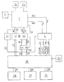
- the basic structure of the circuit consists of a processor (1) which on the one hand controls the actual printing mechanism (25), on the other hand is supplied with the data to be printed by an address bus (11) and a data bus (12) and an interface (20 ), to which different plug-in cards with storage media (26, 27) and data input and output connections (28) for external devices are connected.
- the printing mechanism (25) comprises the mechanical and electronic elements required for printing, that is, as a rule, at least one print head and a motor for feeding the printing medium, which can be, for example, paper or labels applied to a carrier tape.
- the printing mechanism (25) is not shown in the drawing because it is sufficiently well known to the person skilled in the art. If it is a thermal printer, the processor (1) also controls the heating elements of the thermal print head.
- the timing of the processor (1) is defined by a clock (5).
- a data input device (24) which can be designed as a keyboard and / or as an operating panel, is used by the operator to control the processor (1) and thus the printer.
- the decisive innovation of the invention is the use of the interface (20) to which different plug-in cards can be connected by a bus (29 - 31) in a printer.
- the interface (20) enables known and commercially available cards with storage media (26, 27), cards with data input and output connections (28) for external devices (I / O cards, such as, for example, Centronics, RS 232, RS 485 , Network (Ethernet), coaxial or twinax interfaces) or graphics cards with the processor (1).
- I / O cards such as, for example, Centronics, RS 232, RS 485 , Network (Ethernet), coaxial or twinax interfaces
- graphics cards with the processor (1).
- the address bus (11) of the processor (1) is connected to the address bus (13) of the interface (11) via a unidirectional part of a buffer (10), while the data bus (12) of the processor (1) is connected by means of a bidirectional part of the Buffer (10) and another switchable buffer (16) is connected to the interface (20).
- the address of a memory read out by the processor (1) is thus transmitted to the interface (11) via the unidirectional part of the buffer (10); an address transfer in the opposite direction is obvious.
- the data bus (12) of the processor (1) is divided into two on the opposite side of the buffer (10) halves of equal size (generally each comprising 8 bits) are split up and are each transmitted in a separate bus (14, 15) in order to be able to vary the data word width by means of the switchable, also bidirectional buffer (16) (17) switchable buffers (16) controlled by the processor (1) enables the data buses (18, 19) connected to the interface (20) to be looped through to the data buses (14, 15) connected to the buffer (10) to transmit the width of the data bus (usually 16 bits) Alternatively, it is possible to loop through only the bits of the lower order data buses (15, 19) and the higher order data buses (14, 18) to switch off, that is to say to separate them, in order to be able to use plug-in cards (26-28) with less wide data buses at the interface (20).
- the information present on line (17) thus corresponds to
- RISC processor a relatively fast embodiment
- a multiplexer (4) proves to be necessary to control the interface (20).
- the read signal line (2) of the processor (1) is labeled RD ("read") in the drawing, while the write signal line is labeled WR ("write"). If the processor (1) reads in data, a logical one is present on the read signal line (2), whereas a one is present on the write signal line (3) as soon as the processor (1) transmits data to the interface (20).
- the interface itself has four signal lines (6 - 9), one of which can be connected to one.
- the write signal line (6) labeled I / O WR must be connected to one; If the processor (1) reads data from an external device via the interface, the read signal line marked I / O RD must be set to one. Similarly, the write signal line for external storage media (8) is set to one if a memory card connected to the interface (20) is to be written to. Finally, the read signal line MEMRD (9) for external memory cards becomes one as soon as the processor (1) intends to read data from an external memory card.
- the fast processor (1) In order to be able to operate the fast processor (1) with the interface, it controls the address decoder (21) via the address bus (11), which recognizes on the basis of the address present thereon whether the processor (1) has an input or output operation performs peripheral device or on the other hand describes or reads a storage element of an external storage medium.
- the multiplexer (4) controls the four signal lines (6-9) connected to the interface (20) on the basis of the output (22) of the address decoder (21) and the read signal line (2) and the write signal line (3) of the processor (1). If the read signal line (2) of the processor (1) is one and the output (22) of the address decoder (21) shows that a memory operation is being carried out, the multiplexer (4) only connects the MEMRD read signal line (9) for external storage media One.
- the output of the address decoder (21) changes to the opposite logical state and only the I / O RD signal line (7) is set to one.
- the I / O WR or the MEM WR signal lines (6, 8) are set to one, if the Write signal line (3) of the processor (1) is at one. It should be noted that instead of the respective read or write signals, their logical complements can also be present on the lines (2, 3, 6 - 9).
- the interface (20) also has a separate clock generator, the baud rate generator (23).
- the result is a printer that is characterized by its universal applicability and its high processor speed due to its fast processor.
Landscapes
- Engineering & Computer Science (AREA)
- General Engineering & Computer Science (AREA)
- Physics & Mathematics (AREA)
- General Physics & Mathematics (AREA)
- Theoretical Computer Science (AREA)
- Record Information Processing For Printing (AREA)
- Accessory Devices And Overall Control Thereof (AREA)
- Information Transfer Systems (AREA)
- Bus Control (AREA)
Priority Applications (1)
| Application Number | Priority Date | Filing Date | Title |
|---|---|---|---|
| EP98121136A EP0901095A3 (fr) | 1993-09-24 | 1994-07-21 | Imprimante avec une interface universelle |
Applications Claiming Priority (2)
| Application Number | Priority Date | Filing Date | Title |
|---|---|---|---|
| DE4332609 | 1993-09-24 | ||
| DE4332609A DE4332609A1 (de) | 1993-09-24 | 1993-09-24 | Schaltungsanordnung zur Dateneingabe und Datenausgabe für einen Drucker |
Related Child Applications (1)
| Application Number | Title | Priority Date | Filing Date |
|---|---|---|---|
| EP98121136A Division EP0901095A3 (fr) | 1993-09-24 | 1994-07-21 | Imprimante avec une interface universelle |
Publications (3)
| Publication Number | Publication Date |
|---|---|
| EP0645733A2 true EP0645733A2 (fr) | 1995-03-29 |
| EP0645733A3 EP0645733A3 (fr) | 1995-06-28 |
| EP0645733B1 EP0645733B1 (fr) | 1999-06-09 |
Family
ID=6498569
Family Applications (2)
| Application Number | Title | Priority Date | Filing Date |
|---|---|---|---|
| EP98121136A Withdrawn EP0901095A3 (fr) | 1993-09-24 | 1994-07-21 | Imprimante avec une interface universelle |
| EP94111343A Expired - Lifetime EP0645733B1 (fr) | 1993-09-24 | 1994-07-21 | Imprimante avec une interface universelle |
Family Applications Before (1)
| Application Number | Title | Priority Date | Filing Date |
|---|---|---|---|
| EP98121136A Withdrawn EP0901095A3 (fr) | 1993-09-24 | 1994-07-21 | Imprimante avec une interface universelle |
Country Status (6)
| Country | Link |
|---|---|
| US (1) | US5684931A (fr) |
| EP (2) | EP0901095A3 (fr) |
| JP (1) | JPH07210342A (fr) |
| AU (1) | AU669816B2 (fr) |
| DE (2) | DE4332609A1 (fr) |
| SG (1) | SG47103A1 (fr) |
Families Citing this family (10)
| Publication number | Priority date | Publication date | Assignee | Title |
|---|---|---|---|---|
| US6027265A (en) * | 1997-10-14 | 2000-02-22 | Powis Parker, Inc. | Printer having improved print head mechanism and method |
| GB2343658B (en) * | 1998-11-13 | 2002-07-31 | Esselte Nv | A printer with variable friction between printer and a medium |
| US20020138558A1 (en) * | 2001-01-11 | 2002-09-26 | Ferlitsch Andrew R. | Managing and processing print jobs in a networked computer environment |
| US7128236B2 (en) * | 2002-09-13 | 2006-10-31 | Avery Dennison Corporation | Versatile label sheet and dispenser |
| US6991130B2 (en) * | 2002-09-13 | 2006-01-31 | Avery Dennison Corporation | Versatile label sheet and dispenser |
| JP4405223B2 (ja) * | 2003-09-30 | 2010-01-27 | 株式会社キングジム | 文字情報処理システム、文字情報処理装置及び文字情報処理プログラム |
| JP4599827B2 (ja) * | 2003-10-31 | 2010-12-15 | セイコーエプソン株式会社 | テープ印刷装置およびテープ印刷装置のデータ処理方法 |
| JP2008049563A (ja) * | 2006-08-23 | 2008-03-06 | Canon Inc | 画像処理装置、画像記録装置および記録データ生成方法 |
| DE102010009229A1 (de) * | 2010-02-25 | 2011-02-17 | Wavelight Ag | Ärztliche Praxis, insbesondere für augenchirurgische Behandlungen |
| US10350905B2 (en) | 2017-01-26 | 2019-07-16 | Datamax-O'neil Corporation | Detecting printing ribbon orientation |
Family Cites Families (14)
| Publication number | Priority date | Publication date | Assignee | Title |
|---|---|---|---|---|
| DE3680569D1 (de) * | 1985-04-26 | 1991-09-05 | Sato Kk | Thermischer etikettendrucker. |
| US4807177A (en) * | 1986-06-06 | 1989-02-21 | Ward Richard J | Multiple format hand held label printer |
| JPH01118454A (ja) * | 1987-10-30 | 1989-05-10 | Brother Ind Ltd | 印字装置 |
| JPH01187627A (ja) * | 1988-01-22 | 1989-07-27 | Toshiba Corp | 情報処理装置 |
| DE58909413D1 (de) * | 1989-05-31 | 1995-10-05 | Siemens Ag | Adaptereinrichtung zum störungsfreien Anschluss von peripheren Rechnereinrichtungen an eine von Rechnersystemen gesteuerte Peripherieschnittstelle. |
| DE69108443T2 (de) * | 1990-05-17 | 1995-09-21 | Seiko Epson Corp | Streifendrucker. |
| US5150456A (en) * | 1990-08-06 | 1992-09-22 | Elite High Technology, Inc. | Graphic image printing system and method |
| US5110226A (en) * | 1990-10-19 | 1992-05-05 | Norand Corporation | Battery operated data entry terminal device and printer attachment |
| JPH05189104A (ja) * | 1990-10-31 | 1993-07-30 | Ricoh Co Ltd | 並列インタフェース |
| US5195176A (en) * | 1991-09-09 | 1993-03-16 | Destiny Technology Corporation | Method and apparatus to enhance laser printer speed and functionality |
| DE4133998A1 (de) * | 1991-10-14 | 1993-04-15 | Schmidt Anita | Druckerumschalter |
| CA2080608A1 (fr) * | 1992-01-02 | 1993-07-03 | Nader Amini | Logique de commande de bus pour ordinateur a deux bus |
| GB2267984A (en) * | 1992-06-16 | 1993-12-22 | Thorn Emi Electronics Ltd | Multiplexing bus interface. |
| US5358351A (en) * | 1992-09-30 | 1994-10-25 | Casio Computer Co., Ltd. | Printing apparatus and printing tape cassette used therefor |
-
1993
- 1993-09-24 DE DE4332609A patent/DE4332609A1/de not_active Withdrawn
-
1994
- 1994-07-21 SG SG1996007514A patent/SG47103A1/en unknown
- 1994-07-21 EP EP98121136A patent/EP0901095A3/fr not_active Withdrawn
- 1994-07-21 EP EP94111343A patent/EP0645733B1/fr not_active Expired - Lifetime
- 1994-07-21 DE DE59408384T patent/DE59408384D1/de not_active Expired - Fee Related
- 1994-08-16 AU AU70289/94A patent/AU669816B2/en not_active Ceased
- 1994-09-14 JP JP6220283A patent/JPH07210342A/ja active Pending
- 1994-09-22 US US08/310,634 patent/US5684931A/en not_active Expired - Fee Related
Also Published As
| Publication number | Publication date |
|---|---|
| AU669816B2 (en) | 1996-06-20 |
| AU7028994A (en) | 1995-04-06 |
| EP0645733B1 (fr) | 1999-06-09 |
| DE59408384D1 (de) | 1999-07-15 |
| EP0901095A2 (fr) | 1999-03-10 |
| SG47103A1 (en) | 1998-03-20 |
| US5684931A (en) | 1997-11-04 |
| JPH07210342A (ja) | 1995-08-11 |
| EP0645733A3 (fr) | 1995-06-28 |
| DE4332609A1 (de) | 1995-03-30 |
| EP0901095A3 (fr) | 2002-06-12 |
Similar Documents
| Publication | Publication Date | Title |
|---|---|---|
| DE69623607T2 (de) | Vorrichtung und verfahren zur steuerung von peripheriegeräten mit interierter datenkompression | |
| DE69322998T2 (de) | Verfahren und Vorrichtung für die Umwandlung von Bilddaten in einem Printer | |
| DE68927396T2 (de) | Schriftzeichendaten-Steuerung | |
| DE3805573C2 (fr) | ||
| DE69301927T2 (de) | Automatische Bestimmung der Druckerdatenstromsprache | |
| EP0645733B1 (fr) | Imprimante avec une interface universelle | |
| DE4135830C2 (de) | Parallelinterface | |
| EP0056948A1 (fr) | Système de communication pour bureaux | |
| DE69737717T2 (de) | Bildprozessor | |
| DE3716752C2 (fr) | ||
| DE3209187C2 (de) | Verfahren zur Darstellung eines Textes auf einer einzeiligen Anzeigevorrichtung eines Texterstellungsgerätes | |
| DE19525660A1 (de) | Schaltvorrichtung für periphere Komponenten eines Computers | |
| DE3506592C2 (de) | Aufzeichnungsgerät | |
| EP0784901B1 (fr) | Procede et dispositif pour la lecture optique de documents au moyen d'un scanner et pour l'impression d'un support d'enregistrement au moyen d'une imprimante | |
| DE4316278C2 (de) | Einstellsystem für das Betriebsumfeld eines Aufzeichnungsgeräts und Betriebsverfahren für ein Aufzeichnungsgerät | |
| DE3046037A1 (de) | Textbearbeitungsgeraet | |
| DE69634653T2 (de) | Abbildungsausgabegerät und entspechendes Steuerverfahren | |
| DE69428645T2 (de) | Datenbussteuerung mit Pegeleinstellungsschaltung | |
| DE19547995C2 (de) | Seitendrucker-Regelvorrichtung | |
| DE69126259T2 (de) | Druckvorrichtung | |
| EP0895199B1 (fr) | Tachygraphe avec une interface pour sa connexion à un bus de données | |
| DE69222635T2 (de) | Anordnung zum treiben von differentiellen und unsymmetrischen rechnerbussen | |
| EP0338290A2 (fr) | Méthode pour charger une séquence de commandes d'opération nécessaire pour mettre en oeuvre un appareil électrique commandé par un microordinateur | |
| DE69128011T2 (de) | Bilderzeugungsgerät | |
| DE4030324A1 (de) | Ausgabegeraet |
Legal Events
| Date | Code | Title | Description |
|---|---|---|---|
| PUAI | Public reference made under article 153(3) epc to a published international application that has entered the european phase |
Free format text: ORIGINAL CODE: 0009012 |
|
| AK | Designated contracting states |
Kind code of ref document: A2 Designated state(s): DE DK ES FR GB IT NL SE |
|
| PUAL | Search report despatched |
Free format text: ORIGINAL CODE: 0009013 |
|
| AK | Designated contracting states |
Kind code of ref document: A3 Designated state(s): DE DK ES FR GB IT NL SE |
|
| 17P | Request for examination filed |
Effective date: 19950714 |
|
| 17Q | First examination report despatched |
Effective date: 19971216 |
|
| RAP1 | Party data changed (applicant data changed or rights of an application transferred) |
Owner name: METO INTERNATIONAL GMBH |
|
| GRAG | Despatch of communication of intention to grant |
Free format text: ORIGINAL CODE: EPIDOS AGRA |
|
| GRAG | Despatch of communication of intention to grant |
Free format text: ORIGINAL CODE: EPIDOS AGRA |
|
| GRAH | Despatch of communication of intention to grant a patent |
Free format text: ORIGINAL CODE: EPIDOS IGRA |
|
| GRAH | Despatch of communication of intention to grant a patent |
Free format text: ORIGINAL CODE: EPIDOS IGRA |
|
| GRAA | (expected) grant |
Free format text: ORIGINAL CODE: 0009210 |
|
| AK | Designated contracting states |
Kind code of ref document: B1 Designated state(s): DE DK ES FR GB IT NL SE |
|
| PG25 | Lapsed in a contracting state [announced via postgrant information from national office to epo] |
Ref country code: SE Free format text: THE PATENT HAS BEEN ANNULLED BY A DECISION OF A NATIONAL AUTHORITY Effective date: 19990609 Ref country code: IT Free format text: LAPSE BECAUSE OF FAILURE TO SUBMIT A TRANSLATION OF THE DESCRIPTION OR TO PAY THE FEE WITHIN THE PRESCRIBED TIME-LIMIT;WARNING: LAPSES OF ITALIAN PATENTS WITH EFFECTIVE DATE BEFORE 2007 MAY HAVE OCCURRED AT ANY TIME BEFORE 2007. THE CORRECT EFFECTIVE DATE MAY BE DIFFERENT FROM THE ONE RECORDED. Effective date: 19990609 Ref country code: ES Free format text: THE PATENT HAS BEEN ANNULLED BY A DECISION OF A NATIONAL AUTHORITY Effective date: 19990609 |
|
| REF | Corresponds to: |
Ref document number: 59408384 Country of ref document: DE Date of ref document: 19990715 |
|
| ET | Fr: translation filed | ||
| PG25 | Lapsed in a contracting state [announced via postgrant information from national office to epo] |
Ref country code: DK Free format text: LAPSE BECAUSE OF FAILURE TO SUBMIT A TRANSLATION OF THE DESCRIPTION OR TO PAY THE FEE WITHIN THE PRESCRIBED TIME-LIMIT Effective date: 19990909 |
|
| GBT | Gb: translation of ep patent filed (gb section 77(6)(a)/1977) |
Effective date: 19991020 |
|
| PLBE | No opposition filed within time limit |
Free format text: ORIGINAL CODE: 0009261 |
|
| STAA | Information on the status of an ep patent application or granted ep patent |
Free format text: STATUS: NO OPPOSITION FILED WITHIN TIME LIMIT |
|
| 26N | No opposition filed | ||
| REG | Reference to a national code |
Ref country code: GB Ref legal event code: IF02 |
|
| PGFP | Annual fee paid to national office [announced via postgrant information from national office to epo] |
Ref country code: FR Payment date: 20020709 Year of fee payment: 9 |
|
| PGFP | Annual fee paid to national office [announced via postgrant information from national office to epo] |
Ref country code: GB Payment date: 20020717 Year of fee payment: 9 |
|
| PGFP | Annual fee paid to national office [announced via postgrant information from national office to epo] |
Ref country code: DE Payment date: 20020724 Year of fee payment: 9 |
|
| PGFP | Annual fee paid to national office [announced via postgrant information from national office to epo] |
Ref country code: NL Payment date: 20020730 Year of fee payment: 9 |
|
| PG25 | Lapsed in a contracting state [announced via postgrant information from national office to epo] |
Ref country code: GB Free format text: LAPSE BECAUSE OF NON-PAYMENT OF DUE FEES Effective date: 20030721 |
|
| PG25 | Lapsed in a contracting state [announced via postgrant information from national office to epo] |
Ref country code: NL Free format text: LAPSE BECAUSE OF NON-PAYMENT OF DUE FEES Effective date: 20040201 |
|
| PG25 | Lapsed in a contracting state [announced via postgrant information from national office to epo] |
Ref country code: DE Free format text: LAPSE BECAUSE OF NON-PAYMENT OF DUE FEES Effective date: 20040203 |
|
| GBPC | Gb: european patent ceased through non-payment of renewal fee |
Effective date: 20030721 |
|
| PG25 | Lapsed in a contracting state [announced via postgrant information from national office to epo] |
Ref country code: FR Free format text: LAPSE BECAUSE OF NON-PAYMENT OF DUE FEES Effective date: 20040331 |
|
| NLV4 | Nl: lapsed or anulled due to non-payment of the annual fee |
Effective date: 20040201 |
|
| REG | Reference to a national code |
Ref country code: FR Ref legal event code: ST |