EP0645770B1 - Circuit de réglage du niveau zéro du convertisseur A/D dans une unité à disques magnétiques - Google Patents
Circuit de réglage du niveau zéro du convertisseur A/D dans une unité à disques magnétiques Download PDFInfo
- Publication number
- EP0645770B1 EP0645770B1 EP94304873A EP94304873A EP0645770B1 EP 0645770 B1 EP0645770 B1 EP 0645770B1 EP 94304873 A EP94304873 A EP 94304873A EP 94304873 A EP94304873 A EP 94304873A EP 0645770 B1 EP0645770 B1 EP 0645770B1
- Authority
- EP
- European Patent Office
- Prior art keywords
- signal
- zero
- level
- converter
- analog
- Prior art date
- Legal status (The legal status is an assumption and is not a legal conclusion. Google has not performed a legal analysis and makes no representation as to the accuracy of the status listed.)
- Expired - Lifetime
Links
Images




Classifications
-
- H—ELECTRICITY
- H03—ELECTRONIC CIRCUITRY
- H03M—CODING; DECODING; CODE CONVERSION IN GENERAL
- H03M1/00—Analogue/digital conversion; Digital/analogue conversion
- H03M1/12—Analogue/digital converters
- H03M1/124—Sampling or signal conditioning arrangements specially adapted for A/D converters
- H03M1/129—Means for adapting the input signal to the range the converter can handle, e.g. limiting, pre-scaling ; Out-of-range indication
- H03M1/1295—Clamping, i.e. adjusting the DC level of the input signal to a predetermined value
-
- G—PHYSICS
- G11—INFORMATION STORAGE
- G11B—INFORMATION STORAGE BASED ON RELATIVE MOVEMENT BETWEEN RECORD CARRIER AND TRANSDUCER
- G11B20/00—Signal processing not specific to the method of recording or reproducing; Circuits therefor
- G11B20/10—Digital recording or reproducing
- G11B20/10009—Improvement or modification of read or write signals
- G11B20/10037—A/D conversion, D/A conversion, sampling, slicing and digital quantisation or adjusting parameters thereof
-
- G—PHYSICS
- G11—INFORMATION STORAGE
- G11B—INFORMATION STORAGE BASED ON RELATIVE MOVEMENT BETWEEN RECORD CARRIER AND TRANSDUCER
- G11B20/00—Signal processing not specific to the method of recording or reproducing; Circuits therefor
- G11B20/10—Digital recording or reproducing
- G11B20/10009—Improvement or modification of read or write signals
- G11B20/10046—Improvement or modification of read or write signals filtering or equalising, e.g. setting the tap weights of an FIR filter
- G11B20/10203—Improvement or modification of read or write signals filtering or equalising, e.g. setting the tap weights of an FIR filter baseline correction
-
- G—PHYSICS
- G11—INFORMATION STORAGE
- G11B—INFORMATION STORAGE BASED ON RELATIVE MOVEMENT BETWEEN RECORD CARRIER AND TRANSDUCER
- G11B20/00—Signal processing not specific to the method of recording or reproducing; Circuits therefor
- G11B20/10—Digital recording or reproducing
- G11B20/10527—Audio or video recording; Data buffering arrangements
Definitions
- the present invention relates to a zero level setting circuit for an A/D converter in a magnetic disk drive, and particularly, the present invention relates to a zero level setting circuit in a signal processing system of a magnetic disk drive for improving the dynamic range of an A/D converter in the signal processing system to process the read signal in a digital state.
- a magnetic disk drive must be equipped with a demodulator capable of handling signals of high frequency and must have high recording density. These requirements are factors which deteriorate the quality of signals. It is necessary, therefore, to improve not only a system relating to a head and a medium of the magnetic disk drive but also the demodulator of the read signal from the disk so that it can demodulate low-quality signals. For this purpose, a digital demodulating system has been proposed.
- the digital demodulating system employs an A/D converter for converting an input read signal into a digital signal. To improve conversion accuracy, the A/D converter must employ many bits.
- the number of bits of the A/D converter must be as small as possible in terms of circuit scale, power consumption, and heat generation. Accordingly, it is required to provide an A/D converter that can achieve maximum conversion accuracy with a small number of bits.
- JP-A-5-205205 discloses zero-level setting circuitry for use in a magnetic disk drive in which an analog-to-digital converter receives an analog read signal that is produced by processing electrical signals read from a magnetic disk and that has substantially symmetrical positive and negative variations in signal level relative to a zero signal level of the said analog read signal, and in which the converter converts the received analog read signal into a corresponding digital signal for demodulation, the converter having a zero level that is set in dependence upon a reference voltage applied thereto.
- This zero-level setting circuitry may be considered to comprise: reference voltage generating means for generating the said reference voltage; zero-level error detecting means for producing an error signal when said zero level of the converter differs from the said zero signal level of the analog read signal; error signal accumulating means for accumulating the said error signal to produce a correction signal; and zero-level correcting means operable to employ the said correction signal to bring the said zero level of the converter into closer correspondence with the said zero signal level of the analog read signal.
- the error signal is a digital signal which is turned on when an output of the converter falls below a zero-level reference signal provided by a discriminator.
- Zero-level setting circuitry embodying a first aspect of the present invention is characterised in that the zero-level error detecting means has a zero-level detector for detecting a zero-level if the value of the read signal is within a predetermined range of signal values delimited by respective positive and negative signal values, a subtractor for subtracting the reference voltage from the read signal to produce an analog difference signal, and a multiplier for multiplying an output signal of the zero-level detector by the analog difference signal to produce the said error signal.
- Such zero level setting circuitry can maximize the conversion accuracy of the A/D converter even if the A/D converter employs a small number of bits, by equalizing the zero level of a read signal to that of an A/D converter.
- the zero-level-error detector detects an error in the zero level of an input signal to the A/D converter and provides an error signal.
- the error signal the error accumulator, which is made of a loop filter and a charge pump, and the zero-level corrector produce an offset to be applied to the input signal.
- the zero level of the input signal to the A/D converter always agrees with that of the A/D converter, so that the dynamic range of the A/D converter works effectively.
- zero level setting circuitry embodying the present invention can equalize the zero level of a reproduced analog signal in a reproduction system of a magnetic disk drive to the zero level of an A/D converter, so that the A/D converter achieves maximum conversion accuracy with a small number of bits.
- a magnetic disk drive including: signal processing means for reading electrical signals from a magnetic disk and processing the electrical signals to produce an analog read signal that has substantially symmetrical positive and negative variations relative to a zero signal level of the analog read signal; an analog-to-digital converter connected for receiving the said analog read signal and operable to convert that signal into a corresponding digital signal; demodulation means for demodulating the said digital signal; and zero-level setting circuitry embodying the aforesaid first aspect of the present invention for bringing the said zero level of the converter into closer correspondence with the said zero signal level of the analog read signal.
- FIG. 1A is a block circuit diagram showing the construction of a conventional magnetic disk drive.
- a head 1 reads data from a magnetic disk D.
- the read signal is processed by a head amplifier 21, an AGC (automatic gain control) circuit 22, and an LPF (low-pass filter) 23.
- the read signal output from the LPF 23 is an analog signal, which is converted into a digital signal by an A/D converter 6.
- the digital signal is demodulated by a demodulator 7.
- the digital demodulating system requires the A/D converter 6 for converting a read analog signal into a digital signal. To improve the conversion accuracy of the A/D converter 6, it must employ a large number of bits.
- the AGC circuit 22 limits the maximum amplitude of the read signal. If the zero-level of the read signal from the LPF 23 is not equal to the zero level of the A/D converter as shown in Fig. 1B and 1D, it will impair the conversion accuracy. When the zero-level of the read signal from the LPF 23 agrees with the zero level of the A/D converter as shown in Fig. 1C, the conversion accuracy is improved. Contrary to this, when the zero-level of the read signal from the LPF 23 does not agree with a zero level of the A/D converter as shown in Figs. 1B and 1C, the dynamic range is impaired on the positive amplitude side (as shown in Fig. 1B) or negative amplitude side (as shown in Fig. 1D).
- FIG. 2A is a block diagram showing a location of the zero-level setting circuit 10 according to the present invention
- Fig. 4 is a block circuit diagram of a first embodiment of the zero-level setting circuit 10 in Fig. 2A according to the present invention.
- the magnetic disk drive demodulates data recorded in a magnetic disk D.
- the magnetic disk drive has a head 1, a head amplifier 21, an AGC (automatic gain control) circuit 22, an LPF (low-pass filter) 23, an A/D converter 6, and a demodulator 7.
- a zero-level setting circuit 10 embodying the present invention is provided between the LPF 23 and the A/D converter 6.
- the zero-level setting circuit 10 has a reference voltage generator 8, a zero-level-error detector 30, an error accumulator 40, and an adder 50 as a zero-level corrector.
- the reference voltage generator 8 generates a reference voltage Vref.
- the zero-level-error detector 30 detects an error in the zero-level of a read signal (hereinafter referred to as the input signal) Xn from the disk according to the reference voltage Vref.
- the error accumulator 40 accumulates the zero-level error.
- the adder 50 equalizes the zero-level of the A/D converter 6 to the reference voltage Vref according to an output of the error accumulator 40.
- the zero-level-error detector 30 includes a zero-level detector 31, a subtracter 34 and a multiplier 33.
- the zero-level detector 31 detects a zero-level if the input signal Xn is within a predetermined range between positive and negative values.
- the subtracter 34 detects an error in the input signal Xn relative to the reference voltage Vref.
- the multiplier 33 multiplies an output of the zero-level detector 31 by an output of the subtracter 34, to calculate a zero-level error.
- the error accumulator 40 has a loop filter 41, a charge pump (capacitance charge/discharge) circuit 42, and an inverter 43.
- the adder 50 adds an output of the zero-level-error detector 30 to the input signal Xn.
- the zero-level-error detector 30 receives an output of the adder 50 and feeds an output to the error accumulator 40.
- the zero-level detector 31 and subtracter 34 are connected in parallel with each other, to feed their outputs to the multiplier 33.
- the reference voltage generator 8 generates the reference voltage Vref, which is fed to the A/D converter 6 and subtracter 34.
- the zero-level detector 31 receives two decision voltages Vthp and Vthn (Vthp> Vthn) to determine the zero-level of a signal Yn.
- the adder 50 adds an offset to the input signal Xn, to thereby form the signal Yn, which is fed to the A/D converter 6 and zero-level-error detector 30.
- the signal Yn is fed to the zero-level detector 31 and subtracter 34.
- the zero-level detector 31 carries out a three-value test on the signal Yn with use of the decision voltages Vthp and Vthn. Namely, the detector 31 determines if the signal Yn is one of the following three cases:
- the zero-level error ⁇ Vref is fed to the loop filter 41 of the error accumulator 40, which applies a proper time constant to the zero-level error and drives the charge pump circuit 42 that produces an offset voltage.
- the polarity of the offset voltage is inverted by the inverter 43 and is applied to the adder 50, thereby minimizing a difference between the zero-level of an input signal to the A/D converter 6 and the zero-level Vref.
- Figure 3A shows the zero-level detector 31 of Fig. 4, and Fig. 3B shows the operation of the zero-level detector 31.
- the zero-level detector 31 has a first comparator 311, a second comparator 312, and an AND circuit 313.
- a positive input terminal of the first comparator 311 receives the decision voltage Vthp
- a negative input terminal of the second comparator 312 receives the decision voltage Vthn.
- a negative input terminal of the first comparator 311 and a positive input terminal of the second comparator 312 each receive the signal Yn.
- Outputs of the first and the second comparators 311 and 312 are two input terminals of the AND circuit 313.
- the first comparator 311 feeds a high-level output of "1” if the signal Yn is less than the decision voltage Vthp, and the second comparator 312 feeds a high-level output of "1” when the signal Yn is greater than the decision voltage Vthn.
- the comparators 311 and 312 each feed a low-level output of "0".
- the AND circuit 313 feeds a high-level output of "1".only when the signal Yn is greater than the decision voltage Vthn and less than the decision voltage Vthp.
- Figure 3B shows the input characteristic of the signal Yn, and the output characteristic of the signal Yn' of the AND circuit 313. Only when the signal Yn is greater than the decision voltage Vthn and smaller than the decision voltage Vthp at each sampling point (indicated with a black dot) of the signal Yn, does the output signal Yn' of the AND circuit 313 become the high level of "1".
- the adder 50 adds an offset voltage to the input signal Xn and produces the output signal Yn, which is supplied to the A/D converter 6 and zero-level-error detector 30.
- the zero-level-error detector 30 detects an error between the zero-level of the signal Yn and the zero-level Vref of the A/D converter 6.
- the loop filter 41 and charge pump circuit 42 calculate an amount of offset, and the adder 50 adds the offset amount to the input signal Xn. This results in minimizing a difference between the zero-level of the input signal to the A/D converter 6 and the zero-level Vref of the A/D converter 6.
- the range of changes in the input signal Xn agrees with the dynamic range of the A/D converter 6, so that the A/D converter 6 achieves maximum conversion accuracy with a small number of bits.
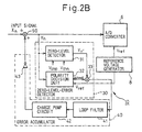
- Fig. 2B is a block diagram showing a zero-level setting circuit 10 not embodying the present invention.
- the zero-level setting circuit of Fig. 2B differs from that of the first embodiment in that it employs a polarity decision unit 32 instead of the subtracter 34 of Fig. 4.
- the same parts as those of Fig. 4 are represented with the same reference marks, and their explanations are not repeated.
- the polarity decision unit 32 compares the signal Yn with the reference voltage Vref, which is equal to the zero-level of the A/D converter 6.
- the zero-level error ⁇ Vref is calculated to be "+1" if Yn - Vref > 0, and "-1" in other cases. This zero-level error is fed to the multiplier 33.
- Figure 5 is a block diagram showing a zero-level setting circuit according to a second embodiment of the present invention.
- the first embodiment and the Fig. 2B circuit add an offset voltage to the input signal Xn, to equalize the zero-level of the input signal Xn to the zero-level of the A/D converter 6.
- the second embodiment directly controls the zero-level Vref of the A/D converter 6, to provide the same effect.
- the second embodiment employs only a zero-level-error detector 30 and an error accumulator 40.
- the arrangements of the zero-level-error detector 30 of the second embodiment are the same as those of the first embodiment.
- the error accumulator 40 produces the reference voltage Vref.
- a loop filter 41 of the error accumulator 40 applies a proper time constant to the zero-level error Vref and drives a charge pump circuit 42, which produces the reference voltage Vref.
- the reference voltage Vref is supplied as it is to the A/D converter 6, thereby equalizing the zero-level of an input signal to the A/D converter 6 to the zero-level of the A/D converter 6.
- this embodiment equalizes the zero-level of the range of changes in the input signal Xn to the zero-level of the A/D converter 6, so that the A/D converter effectively uses the dynamic range of the input signal Xn and achieves maximum conversion accuracy with a small number of bits.
- Fig. 6 is a circuit diagran showing one possible circuit implementation of the adder 50 in either of Figs. 2B & 4.
- the adder 50 for adding an offset to the input signal Xn has transistors Q1 to Q15 and resistors R1 to R18.
- the input signal Xn is received by the transistors Q1 and Q2 that form a differential amplifier.
- An offset voltage from the charge pump is received by the transistors Q3 and Q4 that form a differential amplifier.
- Another input of the differential amplifier of the transistors Q3 and Q4 is connected to a bias source made of the resistors R9 and R10, transistor Q9, and resistor R14.
- the collector side of the differential amplifiers made of the transistors Q1 and Q2, and the collector side of the differential amplifiers made of the transistors Q3 and Q4 are connected to the common load resistors R5 and R6 through the transistors Q5 and Q6.
- Input voltages to each of the differential amplifiers are added in the form of currents and appear between both terminals of the common load resistors R5 and R6.
- the voltage of the collectors is fed outside through an emitter follower made of the transistors Q7 and Q8.
- Fig. 7 is a circuit diagram showing one possible circuit implementation of the subtracter 34 in either of the Figs. 4 and 5 embodiments.
- the subtracter 34 resembles the adder 50 and calculates a difference between the input signal Yn and the reference voltage Vref of the A/D converter 6.
- the subtracter 34 includes transistors Q1 to Q15 and resistors R1 to R18. Unlike the adder 50, a differential amplifier made of the transistors Q1 and Q2 is reversely connected to a differential amplifier made of the transistors Q3 and Q4, to provide a difference between their inputs.
- Fig. 8 is a circuit diagram showing one possible circuit implementation of the multiplier 33in any one of Figs. 2B, 4, and 5.
- the multiplier includes transistors Q1 to Q14 and resistors R1 to R13.
- the multiplier 33 multiplies the signal Yn' of "0" or “1” by the polarity, i.e., the difference Yn - Vref of the input signal Yn.
- the signal Yn' is "1”
- a current from a current source of the transistor Q10 flows through the transistor Q3, to activate a differential amplifier made of the transistors Q1 and Q2.
- the polarity i.e., the difference Yn - Vref is supplied outside through an emitter follower made of the transistors Q7 and Q8.
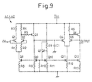
- Fig. 9 is a circuit diagram showing one possible circuit implementation of the loop filter 41 and charge pump circuit 42 in any one of Figs. 2B, 4, and 5. They include transistors Q1 to Q12, resistors R1 to R13, and a capacitor C1.
- the difference Vref is received by a buffer circuit made of the transistors Q1, Q2, and Q3 to charge or discharge the capacitor C1 at low impedance.
- the capacitor C1 produces a voltage, which is supplied to the next stage through a buffer circuit made of the transistors Q4, Q5, and Q6.
- Each of the circuits shown in Figs. 6 to 9 has two input and output systems, so that an analog signal read from the disk is differentially handled. Every analog circuit after the head amplifier is a differential circuit. In the analog circuit, an absolute voltage has no effect and only a difference between two lines is effective. Since this is a known fact, it will not be explained in detail.
- a zero-level setting circuit embodying the present invention equalizes the zero-level of a read analog signal in a reproduction system of a magnetic disk drive to the zero-level of an A/D converter, so that the A/D converter achieves maximum conversion accuracy with a small number of bits.
Landscapes
- Engineering & Computer Science (AREA)
- Signal Processing (AREA)
- Multimedia (AREA)
- Theoretical Computer Science (AREA)
- Analogue/Digital Conversion (AREA)
- Signal Processing For Digital Recording And Reproducing (AREA)
- Digital Magnetic Recording (AREA)
Claims (8)
- Circuit de réglage de niveau zéro, pour une utilisation dans une unité de disque magnétique où un convertisseur analogique-numérique (6) reçoit un signal de lecture analogique (Yn ; Xn) qui est produit en traitant des signaux électriques qui sont lus à partir d'un disque magnétique (D) et qui présente des variations positives et négatives sensiblement symétriques en termes de niveau de signal par rapport à un niveau de signal zéro dudit signal de lecture analogique et dans lequel le convertisseur (6) convertit le signal de lecture analogique reçu selon un signal numérique correspondant pour une démodulation, le convertisseur présentant un niveau zéro qui est réglé en fonction d'une tension de référence (Vref) qui est appliquée dessus, ledit circuit de réglage de niveau zéro (10) comprenant :caractérisé en ce que le moyen de détection d'erreur de niveau zéro (30) comporte un détecteur de niveau zéro (31) pour détecter un niveau zéro si la valeur du signal de lecture est à l'intérieur d'une plage prédéterminée de valeurs de signal qui est délimitée par des valeurs de signal positive et négative respectives (Vthp, Vthn), un soustracteur (34) pour soustraire la tension de référence (Vref) du signal de lecture (Yn ; Xn) afin de produire un signal de différence analogique (ΔVref) et un multiplicateur (33) pour multiplier un signal de sortie du détecteur de niveau zéro (31) par le signal de différence analogique (ΔVref) afin de produire ledit signal d'erreur.un moyen de génération de tension de référence (8 ; 40) pour générer ladite tension de référence (Vref) ;un moyen de détection d'erreur de niveau zéro (30) pour produire un signal d'erreur (ΔVref) lorsque ledit niveau zéro du convertisseur (6) diffère dudit niveau de signal zéro du signal de lecture analogique (Yn ; Xn) ;un moyen d'accumulation de signal d'erreur (40) pour accumuler ledit signal d'erreur (ΔVref) afin de produire un signal de correction (- ; Vref) ; etun moyen de correction de niveau zéro (50 ; 40) qui peut fonctionner pour utiliser ledit signal de correction pour amener ledit niveau zéro du convertisseur (6) selon une correspondance plus proche vis-à-vis dudit niveau de signal zéro du signal de lecture analogique,
- Circuit de réglage de niveau zéro selon la revendication 1, dans lequel :le moyen d'accumulation de signal d'erreur (40) comporte un filtre en boucle (41) et un circuit de charge/décharge de capacité (42) qui coopèrent afin de produire ledit signal de correction ; etledit moyen de correction de niveau zéro (50) comporte un additionneur (50) pour additionner ledit signal de correction au signal de lecture de manière à régler son dit niveau de signal zéro.
- Circuit de réglage de niveau zéro selon la revendication 1, dans lequel ledit moyen d'accumulation de signal d'erreur (40) sert également à régler ladite tension de référence (Vref) en fonction dudit signal de correction de manière à amener ledit niveau zéro du convertisseur (6) selon une correspondance plus proche vis-à-vis dudit niveau de signal zéro du signal de lecture analogique (Yn ; Xn), la tension de référence réglée étant appliquée sur le convertisseur et sur ledit moyen de détection d'erreur de niveau zéro (30).
- Circuit de réglage de niveau zéro selon la revendication 3, dans lequel :le moyen d'accumulation de signal d'erreur (40) comporte un filtre en boucle (41) et un circuit de charge/décharge de capacité (42) qui coopèrent afin de produire ledit signal de correction.
- Circuit de réglage de niveau zéro selon la revendication 3 ou 4, dans lequel ladite tension de référence (Vref) est produite directement par ledit signal de correction.
- Circuit de réglage de niveau zéro selon la revendication 2 ou 4, dans lequel le détecteur de niveau zéro (31) comporte un premier comparateur (311) pour comparer le signal de lecture (Yn ; Xn) avec un premier seuil (Vthp) qui est sur le côté positif de la tension de référence (Vref), un second comparateur (312) pour comparer le signal de lecture avec un second seuil (Vthn) qui est sur le côté négatif de la tension de référence (Vref) et un circuit ET (313) pour soumettre à une logique ET des sorties respectives des premier et second comparateurs (311, 312) afin de produire un signal de décision de niveau zéro "1" du signal de lecture si le signal de lecture est inférieur ou égal au premier seuil (Vthp) et est supérieur ou égal au second seuil (Vthn).
- Circuit de réglage de niveau zéro selon l'une quelconque des revendications précédentes, dans lequel le signal de lecture analogique (Yn; Xn) qui présente des variations positives et négatives sensiblement symétriques par rapport audit niveau de signal zéro est un signal analogique à trois valeurs ou trivaleur.
- Unité de disque magnétique incluant :un moyen de traitement de signal (1, 21 à 23) pour lire des signaux électriques à partir d'un disque magnétique (D) et pour traiter les signaux électriques afin de produire un signal de lecture analogique (Yn ; Xn) qui présente des variations positives et négatives sensiblement symétriques par rapport à un niveau de signal zéro du signal de lecture analogique ;un convertisseur analogique-numérique (6) qui est connecté pour recevoir ledit signal de lecture analogique et qui peut fonctionner pour convertir ce signal selon un signal numérique correspondant ;un moyen de démodulation pour démoduler ledit signal numérique ; etun circuit de réglage de niveau zéro selon l'une quelconque des revendications précédentes pour amener ledit niveau zéro du convertisseur (6) selon une correspondance plus proche vis-à-vis dudit niveau de signal zéro du signal de lecture analogique (Yn ; Xn).
Applications Claiming Priority (3)
| Application Number | Priority Date | Filing Date | Title |
|---|---|---|---|
| JP5238203A JP2809577B2 (ja) | 1993-09-24 | 1993-09-24 | ゼロレベル設定回路 |
| JP238203/93 | 1993-09-24 | ||
| JP23820393 | 1993-09-24 |
Publications (3)
| Publication Number | Publication Date |
|---|---|
| EP0645770A2 EP0645770A2 (fr) | 1995-03-29 |
| EP0645770A3 EP0645770A3 (fr) | 1999-02-17 |
| EP0645770B1 true EP0645770B1 (fr) | 2002-04-03 |
Family
ID=17026690
Family Applications (1)
| Application Number | Title | Priority Date | Filing Date |
|---|---|---|---|
| EP94304873A Expired - Lifetime EP0645770B1 (fr) | 1993-09-24 | 1994-07-04 | Circuit de réglage du niveau zéro du convertisseur A/D dans une unité à disques magnétiques |
Country Status (4)
| Country | Link |
|---|---|
| US (2) | US5602503A (fr) |
| EP (1) | EP0645770B1 (fr) |
| JP (1) | JP2809577B2 (fr) |
| DE (1) | DE69430285T2 (fr) |
Families Citing this family (12)
| Publication number | Priority date | Publication date | Assignee | Title |
|---|---|---|---|---|
| JP2809577B2 (ja) * | 1993-09-24 | 1998-10-08 | 富士通株式会社 | ゼロレベル設定回路 |
| JP3499034B2 (ja) * | 1995-03-13 | 2004-02-23 | 富士通株式会社 | 非対称信号検出回路 |
| JPH08255303A (ja) * | 1995-03-20 | 1996-10-01 | Fujitsu Ltd | アナログ信号の波形整形回路 |
| US6023383A (en) * | 1996-03-19 | 2000-02-08 | Texas Instruments Incorporated | Error estimation circuit and method for providing a read channel error signal |
| US6151178A (en) * | 1996-03-19 | 2000-11-21 | Texas Instruments Incorporated | Error estimation circuit and method using an analog-to-digital converter |
| TW337051B (en) * | 1996-11-29 | 1998-07-21 | Philips Electronics Nv | Analog-to-digital conversion |
| US6121806A (en) * | 1998-10-06 | 2000-09-19 | Mitsubishi Denki Kabushiki Kaisha | Circuit for adjusting a voltage level in a semiconductor device |
| US6739509B2 (en) | 2001-10-03 | 2004-05-25 | Kimberly-Clark Worldwide, Inc. | Registration mark detection using matched filtering |
| US6694205B2 (en) * | 2001-12-21 | 2004-02-17 | Kimberly-Clark Worldwide, Inc. | Binary registration mark detection using 3-state sensing and matched filtering |
| JP2003269378A (ja) * | 2002-03-14 | 2003-09-25 | San Medical Gijutsu Kenkyusho:Kk | 遠心ポンプ |
| US7324162B2 (en) * | 2004-10-13 | 2008-01-29 | Cirrus Logic, Inc. | Method and apparatus to improve ADC dynamic range in a video decoder |
| US9225253B2 (en) * | 2012-10-23 | 2015-12-29 | Microchip Technology Inc. | High voltage switching linear amplifier and method therefor |
Citations (2)
| Publication number | Priority date | Publication date | Assignee | Title |
|---|---|---|---|---|
| JPH05205205A (ja) * | 1992-01-27 | 1993-08-13 | Hitachi Ltd | 再生波形の非線形補正a/d変換方法及び装置 |
| US5418660A (en) * | 1991-12-09 | 1995-05-23 | Hitachi, Ltd. | Information processing apparatus for processing reproduction signal having nonlinear characteristics |
Family Cites Families (11)
| Publication number | Priority date | Publication date | Assignee | Title |
|---|---|---|---|---|
| US3783389A (en) * | 1972-05-31 | 1974-01-01 | Us Army | Median frequency generator |
| US4395671A (en) * | 1979-06-20 | 1983-07-26 | Emhart Industries, Inc. | Control system and method for motor starting |
| US4334185A (en) * | 1980-12-18 | 1982-06-08 | Motorola, Inc. | Circuit for automatic gain control with constant response time |
| US4625240A (en) * | 1984-07-25 | 1986-11-25 | Eeco, Inc. | Adaptive automatic gain control |
| US4924590A (en) * | 1988-01-08 | 1990-05-15 | Siemens Aktiengesellschaft | Method for making metal core printed circuit board |
| JP2543177B2 (ja) * | 1989-03-24 | 1996-10-16 | 松下電器産業株式会社 | クランプ装置と自動利得制御装置 |
| TW258797B (fr) * | 1990-08-24 | 1995-10-01 | Sony Co Ltd | |
| US5084700A (en) * | 1991-02-04 | 1992-01-28 | Thomson Consumer Electronics, Inc. | Signal clamp circuitry for analog-to-digital converters |
| JP3039029B2 (ja) * | 1991-08-09 | 2000-05-08 | ソニー株式会社 | 光ディスクのデータ記録再生方法 |
| JP2809577B2 (ja) * | 1993-09-24 | 1998-10-08 | 富士通株式会社 | ゼロレベル設定回路 |
| US5477183A (en) * | 1994-07-07 | 1995-12-19 | Hughes Aircraft Company | Automatic gain and level control circuit and method |
-
1993
- 1993-09-24 JP JP5238203A patent/JP2809577B2/ja not_active Expired - Fee Related
-
1994
- 1994-07-04 DE DE69430285T patent/DE69430285T2/de not_active Expired - Fee Related
- 1994-07-04 EP EP94304873A patent/EP0645770B1/fr not_active Expired - Lifetime
- 1994-07-06 US US08/267,208 patent/US5602503A/en not_active Expired - Lifetime
-
1996
- 1996-11-08 US US08/745,631 patent/US5731730A/en not_active Expired - Lifetime
Patent Citations (2)
| Publication number | Priority date | Publication date | Assignee | Title |
|---|---|---|---|---|
| US5418660A (en) * | 1991-12-09 | 1995-05-23 | Hitachi, Ltd. | Information processing apparatus for processing reproduction signal having nonlinear characteristics |
| JPH05205205A (ja) * | 1992-01-27 | 1993-08-13 | Hitachi Ltd | 再生波形の非線形補正a/d変換方法及び装置 |
Also Published As
| Publication number | Publication date |
|---|---|
| DE69430285D1 (de) | 2002-05-08 |
| JPH0793896A (ja) | 1995-04-07 |
| US5602503A (en) | 1997-02-11 |
| JP2809577B2 (ja) | 1998-10-08 |
| US5731730A (en) | 1998-03-24 |
| EP0645770A2 (fr) | 1995-03-29 |
| EP0645770A3 (fr) | 1999-02-17 |
| DE69430285T2 (de) | 2002-08-08 |
Similar Documents
| Publication | Publication Date | Title |
|---|---|---|
| EP0645770B1 (fr) | Circuit de réglage du niveau zéro du convertisseur A/D dans une unité à disques magnétiques | |
| US4418406A (en) | Signal wave control circuit | |
| EP0611059B1 (fr) | Système pour récupérer une composante de courant continu pour les signaux binaires transférés en série | |
| US5715110A (en) | Magnetic recording and reproducing apparatus with thermal asperity correction | |
| US4375037A (en) | Receiving circuit | |
| JP2931738B2 (ja) | 音声信号判別装置 | |
| US5986831A (en) | Waveshaping circuit for shaping an analog waveform having unequal positive and negative peak levels so that the positive and negative peak levels are equal | |
| US4706236A (en) | Slice level corrector | |
| US5436771A (en) | Apparatus for correcting a pick-up signal of a digital magnetic recording and reproducing apparatus | |
| EP0393633B1 (fr) | Circuit de restitution de composantes basse fréquence pour la restitution et la compensation de composantes basse fréquence perdues dans un système de transmission de signaux numériques | |
| EP0763887B1 (fr) | Circuit de commande de gain automatique d'un amplificateur différentielle | |
| JPH0765503A (ja) | 情報再生装置におけるアナログ/ディジタル変換回路 | |
| US5815334A (en) | Digital signal detector for correcting signals of a magnetic recording/reproducing device | |
| JP4206517B2 (ja) | 受信装置および受信方法 | |
| JP2625642B2 (ja) | アナログ信号受信回路 | |
| US6278749B1 (en) | Data detector and method for detecting data | |
| JPH0993127A (ja) | 信号処理回路 | |
| JPH1055621A (ja) | 2値化方法、a/d変換方法、2値化装置、及びa/d変換装置 | |
| JPS61261917A (ja) | 直流再生回路 | |
| KR880002694B1 (ko) | 신호 검출장치 | |
| JPH0540976A (ja) | 光磁気記録再生装置の情報再生回路 | |
| JPH0821164B2 (ja) | 磁気テープ再生回路 | |
| JPS58218047A (ja) | デイジタル・オ−デイオ・デイスク・プレ−ヤ用信号検出回路 | |
| JPH07192406A (ja) | タイミングクロック生成用pll装置及びこれを搭載した磁気ディスク装置並びにこれを組み込んだ半導体集積回路 | |
| JPH0131352B2 (fr) |
Legal Events
| Date | Code | Title | Description |
|---|---|---|---|
| PUAI | Public reference made under article 153(3) epc to a published international application that has entered the european phase |
Free format text: ORIGINAL CODE: 0009012 |
|
| AK | Designated contracting states |
Kind code of ref document: A2 Designated state(s): DE GB |
|
| PUAL | Search report despatched |
Free format text: ORIGINAL CODE: 0009013 |
|
| AK | Designated contracting states |
Kind code of ref document: A3 Designated state(s): DE GB |
|
| 17P | Request for examination filed |
Effective date: 19990504 |
|
| 17Q | First examination report despatched |
Effective date: 19990729 |
|
| GRAG | Despatch of communication of intention to grant |
Free format text: ORIGINAL CODE: EPIDOS AGRA |
|
| RTI1 | Title (correction) |
Free format text: ZERO LEVEL SETTING CIRCUIT FOR A/D CONVERTER IN A MAGNETIC DISK DRIVE |
|
| GRAG | Despatch of communication of intention to grant |
Free format text: ORIGINAL CODE: EPIDOS AGRA |
|
| GRAH | Despatch of communication of intention to grant a patent |
Free format text: ORIGINAL CODE: EPIDOS IGRA |
|
| REG | Reference to a national code |
Ref country code: GB Ref legal event code: IF02 |
|
| GRAH | Despatch of communication of intention to grant a patent |
Free format text: ORIGINAL CODE: EPIDOS IGRA |
|
| GRAA | (expected) grant |
Free format text: ORIGINAL CODE: 0009210 |
|
| AK | Designated contracting states |
Kind code of ref document: B1 Designated state(s): DE GB |
|
| REF | Corresponds to: |
Ref document number: 69430285 Country of ref document: DE Date of ref document: 20020508 |
|
| PLBE | No opposition filed within time limit |
Free format text: ORIGINAL CODE: 0009261 |
|
| STAA | Information on the status of an ep patent application or granted ep patent |
Free format text: STATUS: NO OPPOSITION FILED WITHIN TIME LIMIT |
|
| 26N | No opposition filed |
Effective date: 20030106 |
|
| PGFP | Annual fee paid to national office [announced via postgrant information from national office to epo] |
Ref country code: DE Payment date: 20080711 Year of fee payment: 15 |
|
| PGFP | Annual fee paid to national office [announced via postgrant information from national office to epo] |
Ref country code: GB Payment date: 20080709 Year of fee payment: 15 |
|
| GBPC | Gb: european patent ceased through non-payment of renewal fee |
Effective date: 20090704 |
|
| PG25 | Lapsed in a contracting state [announced via postgrant information from national office to epo] |
Ref country code: GB Free format text: LAPSE BECAUSE OF NON-PAYMENT OF DUE FEES Effective date: 20090704 |
|
| PG25 | Lapsed in a contracting state [announced via postgrant information from national office to epo] |
Ref country code: DE Free format text: LAPSE BECAUSE OF NON-PAYMENT OF DUE FEES Effective date: 20100202 |