EP0645819A2 - Mit hoher Dichte integriertes Halbleiterbauelement für hohe Operationsgeschwindigkeiten - Google Patents
Mit hoher Dichte integriertes Halbleiterbauelement für hohe Operationsgeschwindigkeiten Download PDFInfo
- Publication number
- EP0645819A2 EP0645819A2 EP94114655A EP94114655A EP0645819A2 EP 0645819 A2 EP0645819 A2 EP 0645819A2 EP 94114655 A EP94114655 A EP 94114655A EP 94114655 A EP94114655 A EP 94114655A EP 0645819 A2 EP0645819 A2 EP 0645819A2
- Authority
- EP
- European Patent Office
- Prior art keywords
- metal layer
- area
- semiconductor
- semiconductor device
- diffusion area
- Prior art date
- Legal status (The legal status is an assumption and is not a legal conclusion. Google has not performed a legal analysis and makes no representation as to the accuracy of the status listed.)
- Granted
Links
Images


Classifications
-
- H—ELECTRICITY
- H10—SEMICONDUCTOR DEVICES; ELECTRIC SOLID-STATE DEVICES NOT OTHERWISE PROVIDED FOR
- H10W—GENERIC PACKAGES, INTERCONNECTIONS, CONNECTORS OR OTHER CONSTRUCTIONAL DETAILS OF DEVICES COVERED BY CLASS H10
- H10W20/00—Interconnections in chips, wafers or substrates
- H10W20/40—Interconnections external to wafers or substrates, e.g. back-end-of-line [BEOL] metallisations or vias connecting to gate electrodes
-
- H—ELECTRICITY
- H10—SEMICONDUCTOR DEVICES; ELECTRIC SOLID-STATE DEVICES NOT OTHERWISE PROVIDED FOR
- H10W—GENERIC PACKAGES, INTERCONNECTIONS, CONNECTORS OR OTHER CONSTRUCTIONAL DETAILS OF DEVICES COVERED BY CLASS H10
- H10W20/00—Interconnections in chips, wafers or substrates
- H10W20/40—Interconnections external to wafers or substrates, e.g. back-end-of-line [BEOL] metallisations or vias connecting to gate electrodes
- H10W20/41—Interconnections external to wafers or substrates, e.g. back-end-of-line [BEOL] metallisations or vias connecting to gate electrodes characterised by their conductive parts
- H10W20/427—Power or ground buses
-
- H—ELECTRICITY
- H10—SEMICONDUCTOR DEVICES; ELECTRIC SOLID-STATE DEVICES NOT OTHERWISE PROVIDED FOR
- H10W—GENERIC PACKAGES, INTERCONNECTIONS, CONNECTORS OR OTHER CONSTRUCTIONAL DETAILS OF DEVICES COVERED BY CLASS H10
- H10W20/00—Interconnections in chips, wafers or substrates
- H10W20/40—Interconnections external to wafers or substrates, e.g. back-end-of-line [BEOL] metallisations or vias connecting to gate electrodes
- H10W20/41—Interconnections external to wafers or substrates, e.g. back-end-of-line [BEOL] metallisations or vias connecting to gate electrodes characterised by their conductive parts
- H10W20/43—Layouts of interconnections
Definitions
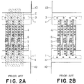
- FIG. 1 illustration is made about an inverter cell, as an example of the conventional semiconductor cell.
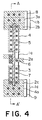
- FIG. 4 illustration is made about an inverter cell, a plurality of which are combined to form the semiconductor device according to the embodiment.
- the first metal layers 1b and 1c overlie whole areas of the p-channel and the n-channel areas 4 and 3.
- the contact holes 7 are provided to cover almost whole areas of the p-channel and the n-channel areas 4 and 3.
- the first metal layers 1b and 1c and the second metal layers 2b and 2c have overlapping areas when considered in a vertical direction.
- the first and the second power supply terminals 8 and 9 consist of the overlapping areas, respectively.
- the first metal layers 1a, 1b, and 1c and the second metal layers 2a, 2b, and 2c are electrically connected to each other by throughholes 6. Except for the first and the second power supply terminals 8 and 9, internal conductor patterns in the semiconductor cell are finished by the first metal layers 1a. Accordingly, electrical interconnection between the semiconductor cells can be readily achieved. Namely, the semiconductor cells are electrically connected to each other by the third metal layer 12 and the interconnecting area of the second metal layer 2a. Particularly, a conductor pattern of the second metal layer for signal transmission can be arranged within a space between the second metal layers 2b and 2c, as symbolized by a broken line block 13 in Fig. 5.
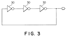
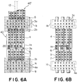
- the semiconductor device 40 comprises three inverter cells (one of which is illustrated in Figs. 4 and 5) to form a ring oscillator circuit, as shown in Fig. 3.
- a conductor pattern arranging area 20 is defined between the power supply line 8 and the ground line 9.
- the conductor pattern arranging area 20 is formed by the above-mentioned spaces symbolized by the broken line block 13 in the three inverter cells.
- the conductor pattern of the second metal layer 2a is arranged, as similarly mentioned before with respect to Fig. 5.
- the semiconductor device 40 for example, an interconnection between the semiconductor cells is accomplished by the second metal layer 2a. As a result, it becomes unnecessary that the second metal layers 2b and 2c are made to be extended up to the both sides of the power supply line 8 and the ground line 9. In other words, the semiconductor device 40 illustrated in Figs. 6A and 6B does not need any patterning spaces at the both sides. Therefore, the semiconductor device 40 does not become so large in size by such patterning spaces.
- adjacent semiconductor devices 40' can be arranged at the both sides in the manner that the semiconductor device 40 has the power supply line 8 or the ground line 9 in common with the adjacent semiconductor devices 40' (in Fig. 6A, illustrated is only an adjacent semiconductor device 40' positioned at the upper side of a sheet of Fig. 6A). Accordingly, it becomes possible that the semiconductor devices 40 are integrated with high density in an IC or an LSI circuit.
- the semiconductor device 40 is electrically connected to the adjacent semiconductor devices 40' by the third metal layer 12, as depicted by a broken line in Fig. 6A. Furthermore, each of input and output terminals of the semiconductor cell can be formed at an optional point in the first metal layers 1b and 1c. Consequently, the interconnection between the semiconductor cells can be freely laid out.
- the delay time in the semiconductor device 40 was 0.9 to 0.95 times less than that of the conventional semiconductor device. Namely, decrease of the delay time was approximately five to ten percentages.
- the semiconductor devices 40 can be integrated with high density in an IC or an LSI circuit, since wiring spaces for power supply or signal lines are considerably reduced in the semiconductor devices 40.
- the semiconductor device is not restricted to such one as comprising CMOS.
- the semiconductor device of the present invention may comprise BiCMOS, nMOS, BinMOS, or the like.
- the connecting portion comprises a plurality of contact holes in the preferred embodiment.
- the connecting portion may comprise a contact hole which covers almost whole of the diffusion area.
Landscapes
- Design And Manufacture Of Integrated Circuits (AREA)
- Semiconductor Integrated Circuits (AREA)
- Internal Circuitry In Semiconductor Integrated Circuit Devices (AREA)
- Metal-Oxide And Bipolar Metal-Oxide Semiconductor Integrated Circuits (AREA)
Applications Claiming Priority (3)
| Application Number | Priority Date | Filing Date | Title |
|---|---|---|---|
| JP238615/93 | 1993-09-27 | ||
| JP23861593 | 1993-09-27 | ||
| JP5238615A JP3057975B2 (ja) | 1993-09-27 | 1993-09-27 | 集積回路の配線 |
Publications (3)
| Publication Number | Publication Date |
|---|---|
| EP0645819A2 true EP0645819A2 (de) | 1995-03-29 |
| EP0645819A3 EP0645819A3 (de) | 1997-12-29 |
| EP0645819B1 EP0645819B1 (de) | 2003-07-16 |
Family
ID=17032806
Family Applications (1)
| Application Number | Title | Priority Date | Filing Date |
|---|---|---|---|
| EP94114655A Expired - Lifetime EP0645819B1 (de) | 1993-09-27 | 1994-09-17 | Mit hoher Dichte integriertes Halbleiterbauelement für hohe Operationsgeschwindigkeiten |
Country Status (4)
| Country | Link |
|---|---|
| US (1) | US5691574A (de) |
| EP (1) | EP0645819B1 (de) |
| JP (1) | JP3057975B2 (de) |
| DE (1) | DE69432946D1 (de) |
Cited By (2)
| Publication number | Priority date | Publication date | Assignee | Title |
|---|---|---|---|---|
| US6785877B1 (en) | 1999-06-28 | 2004-08-31 | Nec Electronics Corporation | Standard cell, standard cell array, and system and method for placing and routing standard cells |
| EP2899755A1 (de) * | 2014-01-22 | 2015-07-29 | MediaTek, Inc | Halbleitergehäuse |
Families Citing this family (9)
| Publication number | Priority date | Publication date | Assignee | Title |
|---|---|---|---|---|
| US20010029079A1 (en) | 1997-03-28 | 2001-10-11 | Nec Corporation | Semiconductor device with multiple emitter contact plugs |
| JP3001045B2 (ja) | 1997-03-28 | 2000-01-17 | 日本電気株式会社 | 半導体装置及びその製造方法 |
| KR100230428B1 (ko) * | 1997-06-24 | 1999-11-15 | 윤종용 | 다층 도전성 패드를 구비하는 반도체장치 및 그 제조방법 |
| US5932928A (en) * | 1997-07-03 | 1999-08-03 | Micron Technology, Inc. | Semiconductor circuit interconnections and methods of making such interconnections |
| US6081033A (en) * | 1997-07-29 | 2000-06-27 | Micron Technology, Inc. | Interconnections for semiconductor circuits |
| US6091090A (en) * | 1997-09-19 | 2000-07-18 | In-Chip Systems, Inc. | Power and signal routing technique for gate array design |
| US5981987A (en) | 1997-12-02 | 1999-11-09 | Nurlogic Design, Inc. | Power ground metallization routing in a semiconductor device |
| JP3523521B2 (ja) * | 1998-04-09 | 2004-04-26 | 松下電器産業株式会社 | Mosトランジスタ対装置 |
| US6137178A (en) * | 1998-06-17 | 2000-10-24 | Siemens Aktiengesellschaft | Semiconductor metalization system and method |
Family Cites Families (12)
| Publication number | Priority date | Publication date | Assignee | Title |
|---|---|---|---|---|
| US4816895A (en) * | 1986-03-06 | 1989-03-28 | Nec Corporation | Integrated circuit device with an improved interconnection line |
| KR0130776B1 (ko) * | 1987-09-19 | 1998-04-06 | 미다 가쓰시게 | 반도체 집적회로 장치 |
| US5223733A (en) * | 1988-10-31 | 1993-06-29 | Hitachi, Ltd. | Semiconductor integrated circuit apparatus and method for designing the same |
| JPH02239646A (ja) * | 1989-03-14 | 1990-09-21 | Fujitsu Ltd | 半導体装置およびその製造方法 |
| US5237199A (en) * | 1989-04-13 | 1993-08-17 | Seiko Epson Corporation | Semiconductor device with interlayer insulating film covering the chip scribe lines |
| JPH03209830A (ja) * | 1990-01-12 | 1991-09-12 | Nec Corp | 半導体記憶回路装置 |
| JPH03248567A (ja) * | 1990-02-27 | 1991-11-06 | Matsushita Electron Corp | 入力保護用トランジスタ |
| US5410173A (en) * | 1991-01-28 | 1995-04-25 | Kikushima; Ken'ichi | Semiconductor integrated circuit device |
| JPH053252A (ja) * | 1991-06-24 | 1993-01-08 | Hitachi Ltd | 半導体集積回路装置 |
| JPH04340252A (ja) * | 1990-07-27 | 1992-11-26 | Mitsubishi Electric Corp | 半導体集積回路装置及びセルの配置配線方法 |
| US5079614A (en) * | 1990-09-26 | 1992-01-07 | S-Mos Systems, Inc. | Gate array architecture with basic cell interleaved gate electrodes |
| JP2840150B2 (ja) * | 1990-12-28 | 1998-12-24 | 川崎製鉄株式会社 | 半導体集積回路及びその層間接続方法 |
-
1993
- 1993-09-27 JP JP5238615A patent/JP3057975B2/ja not_active Expired - Lifetime
-
1994
- 1994-09-17 DE DE69432946T patent/DE69432946D1/de not_active Expired - Lifetime
- 1994-09-17 EP EP94114655A patent/EP0645819B1/de not_active Expired - Lifetime
-
1996
- 1996-09-25 US US08/719,586 patent/US5691574A/en not_active Expired - Lifetime
Cited By (2)
| Publication number | Priority date | Publication date | Assignee | Title |
|---|---|---|---|---|
| US6785877B1 (en) | 1999-06-28 | 2004-08-31 | Nec Electronics Corporation | Standard cell, standard cell array, and system and method for placing and routing standard cells |
| EP2899755A1 (de) * | 2014-01-22 | 2015-07-29 | MediaTek, Inc | Halbleitergehäuse |
Also Published As
| Publication number | Publication date |
|---|---|
| EP0645819B1 (de) | 2003-07-16 |
| DE69432946D1 (de) | 2003-08-21 |
| JP3057975B2 (ja) | 2000-07-04 |
| EP0645819A3 (de) | 1997-12-29 |
| JPH0794682A (ja) | 1995-04-07 |
| US5691574A (en) | 1997-11-25 |
Similar Documents
| Publication | Publication Date | Title |
|---|---|---|
| EP0098163B1 (de) | Gattermatrixchip | |
| JP3154411B2 (ja) | Cadによってレイアウトされた2金属層集積回路ゲート・アレイ | |
| EP0353426B1 (de) | Integrierte Halbleiterschaltungsanordnung mit Leiterschichten | |
| KR100375753B1 (ko) | 반도체 소자의 파워/그라운드 금속 경로 설정 | |
| US5986294A (en) | Semiconductor integrated circuit | |
| EP0645819B1 (de) | Mit hoher Dichte integriertes Halbleiterbauelement für hohe Operationsgeschwindigkeiten | |
| JPH05152529A (ja) | 半導体装置 | |
| US5111271A (en) | Semiconductor device using standard cell system | |
| US5229629A (en) | Semiconductor integrated circuit having improved cell layout | |
| US20010042238A1 (en) | Semiconductor apparatus including bypass capacitor having structure for making automatic design easy, and semiconductor apparatus layout method | |
| KR100306335B1 (ko) | 반도체집적회로장치 | |
| US4750026A (en) | C MOS IC and method of making the same | |
| US6121644A (en) | Semiconductor integrated circuit device and method of arranging and wiring cells | |
| US4943841A (en) | Wiring structure for semiconductor integrated circuit device | |
| US4974049A (en) | Semiconductor integrated circuit configured by using polycell technique | |
| US5063430A (en) | Semiconductor integrated circuit device having standard cells including internal wiring region | |
| US6243286B1 (en) | Semiconductor memory device and method of fabricating the same | |
| US5434436A (en) | Master-slice type semiconductor integrated circuit device having multi-power supply voltage | |
| US4949157A (en) | Large scale integrated circuit | |
| KR920004225B1 (ko) | 마스터 슬라이스(Master slice)방법을 사용하여 반도체 집적회로를 형성하는 방법 | |
| KR950010025A (ko) | 반도체 장치의 설계장치 및 방법 | |
| EP0119059A2 (de) | Integrierte Halbleiterschaltung mit Gattermatrixstruktur | |
| US5422581A (en) | Gate array cell with predefined connection patterns | |
| JP2839722B2 (ja) | 集積回路装置 | |
| JPH10173055A (ja) | セルベース半導体装置及びスタンダードセル |
Legal Events
| Date | Code | Title | Description |
|---|---|---|---|
| PUAI | Public reference made under article 153(3) epc to a published international application that has entered the european phase |
Free format text: ORIGINAL CODE: 0009012 |
|
| AK | Designated contracting states |
Kind code of ref document: A2 Designated state(s): DE FR GB |
|
| PUAL | Search report despatched |
Free format text: ORIGINAL CODE: 0009013 |
|
| AK | Designated contracting states |
Kind code of ref document: A3 Designated state(s): DE FR GB |
|
| 17P | Request for examination filed |
Effective date: 19980330 |
|
| 17Q | First examination report despatched |
Effective date: 20020415 |
|
| GRAH | Despatch of communication of intention to grant a patent |
Free format text: ORIGINAL CODE: EPIDOS IGRA |
|
| GRAH | Despatch of communication of intention to grant a patent |
Free format text: ORIGINAL CODE: EPIDOS IGRA |
|
| GRAA | (expected) grant |
Free format text: ORIGINAL CODE: 0009210 |
|
| AK | Designated contracting states |
Designated state(s): DE FR GB |
|
| PG25 | Lapsed in a contracting state [announced via postgrant information from national office to epo] |
Ref country code: FR Free format text: LAPSE BECAUSE OF FAILURE TO SUBMIT A TRANSLATION OF THE DESCRIPTION OR TO PAY THE FEE WITHIN THE PRESCRIBED TIME-LIMIT Effective date: 20030716 |
|
| REG | Reference to a national code |
Ref country code: GB Ref legal event code: FG4D |
|
| REF | Corresponds to: |
Ref document number: 69432946 Country of ref document: DE Date of ref document: 20030821 Kind code of ref document: P |
|
| PG25 | Lapsed in a contracting state [announced via postgrant information from national office to epo] |
Ref country code: DE Free format text: LAPSE BECAUSE OF FAILURE TO SUBMIT A TRANSLATION OF THE DESCRIPTION OR TO PAY THE FEE WITHIN THE PRESCRIBED TIME-LIMIT Effective date: 20031017 |
|
| PLBE | No opposition filed within time limit |
Free format text: ORIGINAL CODE: 0009261 |
|
| STAA | Information on the status of an ep patent application or granted ep patent |
Free format text: STATUS: NO OPPOSITION FILED WITHIN TIME LIMIT |
|
| 26N | No opposition filed |
Effective date: 20040419 |
|
| EN | Fr: translation not filed | ||
| PGFP | Annual fee paid to national office [announced via postgrant information from national office to epo] |
Ref country code: GB Payment date: 20130911 Year of fee payment: 20 |
|
| REG | Reference to a national code |
Ref country code: GB Ref legal event code: PE20 Expiry date: 20140916 |
|
| PG25 | Lapsed in a contracting state [announced via postgrant information from national office to epo] |
Ref country code: GB Free format text: LAPSE BECAUSE OF EXPIRATION OF PROTECTION Effective date: 20140916 |