EP0645907A2 - Verfahren und Vorrichtung zur Kanalwahl - Google Patents
Verfahren und Vorrichtung zur Kanalwahl Download PDFInfo
- Publication number
- EP0645907A2 EP0645907A2 EP94115225A EP94115225A EP0645907A2 EP 0645907 A2 EP0645907 A2 EP 0645907A2 EP 94115225 A EP94115225 A EP 94115225A EP 94115225 A EP94115225 A EP 94115225A EP 0645907 A2 EP0645907 A2 EP 0645907A2
- Authority
- EP
- European Patent Office
- Prior art keywords
- phase
- channel
- synchronization signal
- reference channel
- data
- Prior art date
- Legal status (The legal status is an assumption and is not a legal conclusion. Google has not performed a legal analysis and makes no representation as to the accuracy of the status listed.)
- Withdrawn
Links
Images






Classifications
-
- H—ELECTRICITY
- H04—ELECTRIC COMMUNICATION TECHNIQUE
- H04J—MULTIPLEX COMMUNICATION
- H04J14/00—Optical multiplex systems
- H04J14/08—Time-division multiplex systems
-
- H—ELECTRICITY
- H04—ELECTRIC COMMUNICATION TECHNIQUE
- H04J—MULTIPLEX COMMUNICATION
- H04J3/00—Time-division multiplex systems
- H04J3/02—Details
- H04J3/06—Synchronising arrangements
- H04J3/0602—Systems characterised by the synchronising information used
Definitions
- the present invention is used for high speed data transmission, and especially for optical fiber data transmission systems that multiplex and distribute high speed data.
- Fig.10 is a block diagram showing the channel selection method described in the above-mentioned Published Unexamined Patent Application.
- 101 is a transmitter.
- 102 to 105 are data transmission circuits for receiving data from data input terminals D1 to D4 respectively and outputting the data at respective timing.
- 106 is a bit multiplexing circuit for time division multiplexing data output from the data transmission circuits 102 to 105 and outputting a serial transmission data to a reception side.
- 107 is a first frequency divider for frequency dividing a transmission clock into 1/4 and supplying pulses of which timing are different each other to the data transmission circuits 102 to 105.
- 108 is a clock generation circuit for supplying the transmission clock to the bit multiplexing circuit 106, the frequency divider 107 and the reception side.
- the 109 is a channel information addition circuit for detecting channel information input from a channel information input terminal CH1 and supplying this channel information to the bit multiplexing circuit 106, the frequency divider 107 and the clock generation circuit 108.
- the channel information consists of channel numbers and information on number of all channels.
- 111 is a data reception circuit for selecting channels in the serial transmission data and extracting data of a specified channel.
- 112 is a clock reception circuit for receiving the transmission clock.
- 113 is a gate circuit for opening and closing at every one clock based on the channel information and channel selection information input into a channel selection input terminal CHS and controlling the transmission clock.
- 114 is a second frequency divider for frequency dividing the clock from the gate circuit 113 into 1/4.
- 115 is a channel information detection circuit for detecting channel information from among reception data.
- OUT is an output terminal of reception data.
- the clock generation circuit 108 generates a clock signal at transmission speed of the system trunk line within the transmitter 101.
- the frequency divider 107 frequency divides the clock signal into 1/4 and supplies the divided clock signals to the data transmission circuits 102 to 105.
- the data transmission circuits 102 to 105 output bit data at different timing in parallel.
- the bit multiplexing circuit 106 time division multiplexes outputs from the data transmission circuits 102 to 105 to make them a serial data.
- the channel information addition circuit 109 receives channel information from the channel information input terminal CH1 and gives channel information to the bit multiplexing circuit 106 via the clock generation circuit 108 and the frequency divider 107.
- the bit multiplexing circuit 106 adds channel information on the above-mentioned serial data to make a serial transmission data and transmits the serial transmission data to the receiver 110 in synchronizing with the transmission clock.
- the data reception circuit 111 in the receiver 110 extracts and receives data of the specified channel from among the serial transmission data transmitted in synchronizing with the above-mentioned transmission clock.
- the synchronization signal used for this extraction operation is the transmission clock, which has been received in the clock reception circuit 112, divided into 1/4 in the frequency divider 114 as shown in Fig.11.
- A is transmission side
- B is reception side
- a is a serial transmission data in which parallel data of channels 1 to 4 are multiplexed
- b is a transmission clock
- c is a transmission clock that is frequency divided into 1/4.
- Fig.12 and Fig.13 are figures to explain channel switching operation.
- a is a transmission clock
- b is a frequency division output output from the frequency divider 114
- c is a serial transmission data.
- channel 1 is switched to channel 4.
- Fig.12 the three clocks, which are drawn by dotted lines on the frequency division output b, show the prohibited clocks, numbers on the serial transmission data c are data according to channel numbers and each channel number marked by a circle shows data of the channel number that is received.
- Fig.13 shows the case of switching channel from channel 3 to channel 1.
- channel 3 is switched to channel 1.
- the transmission side must add all channel information onto a transmission data and the reception side must extract channel information from an arbitrary channel and control channel selection.
- the prior art has a problem that the circuit becomes complicated and the receiver becomes large for signal processing. In addition, if signals of which transmission speed are not same are mixed, the signal processing becomes more complicated.
- a method for channel selection comprising: (a) step of setting at least one channel among N channels as a reference channel, generating a transmission signal by time division multiplexing discrimination information for discriminating the reference channel with data of other channels and transmitting the transmission signal; and (b) step of receiving the transmission signal, detecting temporal location of the reference channel in the N channels based on the discrimination information included in the transmission signal and selecting an arbitrary channel based on a relative time difference between the temporal location of reference channel detected and temporal location of the arbitrary channel in the N channels.
- the channel selection art of the present invention at least one channel among N channels is set as a reference channel and this reference channel is selected after transmitted.
- the present invention features that temporal location of the reference channel in a time division multiplexed data is detected and an arbitrary channel in the N channels is selected.
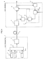
- Fig.1 is a block diagram of the first embodiment of the present invention.
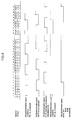
- Fig.2 is a timing chart of the first embodiment of the present invention.
- Fig.3 is a block diagram of the second embodiment of the present invention.
- Fig.4 is a block diagram of the third embodiment of the present invention.
- Fig.5 is a block diagram of the fourth embodiment of the present invention.
- Fig.6 is a timing chart of the fourth embodiment of the present invention.
- Fig.7 is a block diagram of the fifth embodiment of the present invention.
- Fig.8 is a timing chart of the fifth embodiment of the present invention.
- Fig.9 is a timing chart of the fifth embodiment of the present invention.
- Fig.10 is a figure for explaining a prior art.
- Fig.11 is a figure for explaining a prior art.
- Fig.12 is a figure for explaining a prior art.
- Fig.13 is a figure for explaining a prior art.
- the first embodiment is a case that (N-1) channels and a reference channel are supposed and all of these channels are time division multiplexed in the same transmission speed.
- Fig.1 is a block diagram of the first embodiment.
- A is a data transmitter
- B is a data receiver
- c is a synchronization signal phase control means.
- This discrimination information 1a is a fixed cyclic pulse string, for example, 101010 ?? .
- the channel having this discrimination information generator 1 is a reference channel.
- 21 to 2 n-1 are (N-1) data generators for generating data 21a to 2 n-1 a, respectively.
- 3 is a time division multiplexing circuit for time division multiplexing the discrimination information 1a and data 21a to 2 n-2 a.
- 6 is an optical receiver for converting a light signal transmitted to electric information.
- a transmission clock signal extraction circuit for extracting a transmission clock signal from the electric information.
- synchronization signal phase changing circuit for changing phase of the synchronization signal according to an instruction from a synchronization signal phase control circuit 12 described later.
- a data extraction circuit for selecting a channel synchronized with phase of a synchronization signal from the synchronization signal phase changing circuit 9 and extracting data of the channel.
- 11 is a reference channel detection circuit for monitoring each output of the channel output from the data extraction circuit 10 and detecting a reference channel by discriminating a signal string of discrimination information.
- synchronization signal phase control circuit for outputting a control signal that changes phase of the synchronization signal one time slot each. In addition, it stores the phase of synchronization signal synchronized with the reference channel based on a detection signal from the reference channel detection circuit 11.
- Fig.2 is a timing chart for explaining the operation of the first embodiment.
- the discrimination information 1a and the data 21a to 2 n-1 a are time division multiplexed as shown in Fig.2, a transmission signal is transmitted.
- F is a reference channel
- M is an arbitrary channel
- F k is k-th bit of the reference channel
- M k is k-th bit of the channel M.
- M k always locates on the M-th time slot behind from F k .
- the optical receiver 6 converts the transmission signal to electric information.
- the synchronization signal phase control circuit 12 outputs a control signal changing phase of the synchronization signal one time slot each to the synchronization signal phase changing circuit 9 and changes the phase of synchronization signal.
- the reference channel detection circuit 11 monitors data of each channel extracted in the data extraction circuit 10, detects the reference channel from among the data by finding out a unique signal string of discrimination information and outputs a detection signal to the synchronization signal phase control circuit 12.
- the synchronization signal phase control circuit 12 stores the phase synchronized with the reference channel, as shown in Fig.2, as a reference channel and fixes phase of the synchronization signal output from the synchronization signal phase changing circuit 9 on the reference phase.
- the synchronization signal phase control circuit 12 is requested to select an arbitrary channel, for example channel M.
- the synchronization signal phase control circuit 12 calculates a time difference between the reference channel F and the channel M, in other words, it counts number of time slots from the reference channel F to the channel M.
- the number of time slots from the reference channel F to the channel M is M.
- the synchronization signal phase control circuit 12 outputs a control signal to shift the reference phase M time slots to the synchronization signal phase changing circuit 9 as shown in Fig.2.
- the synchronization signal phase changing circuit 9 shifts the phase of the synchronization signal (reference phase) M time slots to the channel M and outputs a synchronization signal synchronized with the channel M to the data extraction circuit 10.
- the data extraction circuit 10 extracts and outputs data of the channel M from among electric information based on the synchronization signal synchronized with the channel M.
- the receiver by this embodiment enables to minimize receiver size to about 1/20 and reduce its cost to about 1/10.
- the second embodiment is the same as the first embodiment except for the synchronization signal phase control means c in the first embodiment.
- Fig.3 is a block diagram of the second embodiment. Where, the component having the same configuration as that of the first embodiment is given the same code number.
- a second frequency divider for frequency dividing a transmission clock signal into 1/N and generating a synchronization signal according to each transmission speed of discrimination information 1a and data 21a to 2 n-1 a. Then, it resets frequency division operation at input timing of the reset signal output from the synchronization signal phase control circuit 14 described later, and generates a new cyclic synchronization signal.
- a second synchronization signal phase control circuit for outputting a reset signal synchronized with a transmission clock signal, that is, each time slot.
- the synchronization signal phase control circuit 14 outputs the delayed reset signal when the receiver starts up.
- the frequency divider 13 outputs a synchronization signal of which phase is shifted one time slot from the synchronization signal before being reset. It continues this operation until detection of a reference channel.
- the synchronization signal phase control circuit 14 stores the phase at this time as a reference phase and fixes the phase of the synchronization signal output from the frequency divider 13 on the reference phase.
- the synchronization signal phase control circuit 14 is requested to select an arbitrary channel, for example, channel M.
- the synchronization signal phase control circuit 14 calculates a time difference between the reference channel F and the channel M, in other words, it counts number of a time slots from the reference channel F to the channel M.
- the synchronization signal phase control circuit 14 outputs a reset signal at the timing of M-th time slot from the reference channel.
- the frequency divider 13 starts frequency dividing in a new phase and outputs a synchronization signal synchronized with the channel M to the data extraction circuit 10 as shown in Fig.2.
- the data extraction circuit 10 extracts and outputs data of the channel M from among electric information based on the synchronization signal synchronized with the channel M.
- the third embodiment is the same as the first embodiment except for the synchronization signal phase control means c in the first embodiment.
- Fig.4 is a block diagram of the third embodiment. Where, the component having the same configuration as that of the first embodiment is given the same code number.
- variable frequency divider 15 is a variable frequency divider that has two frequency division modes, 1/N and 1/(N+1).
- 16 is a third synchronization signal phase control circuit. Receiving request for selecting an arbitrary channel, it counts number of time slots from a reference channel to the arbitrary channel and outputs a control signal instructing the number counted as the number of periods to the frequency division changing frequency divider 15.
- the synchronization signal phase control circuit 16 outputs control signals until the reference channel is detected when the receiver starts up.
- variable frequency divider 15 continues to output in turn synchronization signals of which phases are shifted one time slot each other.
- the synchronization signal phase control circuit 16 stores the phase at that time as a reference phase and fixes the phase of the synchronization signal output from the variable frequency divider 15 on the reference phase.
- the synchronization signal phase control circuit 16 is requested to select an arbitrary channel, for example, channel M.
- the synchronization signal phase control circuit 16 calculates a time difference between the reference channel F and the channel M, in other words, it counts number of time slots from the reference channel F to the channel M.
- the synchronization signal phase control circuit 16 outputs a control signal of which number of cycles is M to the variable frequency divider 15.
- variable frequency divider 15 received the control signal changes the frequency division mode to 1/(N+1) and frequency divides the transmission signals for M cycles by this frequency division mode 1/(N+1), then switches the frequency division mode to 1/N and frequency divides the transmission signals by this frequency division mode again.
- phase of the synchronization signal synchronizes with the channel M as shown in Fig.2.
- the data extraction circuit 10 extracts and outputs data of the channel M from among electric signal based on the synchronization signal synchronized with the channel M.
- Fig.5 is a block diagram of the fourth embodiment. Where, the same component of which configuration is the same as that of the first embodiment is given the same code number.
- the data transmitter A of the first embodiment is added by the second discrimination information generator 50 and the data receiver B of the first embodiment is added by the second reference channel detector 51.
- the second discrimination information generator 50 generates different discrimination information from that generated by the discrimination information generator 1.
- the reference channel according to discrimination information generated by the discrimination information generator 1 is the first reference channel and the reference channel according to discrimination information generated by the second discrimination information generator 50 is the second reference channel.
- first reference channel and the second reference channel are time division multiplexed so that they appear at even time intervals as shown in Fig.6, that is, the first reference channel and the second reference channel appear at every N/2 time slot if N is an even number or at every (N ⁇ 1)/2 time slot if N is an odd number.
- the second reference channel detector 51 discriminates the discrimination information generated by the second discrimination information generator 50 and detects the second reference channel.
- the first discrimination information 1a, the second discrimination information 50a and data 21a to 2 n-2 a are time division multiplexed as shown in Fig.6, and a transmission signal is transmitted.
- F1 is the first reference channel
- F2 is the second reference channel
- M is an arbitrary channel
- F1 k is k-th bit of the reference channel
- M k is k-th bit of the channel M.
- M k always locates M time slots behind from the F1 k .
- the optical receiver 6 converts the transmission signal to electric information.
- the synchronization signal phase control circuit 12 outputs a control signal to shift phase of the synchronization signal one time slot by one time slot to the synchronization signal phase changing circuit 9 and changes the phase of the synchronization signal.
- the reference channel detection circuit 11 and the reference channel detection circuit 51 monitors data of each channel extracted in the data extraction circuit 10, detects the reference channel by finding out a unique signal string of discrimination information and outputs a detection signal to the synchronization signal phase control circuit 12.
- the reference channel detection circuit 11 has detected the reference channel F1 earlier than the reference channel detection circuit 51.
- the synchronization signal phase control circuit 12 stores the phase synchronized with the reference channel F1 as shown in Fig.6, fixes the phase of the synchronization signal output from the synchronization signal phase changing circuit 9 on the reference phase.
- the synchronization signal phase control circuit 12 is requested to select an arbitrary channel, for example, channel M.
- the synchronization signal phase control circuit 12 calculates a time difference between the reference channel F1 and the channel M, in other words, it counts number of time slots from the reference channel F1 to the channel M.
- the synchronization signal phase control circuit 12 outputs a control signal to shift the reference phase M time slots to the synchronization signal phase changing circuit 9 as shown in Fig.2.
- the synchronization signal phase changing circuit 9 shifts the phase of the synchronization signal (reference phase) M time slots, and outputs a synchronization signal synchronized with the channel M to the data extraction circuit 10.
- the data extraction circuit 10 extracts and outputs data of the channel M from the electric information based on the synchronization signal synchronized with the channel M.
- the reference channel can be detected rapidly even if number of the channels to be transmitted becomes large.
- Fig.7 is a block diagram of the fifth embodiment.
- the component configured same as that of the first embodiment is given the same code number.
- the fifth embodiment is a case having plural types of data transmission speed.
- the reference channel generator 1 In the data transmitter A, the reference channel generator 1 generates a digital signal, 101010 ?? , of 150 Mb/s transmission speed.
- NTSC coders 701 to 7093 output compressed signals of 50 Mb/s transmission speed.
- HDTV coders 711 to 714 output compressed signals of transmission speed 1.25 Gb/s. These signals are input to the time division multiplexing circuit 3, multiplexed in each bit and in turn to transmission speed 10 Gb/s and transmitted by the optical transmitter 4 as light information.
- the optical receiver 6 converts the light information transmitted through the optical fiber 5 to electric information.
- the electric information is branched into two. One of the branched signal is input to the data extraction means 72, another is input to the transmission clock signal extraction circuit 7 and becomes 10 GHz transmission clock signal.
- the transmission clock signal of 10 GHz is input to the first frequency divider 74.
- the first frequency divider 74 is frequency divided into 1/8 by the first frequency divider 74 to be a synchronization signal of 1.25 GHz. Further, it is frequency divided into 1/8 by the second frequency divider 75 to be a synchronization signal equivalent to 150 MHz.
- Output of the first frequency divider 74 is input to the first synchronization signal phase changing circuit 76 and its phase is changed by the synchronization signal phase control circuit 80.
- the temporal quantity of change of phase is equivalent to 1/8 of 10 GHz in each one step.
- Output of the second frequency divider 75 is input to the second synchronization signal phase changing circuit 77 and its phase is changed by the synchronization signal phase control circuit 80.
- the temporal quantity of change of phase is equivalent to 1/64 of 10 GHz in each one step.
- each synchronization signal is input to the first and second data extraction circuits 78 and 79 in the data extraction means 72.
- the channel of which data must be extracted can be selected.
- the first data extraction circuit 78 inputs data of 10 Gb/s transmission speed and outputs 1.25 Gb/s transmission speed data according to the output of the first synchronization signal phase changing circuit 76. Therefore, the HDTV compressed signal can be obtained by the first data extraction circuit 78.
- the second data extraction circuit 79 inputs the 1.25 Gb/s transmission speed data output from the first data extraction circuit 78 and outputs 150 Mb/s transmission speed data according to the output of the second synchronization signal phase changing circuit 77. Therefore, the NTSC compressed signal can be obtained by inputting a signal from the second data extraction circuit 79 to 1:3 DEMUX circuit 81, extracting three 50 Mb/s signals in the 1:3 DEMUX circuit 81 and extracting only NTSC compressed signal selected from the three signals.
- a reference channel is detected when the data receiver B start up.
- the 10 Gb/s transmission speed data is input to the first data extraction circuit 78, then 1.25 Gb/s transmission speed data is output according to the output the first synchronization signal phase changing circuit 76.
- the second synchronization signal phase changing circuit 77 outputs a 150 MHz synchronization signal while shifting phase of the 150 MHz synchronization signal every one time slot, totally 8 time slots, according to the synchronization signal phase control circuit 80.
- the second data extraction circuit 79 received the 1.25 Gb/s transmission data outputs 150 Mb/s transmission data according to a synchronization signal from the second synchronization signal phase changing circuit 77.
- the 150 Mb/s transmission data is input to the reference channel detection circuit 11 and 8 channels are monitored from among the 64 channels shown in Fig.9 by the reference channel detection circuit 11.
- the synchronization signal phase control circuit 80 instructs the first synchronization signal phase changing circuit 76 so as to output the 1.25 GHz synchronization signal, as shifting its phase every one time slot.
- the first data extraction circuit 78 outputs 1.25 Gb/s transmission speed data according to the output of the first synchronization signal phase changing circuit 76.
- the second synchronization signal phase changing circuit 77 outputs the 150 MHz synchronization signal, as shifting its phase every one time slot, totally 8 time slots, according to instruction of the synchronization signal phase control circuit 80.
- the second data extraction circuit 79 received the 1.25 Gb/s transmission speed data outputs 150 Mb/s transmission speed data according to the synchronization signal from the second synchronization signal phase changing circuit 77.
- the reference channel detection circuit 11 received the 150 Mb/s transmission speed data monitors the different 8 channels from the latest detected 8 channels.
- the reference channel detection circuit 11 continues the above operation to detect the reference channel.
- the second synchronization signal phase changing circuits 76 and 77 adjust phase of each synchronization signal to the reference channel as shown in Fig.8.
- the phase of the synchronization signal of 1.25 GHz and the phase of the synchronization signal of 150 MHz are fixed on the phase selecting bit of the reference channel.
- the synchronization signal phase control circuit 80 counts number of time slots from the reference channel to channel 2 of HDTV. In this case, the number of time slots is two as shown in Fig.9.
- the synchronization signal phase control circuit 80 outputs a control signal to shift the phase of the synchronization signal of 1.25 GHz of which phase is fixed on the reference channel as shown in Fig.9 two time slots to the first synchronization signal phase changing circuit 76.
- the first synchronization signal phase changing circuit 76 shifts phase of the synchronization signal of 1.25 GHz two time slots.
- the synchronization signal of 1.25 GHz synchronizes with channel 2 of HDTV and data of channel 2 of HDTV is extracted from the first data extraction circuit 78.
- the synchronization signal phase control circuit 80 outputs an instruction to the first synchronization signal phase changing circuit 76 to shift phase of the 1.25 GHz synchronization signal 5 time slots from the reference channel so as to extract data of 24 channels including the NTSC channel 32.
- the first synchronization signal phase changing circuit 76 shifts phase of the 1.25 GHz synchronization signal 5 time slots from the reference channel and outputs a result to the first data extraction circuit 78.
- the synchronization signal phase control circuit 80 outputs an instruction to the second synchronization signal phase changing circuit 77 to shift phase of the 150 MHz synchronization signal 5 time slots from the reference channel so as to extract data of NTSC channels 1, 32 and 63 from the 1.25 Gb/s transmission speed data output from the first data extraction circuit 78.
- the second synchronization signal phase changing circuit 77 shifts phase of the 150 MHz synchronization signal 5 time slots from the reference channel and outputs a result to the second data extraction circuit 79.
- the second data extraction circuit 79 extracts data of NTSC channels 1, 32 and 63 from the 1.25 Gb/s transmission speed data.
- Receiver sensitivity by the present invention as optical receiver is -25 dBm. Its performance is practically equivalent to a prior optical receiver.
- the 1:3 DEMUX circuit 81 is used in this embodiment for extracting NTSC data, however, it is possible to use a frequency divider generating 50 MHz synchronization signal and a synchronization signal phase control circuit controlling 50 MHz synchronization signal instead of the 1:3 DEMUX circuit 81.
Landscapes
- Engineering & Computer Science (AREA)
- Computer Networks & Wireless Communication (AREA)
- Signal Processing (AREA)
- Time-Division Multiplex Systems (AREA)
Applications Claiming Priority (2)
| Application Number | Priority Date | Filing Date | Title |
|---|---|---|---|
| JP5240980A JP2872012B2 (ja) | 1993-09-28 | 1993-09-28 | チャンネル選択方式及びデータ受信装置 |
| JP240980/93 | 1993-09-28 |
Publications (2)
| Publication Number | Publication Date |
|---|---|
| EP0645907A2 true EP0645907A2 (de) | 1995-03-29 |
| EP0645907A3 EP0645907A3 (de) | 1996-09-18 |
Family
ID=17067531
Family Applications (1)
| Application Number | Title | Priority Date | Filing Date |
|---|---|---|---|
| EP94115225A Withdrawn EP0645907A3 (de) | 1993-09-28 | 1994-09-27 | Verfahren und Vorrichtung zur Kanalwahl. |
Country Status (3)
| Country | Link |
|---|---|
| US (1) | US5610911A (de) |
| EP (1) | EP0645907A3 (de) |
| JP (1) | JP2872012B2 (de) |
Cited By (1)
| Publication number | Priority date | Publication date | Assignee | Title |
|---|---|---|---|---|
| DE19511819A1 (de) * | 1995-03-30 | 1996-10-02 | Sel Alcatel Ag | Vorrichtung zum Demultiplexen eines optischen Digitalsignals |
Families Citing this family (18)
| Publication number | Priority date | Publication date | Assignee | Title |
|---|---|---|---|---|
| JP3846918B2 (ja) * | 1994-08-02 | 2006-11-15 | 富士通株式会社 | 光伝送システム、光多重伝送システム及びその周辺技術 |
| US5723943A (en) * | 1994-11-10 | 1998-03-03 | Atto Instruments, Inc. | Methods and apparatuses for high-speed control of lamp intensities and/or wavelengths and for high-speed optical data transmission |
| US6307868B1 (en) | 1995-08-25 | 2001-10-23 | Terayon Communication Systems, Inc. | Apparatus and method for SCDMA digital data transmission using orthogonal codes and a head end modem with no tracking loops |
| US6665308B1 (en) | 1995-08-25 | 2003-12-16 | Terayon Communication Systems, Inc. | Apparatus and method for equalization in distributed digital data transmission systems |
| US6356555B1 (en) | 1995-08-25 | 2002-03-12 | Terayon Communications Systems, Inc. | Apparatus and method for digital data transmission using orthogonal codes |
| JP2809179B2 (ja) * | 1996-03-14 | 1998-10-08 | 日本電気株式会社 | 無線同報通信システム |
| JP3125682B2 (ja) * | 1996-06-21 | 2001-01-22 | 日本電気株式会社 | クロック供給方式及びクロック供給システム |
| US6084934A (en) * | 1997-03-06 | 2000-07-04 | International Business Machines Corporation | Natural throttling of data transfer across asynchronous boundaries |
| US6243369B1 (en) | 1998-05-06 | 2001-06-05 | Terayon Communication Systems, Inc. | Apparatus and method for synchronizing an SCDMA upstream or any other type upstream to an MCNS downstream or any other type downstream with a different clock rate than the upstream |
| US6356374B1 (en) * | 1998-10-09 | 2002-03-12 | Scientific-Atlanta, Inc. | Digital optical transmitter |
| US6690682B1 (en) * | 1999-03-12 | 2004-02-10 | Lucent Technologies Inc. | Bit multiplexing of packet-based channels |
| US6459703B1 (en) | 1999-06-21 | 2002-10-01 | Terayon Communication Systems, Inc. | Mixed DOCSIS 1.0 TDMA bursts with SCDMA transmissions on the same frequency channel |
| CN1155172C (zh) * | 1999-08-20 | 2004-06-23 | 富士通株式会社 | 光通信系统、光接收器、和波长变换器 |
| US6941078B1 (en) * | 2001-05-10 | 2005-09-06 | Fujitsu Limited | Method and system for communicating a clock signal over an optical link |
| JP2004064148A (ja) * | 2002-07-24 | 2004-02-26 | Nippon Telegr & Teleph Corp <Ntt> | 光時分割多重信号チャネル識別方法及びその装置 |
| US7903777B1 (en) | 2004-03-03 | 2011-03-08 | Marvell International Ltd. | System and method for reducing electromagnetic interference and ground bounce in an information communication system by controlling phase of clock signals among a plurality of information communication devices |
| WO2009086185A2 (en) * | 2007-12-19 | 2009-07-09 | Falcon Nano, Inc. | Common wave and sideband mitigation communication systems and methods for increasing communication speeds,spectral efficiency and enabling other benefits |
| JP4592743B2 (ja) * | 2007-12-28 | 2010-12-08 | 古野電気株式会社 | 同期装置および同期方法 |
Family Cites Families (13)
| Publication number | Priority date | Publication date | Assignee | Title |
|---|---|---|---|---|
| US3798378A (en) * | 1972-11-07 | 1974-03-19 | Itt | Frame synchronization system |
| US3909541A (en) * | 1974-03-11 | 1975-09-30 | Bell Telephone Labor Inc | Low-speed framing arrangement for a high-speed digital bitstream |
| DE2740997C2 (de) * | 1977-09-12 | 1979-09-13 | Siemens Ag, 1000 Berlin Und 8000 Muenchen | Verfahren zur Zeitmultiplex-Rahmensynchronisierung mit Hilfe variabler Synchronisierworte |
| DE2811851C2 (de) * | 1978-03-17 | 1980-03-27 | Siemens Ag, 1000 Berlin Und 8000 Muenchen | Verfahren zur Rahmensynchronisierung eines Zeitmultiplexsystems |
| JPS61205039A (ja) * | 1985-03-08 | 1986-09-11 | Oki Electric Ind Co Ltd | ブロツク同期通信方式 |
| GB8609499D0 (en) * | 1986-04-18 | 1986-05-21 | Gen Electric Co Plc | Digital transmission system |
| JPH0622359B2 (ja) * | 1987-12-14 | 1994-03-23 | 富士通株式会社 | フレーム同期方式 |
| JPH0732377B2 (ja) * | 1989-07-11 | 1995-04-10 | 日本電気株式会社 | データ放送番組のチヤンネル選択方式 |
| US5119373A (en) * | 1990-02-09 | 1992-06-02 | Luxcom, Inc. | Multiple buffer time division multiplexing ring |
| JPH03243018A (ja) * | 1990-02-21 | 1991-10-30 | Fujitsu General Ltd | データ放送受信装置 |
| FR2662887B1 (fr) * | 1990-06-01 | 1992-08-28 | Telediffusion Fse | Procede pour reduire la composante basse-frequence de la gigue dans un systeme de transmission de donnees numeriques. |
| JPH04129341A (ja) * | 1990-09-19 | 1992-04-30 | Sharp Corp | 多重信号選択分離回路 |
| JPH0530049A (ja) * | 1991-07-17 | 1993-02-05 | Mitsubishi Electric Corp | 映像分配方式 |
-
1993
- 1993-09-28 JP JP5240980A patent/JP2872012B2/ja not_active Expired - Fee Related
-
1994
- 1994-09-27 EP EP94115225A patent/EP0645907A3/de not_active Withdrawn
- 1994-09-28 US US08/314,047 patent/US5610911A/en not_active Expired - Fee Related
Cited By (2)
| Publication number | Priority date | Publication date | Assignee | Title |
|---|---|---|---|---|
| DE19511819A1 (de) * | 1995-03-30 | 1996-10-02 | Sel Alcatel Ag | Vorrichtung zum Demultiplexen eines optischen Digitalsignals |
| US5774246A (en) * | 1995-03-30 | 1998-06-30 | Alcatel N.V. | Apparatus for demultiplexing an optical digital signal |
Also Published As
| Publication number | Publication date |
|---|---|
| JP2872012B2 (ja) | 1999-03-17 |
| JPH0799484A (ja) | 1995-04-11 |
| US5610911A (en) | 1997-03-11 |
| EP0645907A3 (de) | 1996-09-18 |
Similar Documents
| Publication | Publication Date | Title |
|---|---|---|
| US5610911A (en) | Method and device for channel selection | |
| US4748623A (en) | Frame synchronizing circuit | |
| EP0333122B1 (de) | Verfahren und Vorrichtung zur Rahmensynchronisierung | |
| EP0346896B1 (de) | Parallel/Serienumsetzer | |
| EP0320882B1 (de) | Demultiplexeranordnung | |
| US4740962A (en) | Synchronizer for time division multiplexed data | |
| US6014416A (en) | Method and circuit for detecting data segment synchronizing signal in high-definition television | |
| US6493408B1 (en) | Low-jitter data transmission apparatus | |
| EP0302112B1 (de) | Multiplexverteilanordnung in einem synchronen multiplexiersystem | |
| US20050034172A1 (en) | System and method for transmitting video signals | |
| US4562574A (en) | Frame synchronizing signal insertion system | |
| US6539034B1 (en) | Method and apparatus for time-division multiplexing and demultiplexing | |
| US4602367A (en) | Method and apparatus for framing and demultiplexing multiplexed digital data | |
| EP1511327A1 (de) | Verfahren zum Übertragen von Videosignalen | |
| KR920005526A (ko) | 분산 스텍트럼 송신 링크를 갖는 원격 제어 시스템 | |
| US4719623A (en) | Method of receiving time multiplexed signals together with energy requirements of receiver over a multiplex signal transmission path | |
| EP0203500B1 (de) | Verfahren und Einrichtung zum Übertragen und Extrahieren eines Zeitsignals | |
| SU1665523A1 (ru) | Устройство цикловой синхронизации | |
| SU936461A1 (ru) | Способ передачи и приема асинхронных цифровых сигналов | |
| JP2725651B2 (ja) | 予備回線監視方式 | |
| SU1674394A1 (ru) | Устройство дл измерени коэффициента ошибок в цифровых трактах передачи информации | |
| US4155099A (en) | Synchronizing arrangement for a television equipment | |
| JPH02203622A (ja) | 多元周波数位相同期回路 | |
| RU2012144C1 (ru) | Устройство для ответвления цифровых сигналов | |
| SU1451870A1 (ru) | Система дл передачи и приема сигналов в противоположных направлени х по одной линии св зи |
Legal Events
| Date | Code | Title | Description |
|---|---|---|---|
| PUAI | Public reference made under article 153(3) epc to a published international application that has entered the european phase |
Free format text: ORIGINAL CODE: 0009012 |
|
| AK | Designated contracting states |
Kind code of ref document: A2 Designated state(s): DE FR GB |
|
| PUAL | Search report despatched |
Free format text: ORIGINAL CODE: 0009013 |
|
| AK | Designated contracting states |
Kind code of ref document: A3 Designated state(s): DE FR GB |
|
| 17P | Request for examination filed |
Effective date: 19960822 |
|
| 17Q | First examination report despatched |
Effective date: 20010202 |
|
| GRAP | Despatch of communication of intention to grant a patent |
Free format text: ORIGINAL CODE: EPIDOSNIGR1 |
|
| STAA | Information on the status of an ep patent application or granted ep patent |
Free format text: STATUS: THE APPLICATION IS DEEMED TO BE WITHDRAWN |
|
| 18D | Application deemed to be withdrawn |
Effective date: 20040602 |