EP0647028A2 - Verriegelungsschaltungsgesteuerter Ausgangstreiber - Google Patents
Verriegelungsschaltungsgesteuerter Ausgangstreiber Download PDFInfo
- Publication number
- EP0647028A2 EP0647028A2 EP94307070A EP94307070A EP0647028A2 EP 0647028 A2 EP0647028 A2 EP 0647028A2 EP 94307070 A EP94307070 A EP 94307070A EP 94307070 A EP94307070 A EP 94307070A EP 0647028 A2 EP0647028 A2 EP 0647028A2
- Authority
- EP
- European Patent Office
- Prior art keywords
- latch
- transistor
- pull
- circuit
- output
- Prior art date
- Legal status (The legal status is an assumption and is not a legal conclusion. Google has not performed a legal analysis and makes no representation as to the accuracy of the status listed.)
- Granted
Links
Images

Classifications
-
- H—ELECTRICITY
- H03—ELECTRONIC CIRCUITRY
- H03K—PULSE TECHNIQUE
- H03K19/00—Logic circuits, i.e. having at least two inputs acting on one output; Inverting circuits
- H03K19/02—Logic circuits, i.e. having at least two inputs acting on one output; Inverting circuits using specified components
- H03K19/08—Logic circuits, i.e. having at least two inputs acting on one output; Inverting circuits using specified components using semiconductor devices
- H03K19/094—Logic circuits, i.e. having at least two inputs acting on one output; Inverting circuits using specified components using semiconductor devices using field-effect transistors
- H03K19/09425—Multistate logic
- H03K19/09429—Multistate logic one of the states being the high impedance or floating state
Definitions
- the present invention relates to the field of microelectronics and in particular to digital circuits. Still more particularly, the present invention relates to output drivers in digital circuits.
- a common path is often used to share and transfer data between various circuits and devices in the system.
- a small set of shared lines, a bus may be used to provide the common path.
- some devices may have an insufficient amount of maximum output current to drive all of the lines connected to the devices.
- a current amplifier called a driver or a buffer, is used to provide the needed currents.
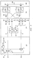
- Latches are often used to control output drivers in digital circuit systems. In some instances it is desirable to enable and disable the output driver. For example, the output driver may be disabled (placed into an open state) so that another logic device may drive the same line that the output driver is connected to. Previously, latches were enabled and disabled using a logic gate placed between the latch and the output driver as shown in Figure 1.
- Latch controlled output driver circuit 70 includes an input circuit 71 , a latch circuit 72 , an enable/disable circuit 74 , and an output driver circuit 76 .
- Input circuit 71 is constructed from pass gates G1 and G2 and inverter I1 ; latch circuit 72 is constructed from inverters I2 - I5 .
- Enable/disable circuit 74 is constructed from NAND gates A1 and A2 and inverters I6 and I7 , and output driver circuit 76 includes transistors T1 and T2 .
- Transistor T1 is a pull-up transistor and transistor T2 is a pull-down transistor in the output driver portion of this circuit.
- Transistors T1 and T2 are n-channel metal-oxide field effect transistors (MOSFETs).
- MOSFETs metal-oxide field effect transistors
- the drain of transistor T1 is connected to power supply voltage VCC
- the source of transistor T2 is connected to power supply voltage VSS.
- power supply voltage VCC is at a higher voltage than power supply voltage VSS.
- Signals are input into latch controlled output driver circuit 70 at inputs GDT and GDC.
- the gate of transistor T1 is controlled by a signal entering the latch controlled output driver at input GDT; the gate of transistor T2 is controlled by a signal entering the latch controlled output driver 70 at input GDC.
- Pass gates G1 and G2 control the flow of the signal from inputs GDT and GDC to output driver circuit 76 .
- Pass gates G1 and G2 are controlled by a clock signal, CLK applied to point 80 and a complement clock signal, /CLK, which is generated by passing the clock signal through inverter I1 .
- inverters I2 and I3 are cross-coupled; inverters I4 and I5 are cross-coupled.
- pass gates G1 and G2 are turned off, inverters I2 - I5 provide the latching mechanism to provide a continuous signal to the gates of transistor T1 and T2 when output driver circuit 76 is enabled by enable/disable circuit 74 .
- NAND gates A1 and A2 in enable/disable circuit 74 are employed to enable and disable output driver circuit 76 .
- Signals from input points GDT and GDC are allowed to travel through NAND gates A1 and A2 to the gates of transistors T1 and T2 when the signal at inputs OE are a logic one.
- the latch controlled output circuit 70 is disabled, both transistors are off, and the output of output driver circuit 76 is a high Z.
- the present invention provides a latch controlled output driver that contains an output driver circuit including a pull-up transistor and a pull-down transistor connected in series. An output is located at a node between the two transistors. The gate of each transistor has a latch connected to it to latch data. A control circuit is connected to the inputs of the latches and connects the data inputs to the latches in an enabled state. When the control circuit places the latch controlled output driver in a disabled state, the latches are forced to a value which turns off both output transistors. Data is stored in a data circuit before the latches are driven to disable the latch controlled output driver. The data is restored to the latches from the data circuit when the latch controlled output driver circuit returns to an enabled state.
- a latch controlled output driver comprising an output driver circuit including a pull-up transistor and a pull-down transistor connected in series, wherein the pull-up transistor has a source/drain connected to a first power supply voltage and a source/drain connected to a source/drain of the pull-down transistor and the pull-down transistor has a source/drain connected to a second power supply voltage, a driver output located between the pull-up and pull-down transistors, a first latch circuit having an input and an output, wherein the output of the first latch circuit is connected to a gate of the pull-up transistor, a second latch circuit having an input and an output, wherein the output of the second latch circuit is connected to a gate of the pull-down transistor, a control circuit connected to the first and second latches, wherein the control circuit may selectively set the first and second latches to a first and second preselected state in response to a control signal, wherein the pull-up and pull-down transistors are turned off
- the control circuit may comprise a first disable circuit connected to the first latch, wherein the first latch may be set to a first preselected state by the first disable circuit, and a second disable cicuit connected to the second latch, wherein the second latch may be set to a second preselected state by the second disable circuit.
- Each disable circuit may include three transistors connected in series, a first transistor having a first source/drain connected to the first power supply voltage and a second source/drain connected to input ofa latch, wherein the first transistor is turned on and off by a signal and wherein the latch controlled output driver is disabled when the first transistor is turned on and the latch controlled output driver is enabled when the first transistor is turned off, a second transistor having a first source/drain connected to the input of a latch, wherein the second transistor is turned on and off a second signal, and a third transistor having a first source/drain connected to a second source/drain of the second transistor and a second source/drain connected to the second power supply voltage, wherein the third transistor is controlled by a data signal.
- the latch controlled output driver may further comprise a data circuit connected to a gate of the third transistor in the first and second latches, wherein the data circuit stores data and sends the data to the first and second latches when the latch controller output driver is enabled after being disabled and the second transistor in each of the disable circuits is turned on.
- the data circuit may selectively turn on the third transistors in the disable circuits to restore the state of the first and second latches.
- the second signal may be a pulse that turns on the second transistor in the disable circuits for a selected period of time, wherein the state of the first and second latches are restored during the selected period of time.
- the selected period of time may begin after the latch controlled output driver is enabled after being disabled.
- the latch controlled output driver may further comprise a first gate having an output connected to the input of the first latch and a second gate having an output conneted to the input of the second latch, wherein the first and second gates send data to the first and second latches, wherein the pulse is generated only if first and second gates are turned off.
- the latch controlled output driver may further comprise a NOR gate having an output, a first input, and a second input, the outputbeing connected to the gates of the second transistors in the first and second latches, an inverter having an input and an output, a NAND gate having an output, a first input, and a second input, the output being connected to the first input of the NOR gate and the first input being connected to an output of an inverter, and a connection point connected to the second input of the NOR gate and the input of the inverter, wherein the output of the NOR gate generates a pulse in response to a logic one applied to the second input of the NAND gate and a logic zero applied to the connection point.
- the first transistor may be a p-channel field effect transistor
- the second and third transistors may be n-channel field effect transistors.
- Memory array 100 (also just called a "memory”) is subdivided into eight memory groups: 0 - 7 . Each memory group contains a memory block 102a , a memory block 102b , and an input/output (I/O) block 104a . I/O block 104a is interposed between the two memory blocks 102a and 102b .
- Data bus latch block 106 is connected to the I/O blocks 104a of memory groups 0 - 7 via a data bus 108 .
- Data bus latch block 106 also has an output bus 109 .
- Data bus latch block 106 includes latch controlled output drivers, as will now be described.
- Latch controlled output driver 198 contains input circuit 200 , enable/disable circuit 202 , latch circuit 204 , and output driver circuit 206.
- Input circuit 200 includes pass gates G1 and G2 , inverters I1 and I6 , and NAND gate N3 .
- Pass gates G1 and G2 pass data from input points GDT and GDC in input circuit 200 to the rest of the circuits.
- input points GDT and GDC are connected to buses that are precharged high between clock cycles generated by the clock signal. Afterward, one of the input points, GDT or GDC, goes low when data is read.
- Pass gates G1 and G2 are controlled by CLK and /CLK signals originating from NAND gate N3 and inverter I1 .
- the clock signal is generated by a signal applied to input GDL.
- Pass gates G1 and G2 may be disabled by a disable signal (a logic one) being applied to point OD and traveling through inverter I6 into NAND gate N3 .
- Enable/disable circuit 202 includes an SR latch L1 formed by NAND gates N1 and N2 .
- SR latch L1 stores data input at input points GDT and GDC. For example, if GDT is a logic one and GDC is a logic zero, point LD is a logic zero and point /LD is a logic one in SR latch L1 .
- Enable/disable circuit 204 also contains transistors D1 - D6 .
- Transistors D1 and D4 are p-channel MOSFETs, while transistors D2 , D3 , D5 , and D6 are n-channel MOSFETs.
- Transistors D1 and D4 have sources connected to power supply voltage VCC, while transistors D3 and D6 have sources connected to power supply voltage VSS. Transistors D1 - D3 are connected in series and transistors D4 - D6 also are connected in series. The gates of transistors D1 and D4 are controlled by a complementary disable signal being applied to point /OD, while the gates of transistors D2 and D5 are controlled by signals applied to points OE. Finally, the gates of transistors D3 and D6 are controlled by the output of SR latch L1 formed by NAND gates N1 and N2 . NAND gate N1 produces a signal LD, while NAND gate N2 produces a signal /LD.
- Latch circuit 204 includes latches L2 and L3 formed by cross-coupled inverters I2 and I3 , and I4 and I5 .
- Transistors P1 and P2 are p-channel MOSFETs employed to provide stability to latch controlled output driver circuit driver 198 .
- Output driver circuit 206 includes transistors T1 and T2 .
- Transistor T1 is a pull-up transistor, while transistor T2 is a pull-down transistor.
- the signals applied to input points GDT and GDC result in an output signal at output point 208 when latch controlled output circuit 198 is enabled.
- output point 208 is disabled.
- This disable signal (a logic one for point OD and a logic zero for point /OD) causes pass gates G1 and G2 to be disabled regardless of the signal at point GDL.
- transistors D1 and D4 are turned on, which pulls points DT and DC high regardless of the signal generated by latches L2 and L3 .
- Inverters I3 and I5 are weak in accordance with a preferred embodiment of the present invention. Thus, the state of points DT and DC are easily changed in response to transistors D1 - D6 .
- FIG. 4 a schematic diagram of a circuit for providing an end of disable pulse (EOD) is depicted.
- the circuit includes a NOR gate N4 that has an input connected to the output of a NAND gate N5 .
- the other input of NOR gate N4 is connected point OD.
- NAND gate N5 has an input for GDL C , which prevents an EOD pulse from being generated when point GDL C is a logic zero.
- the signal applied to point GDL C is always the complement of the signal applied to point GDL.
- NAND gate N5 also has an input connected to a series of inverters I7 and I8 .
- This circuit provides a high going pulse at output EOD when point OD goes to a logic zero.
- Inverters I1 and I7 provide delays to set the width of the EOD pulse generated at output OE. Different numbers or inverters or different types of inverters may be employed to alter the width or duration of the EOD pulse.
- a logic zero signal is applied to point OD and a logic one signal is applied to points /OD to enable latch controlled output driver circuit 198 .
- transistors D1 and D4 are turned off and a EOD pulse is generated (if GDL C is high) to restore the latch state stored in latch L1 to latches L2 and L3 in latch circuit 204 .
- Such a restoration of the latch state to latches L2 and L3 may be necessary because by this time points GDC and GDT may have been precharged high, eliminating the previous data. This situation is possible because the signal at point OD is asynchronous to the signal at GDL (clock signal).
- the EOD pulse is applied to points OE, which control transistors D2 and D5 . When these two transistors, D2 and D5 , are turned on, points DT and DC are restored to the states stored in SR latch L1 .
- the state of latch L1 causes transistor D3 to stay off in response to signal at point, LD leaving point DT at a logic one.
- transistor D6 is turned on pulling point DC down to a logic zero.
- the data originally input at points GDT and GDC (a logic one and a logic zero) are returned to their original states in latches L2 and L3 .
- latch controlled output driver circuit 198 When latch controlled output driver circuit 198 is enabled, the signal at point OD is a logic zero and the signal at point /OD is a logic one. A logic one at point /OD results in transistors D1 and D6 being turned off so that the restored data is not changed.
- transistors D2 and D5 are turned off, however, the data already has been restored from SR latch L1 to latches L2 and L3 .
- GDL C is a logic zero
- the EOD pulse is eliminated so that data from latch L1 at output point 208 is not written at points DT and DC .
- GDL c is set equal to zero when the pass gates are being turned on. This avoids conflict with incoming new data at points GDC and GDT.
- the EOD pulse is eliminated so that data stored in SR latch L1 is not output at output point 208 and allows for the incoming new data to be output at output point 208 .
- the signal at point OD is a logic one
- the signal at point /OD is a logic zero.
- pass gates G1 and G2 are turned off and transistors D1 and D4 are turned on pulling both points DT and DC high causing an open or Hi-Z state at output point 208 .
- transistors D2 and D5 are turned off, preventing any change in points DT and DC by transistors D3 and D6 .
- other logic devices may drive the line to which output point 208 is connected.
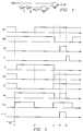
- FIG. 5 is a timing chart of various input an output conditions for a latch controlled output driver according to the present invention.
- GDT and GDC are precharged during time p1 .
- GDT drops to a logic zero while GDC remains high, a logic one.
- the CLK signal at point GDL turns on or opens pass gates G1 and G2 setting points DT and DC , which in turn sets the states of latches L2 and L3 to a logic zero and a logic one respectively.
- latch L1 stores data from GDT and GDC as complement signals as seen at points LD and /LD.
- points GDT and GDC are again precharged high.
- Points DT and DC remain a logic zero and logic one.
- GDT remains a logic one, and GDC drops to a logic zero.
- the CLK signal activates pass gates G1 and G2 and sets points DT and DC to a logic one and a logic zero, setting latch L2 to a logic one and latch L3 to a logic zero.
- a disable signal is sent to the latch controlled output driver circuit 198 at point OD, disabling latches L2 and L3 .
- Point DC is pulled up to a logic one causing the output point 208 to have a Hi-Z impedance as can be seen by the graph of Hi-Z in Figure 5 .
- the disable signal at OD is ended and a EOD signal is generated at points OE, resulting in the data stored in the latch L1 being restored to latch L2 and L3 as can be seen by points DT and DC being restored to a logic one and a logic zero respectively.
- the latch controlled output driver circuit 198 may be efficiently enabled and disabled since additional logic gates between latch circuit 204 and output driver circuit 206 may be eliminated. Latches L1 and L2 may be restored to the previous data states using the present invention upon reenabling the latch controlled output driver. Additionally, the elimination of the NAND gates shown in the prior art provide a faster response in latch controlled driver circuit 198 . Employing the present latch controlled driver circuit in a memory can speed up the response of the memory and other circuits requiring latch controlled output driver circuits. Although the present invention is depicted using MOS technology, other types of technology and transistors may be used in accordance with a preferred embodiment of the present invention.
- latches and inverters may be replaced with NAND gates instead, with the other input being from point Dc for the NAND gate replacing inverter I3 and from point Dt for the NAND gate replacing inverter I5 .
- the depicted embodiment shows the use of pass gates for gating or sending information into the latches.
- Other types of gates or devices known to those skilled the art for gating or providing an interface circuit for controlling data reaching the latches may be used according to the present invention.
Landscapes
- Engineering & Computer Science (AREA)
- Power Engineering (AREA)
- Physics & Mathematics (AREA)
- Computer Hardware Design (AREA)
- Computing Systems (AREA)
- General Engineering & Computer Science (AREA)
- Mathematical Physics (AREA)
- Logic Circuits (AREA)
- Static Random-Access Memory (AREA)
- Electronic Switches (AREA)
- Dram (AREA)
Applications Claiming Priority (2)
| Application Number | Priority Date | Filing Date | Title |
|---|---|---|---|
| US08/129,257 US5396108A (en) | 1993-09-30 | 1993-09-30 | Latch controlled output driver |
| US129257 | 1993-09-30 |
Publications (3)
| Publication Number | Publication Date |
|---|---|
| EP0647028A2 true EP0647028A2 (de) | 1995-04-05 |
| EP0647028A3 EP0647028A3 (de) | 1996-01-24 |
| EP0647028B1 EP0647028B1 (de) | 2002-03-20 |
Family
ID=22439140
Family Applications (1)
| Application Number | Title | Priority Date | Filing Date |
|---|---|---|---|
| EP94307070A Expired - Lifetime EP0647028B1 (de) | 1993-09-30 | 1994-09-28 | Verriegelungsschaltungsgesteuerter Ausgangstreiber |
Country Status (4)
| Country | Link |
|---|---|
| US (1) | US5396108A (de) |
| EP (1) | EP0647028B1 (de) |
| JP (1) | JP3526921B2 (de) |
| DE (1) | DE69430165T2 (de) |
Cited By (1)
| Publication number | Priority date | Publication date | Assignee | Title |
|---|---|---|---|---|
| EP0696851A1 (de) * | 1994-07-28 | 1996-02-14 | International Business Machines Corporation | Transparenter Hochleistungs-Latch kompatibel mit dynamischen Logikschaltungen |
Families Citing this family (22)
| Publication number | Priority date | Publication date | Assignee | Title |
|---|---|---|---|---|
| TW294861B (de) * | 1992-02-21 | 1997-01-01 | Siemens Ag | |
| US5619466A (en) * | 1996-01-19 | 1997-04-08 | Sgs-Thomson Microelectronics, Inc. | Low-power read circuit and method for controlling a sense amplifier |
| US5745432A (en) * | 1996-01-19 | 1998-04-28 | Sgs-Thomson Microelectronics, Inc. | Write driver having a test function |
| US5883838A (en) * | 1996-01-19 | 1999-03-16 | Stmicroelectronics, Inc. | Device and method for driving a conductive path with a signal |
| JPH09231770A (ja) * | 1996-01-19 | 1997-09-05 | Sgs Thomson Microelectron Inc | メモリセルへの書込を終了させる回路及び方法 |
| US5845059A (en) * | 1996-01-19 | 1998-12-01 | Stmicroelectronics, Inc. | Data-input device for generating test signals on bit and bit-complement lines |
| US5802004A (en) * | 1996-01-19 | 1998-09-01 | Sgs-Thomson Microelectronics, Inc. | Clocked sense amplifier with wordline tracking |
| JPH09282886A (ja) * | 1996-01-19 | 1997-10-31 | Sgs Thomson Microelectron Inc | メモリセルへの書込の開始をトラッキングする回路及び方法 |
| US5864696A (en) * | 1996-01-19 | 1999-01-26 | Stmicroelectronics, Inc. | Circuit and method for setting the time duration of a write to a memory cell |
| US5691950A (en) * | 1996-01-19 | 1997-11-25 | Sgs-Thomson Microelectronics, Inc. | Device and method for isolating bit lines from a data line |
| US5848018A (en) * | 1996-01-19 | 1998-12-08 | Stmicroelectronics, Inc. | Memory-row selector having a test function |
| US5777496A (en) * | 1996-03-27 | 1998-07-07 | Aeg Schneider Automation, Inc. | Circuit for preventing more than one transistor from conducting |
| US5751178A (en) * | 1996-12-05 | 1998-05-12 | Motorola, Inc. | Apparatus and method for shifting signal levels |
| US5864244A (en) * | 1997-05-09 | 1999-01-26 | Kaplinsky; Cecil H. | Tristate buffer circuit with transparent latching capability |
| JP4088466B2 (ja) * | 2002-03-19 | 2008-05-21 | 三菱電機株式会社 | パワーデバイスの駆動回路 |
| US6995598B2 (en) * | 2003-02-13 | 2006-02-07 | Texas Instruments Incorporated | Level shifter circuit including a set/reset circuit |
| US6828838B1 (en) * | 2003-05-30 | 2004-12-07 | Intel Corporation | Vectored flip-flops and latches with embedded output-merge logic and shared clock drivers |
| JP4014048B2 (ja) * | 2004-06-02 | 2007-11-28 | ローム株式会社 | コイル負荷駆動出力回路 |
| US8030960B2 (en) * | 2008-12-29 | 2011-10-04 | Oracle America, Inc. | Converting dynamic repeaters to conventional repeaters |
| US8063673B2 (en) * | 2008-12-29 | 2011-11-22 | Oracle America, Inc. | Transit state element |
| US9647456B2 (en) * | 2014-03-13 | 2017-05-09 | Nxp B.V. | Power management circuit and a method for operating a power management circuit |
| US9570158B1 (en) * | 2016-05-04 | 2017-02-14 | Qualcomm Incorporated | Output latch for accelerated memory access |
Family Cites Families (5)
| Publication number | Priority date | Publication date | Assignee | Title |
|---|---|---|---|---|
| JPS6335009A (ja) * | 1986-07-30 | 1988-02-15 | Toshiba Corp | 半導体回路 |
| JPH073945B2 (ja) * | 1988-06-27 | 1995-01-18 | 日本電気株式会社 | Cmos出力回路 |
| JPH02226589A (ja) * | 1989-02-27 | 1990-09-10 | Nec Corp | 半導体記憶装置 |
| JPH02243015A (ja) * | 1989-03-15 | 1990-09-27 | Nec Corp | 制御回路 |
| US5001369A (en) * | 1990-07-02 | 1991-03-19 | Micron Technology, Inc. | Low noise output buffer circuit |
-
1993
- 1993-09-30 US US08/129,257 patent/US5396108A/en not_active Expired - Lifetime
-
1994
- 1994-09-28 EP EP94307070A patent/EP0647028B1/de not_active Expired - Lifetime
- 1994-09-28 DE DE69430165T patent/DE69430165T2/de not_active Expired - Fee Related
- 1994-09-30 JP JP23620794A patent/JP3526921B2/ja not_active Expired - Fee Related
Non-Patent Citations (1)
| Title |
|---|
| None |
Cited By (1)
| Publication number | Priority date | Publication date | Assignee | Title |
|---|---|---|---|---|
| EP0696851A1 (de) * | 1994-07-28 | 1996-02-14 | International Business Machines Corporation | Transparenter Hochleistungs-Latch kompatibel mit dynamischen Logikschaltungen |
Also Published As
| Publication number | Publication date |
|---|---|
| US5396108A (en) | 1995-03-07 |
| DE69430165T2 (de) | 2002-08-22 |
| EP0647028A3 (de) | 1996-01-24 |
| JPH07170159A (ja) | 1995-07-04 |
| DE69430165D1 (de) | 2002-04-25 |
| JP3526921B2 (ja) | 2004-05-17 |
| EP0647028B1 (de) | 2002-03-20 |
Similar Documents
| Publication | Publication Date | Title |
|---|---|---|
| EP0647028B1 (de) | Verriegelungsschaltungsgesteuerter Ausgangstreiber | |
| US5894238A (en) | Output buffer with static and transient pull-up and pull-down drivers | |
| US6016066A (en) | Method and apparatus for glitch protection for input buffers in a source-synchronous environment | |
| EP0632594B1 (de) | Verriegelungsgesteuerter Ausgangstreiber | |
| US6310491B1 (en) | Sequential logic circuit with active and sleep modes | |
| US5949721A (en) | Data output related circuit which is suitable for semiconductor memory device for high -speed operation | |
| KR960006911B1 (ko) | 데이타 출력버퍼 | |
| US5206545A (en) | Method and apparatus for providing output contention relief for digital buffers | |
| US5489859A (en) | CMOS output circuit with high speed high impedance mode | |
| US5739701A (en) | Input/output buffer circuit having reduced power consumption | |
| EP0174266B1 (de) | CMOS-Ausgangspuffer | |
| JPH08279742A (ja) | プログラム可能な電流駆動出力バッファおよび出力バッファのための駆動電流出力を選択する方法 | |
| US7449924B2 (en) | Latch-based serial port output buffer | |
| EP0202582B1 (de) | NMOS-Datenspeicherzelle und Schieberegister | |
| JP2805466B2 (ja) | メモリのアドレス遷移検出回路 | |
| US6411553B1 (en) | Single ended data bus equilibration scheme | |
| US5394363A (en) | Pulse write driver circuit | |
| US6366520B1 (en) | Method and system for controlling the slew rate of signals generated by open drain driver circuits | |
| US5296758A (en) | Output buffer with ground bounce compensation | |
| JP2000341109A (ja) | ロジックインターフェース回路及び半導体メモリ装置 | |
| US6292405B1 (en) | Data output buffer with precharge | |
| KR0179816B1 (ko) | 출력버퍼 회로 | |
| EP0614293B1 (de) | Multiplexer | |
| KR100205094B1 (ko) | 반도체 소자의 출력버퍼 회로 | |
| KR950002085B1 (ko) | 개선된 래치회로를 갖는 데이타 출력버퍼 |
Legal Events
| Date | Code | Title | Description |
|---|---|---|---|
| PUAI | Public reference made under article 153(3) epc to a published international application that has entered the european phase |
Free format text: ORIGINAL CODE: 0009012 |
|
| AK | Designated contracting states |
Kind code of ref document: A2 Designated state(s): DE FR GB IT |
|
| PUAL | Search report despatched |
Free format text: ORIGINAL CODE: 0009013 |
|
| AK | Designated contracting states |
Kind code of ref document: A3 Designated state(s): DE FR GB IT |
|
| 17P | Request for examination filed |
Effective date: 19960706 |
|
| 17Q | First examination report despatched |
Effective date: 19961210 |
|
| RAP3 | Party data changed (applicant data changed or rights of an application transferred) |
Owner name: STMICROELECTRONICS, INC. |
|
| GRAG | Despatch of communication of intention to grant |
Free format text: ORIGINAL CODE: EPIDOS AGRA |
|
| GRAG | Despatch of communication of intention to grant |
Free format text: ORIGINAL CODE: EPIDOS AGRA |
|
| GRAH | Despatch of communication of intention to grant a patent |
Free format text: ORIGINAL CODE: EPIDOS IGRA |
|
| GRAH | Despatch of communication of intention to grant a patent |
Free format text: ORIGINAL CODE: EPIDOS IGRA |
|
| REG | Reference to a national code |
Ref country code: GB Ref legal event code: IF02 |
|
| GRAA | (expected) grant |
Free format text: ORIGINAL CODE: 0009210 |
|
| AK | Designated contracting states |
Kind code of ref document: B1 Designated state(s): DE FR GB IT |
|
| PG25 | Lapsed in a contracting state [announced via postgrant information from national office to epo] |
Ref country code: IT Free format text: LAPSE BECAUSE OF FAILURE TO SUBMIT A TRANSLATION OF THE DESCRIPTION OR TO PAY THE FEE WITHIN THE PRESCRIBED TIME-LIMIT;WARNING: LAPSES OF ITALIAN PATENTS WITH EFFECTIVE DATE BEFORE 2007 MAY HAVE OCCURRED AT ANY TIME BEFORE 2007. THE CORRECT EFFECTIVE DATE MAY BE DIFFERENT FROM THE ONE RECORDED. Effective date: 20020320 |
|
| REF | Corresponds to: |
Ref document number: 69430165 Country of ref document: DE Date of ref document: 20020425 |
|
| ET | Fr: translation filed | ||
| PLBE | No opposition filed within time limit |
Free format text: ORIGINAL CODE: 0009261 |
|
| STAA | Information on the status of an ep patent application or granted ep patent |
Free format text: STATUS: NO OPPOSITION FILED WITHIN TIME LIMIT |
|
| 26N | No opposition filed |
Effective date: 20021223 |
|
| PGFP | Annual fee paid to national office [announced via postgrant information from national office to epo] |
Ref country code: DE Payment date: 20031009 Year of fee payment: 10 |
|
| PGFP | Annual fee paid to national office [announced via postgrant information from national office to epo] |
Ref country code: FR Payment date: 20040908 Year of fee payment: 11 |
|
| PGFP | Annual fee paid to national office [announced via postgrant information from national office to epo] |
Ref country code: GB Payment date: 20040922 Year of fee payment: 11 |
|
| PG25 | Lapsed in a contracting state [announced via postgrant information from national office to epo] |
Ref country code: DE Free format text: LAPSE BECAUSE OF NON-PAYMENT OF DUE FEES Effective date: 20050401 |
|
| PG25 | Lapsed in a contracting state [announced via postgrant information from national office to epo] |
Ref country code: GB Free format text: LAPSE BECAUSE OF NON-PAYMENT OF DUE FEES Effective date: 20050928 |
|
| GBPC | Gb: european patent ceased through non-payment of renewal fee |
Effective date: 20050928 |
|
| PG25 | Lapsed in a contracting state [announced via postgrant information from national office to epo] |
Ref country code: FR Free format text: LAPSE BECAUSE OF NON-PAYMENT OF DUE FEES Effective date: 20060531 |
|
| REG | Reference to a national code |
Ref country code: FR Ref legal event code: ST Effective date: 20060531 |