EP0647933A1 - Punktaktgeber für Flüssigkristallenzeigegerät - Google Patents
Punktaktgeber für Flüssigkristallenzeigegerät Download PDFInfo
- Publication number
- EP0647933A1 EP0647933A1 EP94307146A EP94307146A EP0647933A1 EP 0647933 A1 EP0647933 A1 EP 0647933A1 EP 94307146 A EP94307146 A EP 94307146A EP 94307146 A EP94307146 A EP 94307146A EP 0647933 A1 EP0647933 A1 EP 0647933A1
- Authority
- EP
- European Patent Office
- Prior art keywords
- dot clock
- signal
- liquid crystal
- crystal display
- period
- Prior art date
- Legal status (The legal status is an assumption and is not a legal conclusion. Google has not performed a legal analysis and makes no representation as to the accuracy of the status listed.)
- Ceased
Links
Images


Classifications
-
- G—PHYSICS
- G09—EDUCATION; CRYPTOGRAPHY; DISPLAY; ADVERTISING; SEALS
- G09G—ARRANGEMENTS OR CIRCUITS FOR CONTROL OF INDICATING DEVICES USING STATIC MEANS TO PRESENT VARIABLE INFORMATION
- G09G5/00—Control arrangements or circuits for visual indicators common to cathode-ray tube indicators and other visual indicators
- G09G5/003—Details of a display terminal, the details relating to the control arrangement of the display terminal and to the interfaces thereto
- G09G5/006—Details of the interface to the display terminal
- G09G5/008—Clock recovery
-
- H—ELECTRICITY
- H03—ELECTRONIC CIRCUITRY
- H03L—AUTOMATIC CONTROL, STARTING, SYNCHRONISATION OR STABILISATION OF GENERATORS OF ELECTRONIC OSCILLATIONS OR PULSES
- H03L7/00—Automatic control of frequency or phase; Synchronisation
- H03L7/06—Automatic control of frequency or phase; Synchronisation using a reference signal applied to a frequency- or phase-locked loop
- H03L7/07—Automatic control of frequency or phase; Synchronisation using a reference signal applied to a frequency- or phase-locked loop using several loops, e.g. for redundant clock signal generation
-
- H—ELECTRICITY
- H03—ELECTRONIC CIRCUITRY
- H03L—AUTOMATIC CONTROL, STARTING, SYNCHRONISATION OR STABILISATION OF GENERATORS OF ELECTRONIC OSCILLATIONS OR PULSES
- H03L7/00—Automatic control of frequency or phase; Synchronisation
- H03L7/06—Automatic control of frequency or phase; Synchronisation using a reference signal applied to a frequency- or phase-locked loop
- H03L7/16—Indirect frequency synthesis, i.e. generating a desired one of a number of predetermined frequencies using a frequency- or phase-locked loop
- H03L7/18—Indirect frequency synthesis, i.e. generating a desired one of a number of predetermined frequencies using a frequency- or phase-locked loop using a frequency divider or counter in the loop
-
- H—ELECTRICITY
- H04—ELECTRIC COMMUNICATION TECHNIQUE
- H04N—PICTORIAL COMMUNICATION, e.g. TELEVISION
- H04N5/00—Details of television systems
- H04N5/04—Synchronising
- H04N5/12—Devices in which the synchronising signals are only operative if a phase difference occurs between synchronising and synchronised scanning devices, e.g. flywheel synchronising
- H04N5/126—Devices in which the synchronising signals are only operative if a phase difference occurs between synchronising and synchronised scanning devices, e.g. flywheel synchronising whereby the synchronisation signal indirectly commands a frequency generator
Definitions
- the present invention generally relates to a dot clock generator for a liquid crystal display device, and more particularly to such generator which can generate a dot clock with less skew from a sync signal.
- the CRT (cathode ray tube) has been widely used as a monitor of a personal computer, and the interface between the personal computer and CRT is made unique to the CRT. Specifically, R, G, and B analog signals, and vertical and horizontal sync signals are generated in the personal computer unit and provided to the CRT.
- the liquid crystal display device needs to generate an additional dot clock. In other words, the liquid crystal display device needs to receive R, G, and B digital signals for every dot timing (dot clock) to drive the liquid crystal panel based on these signals. Since the personal computer unit outputs only the analog RGB and sync signals to the above CRT interface, it is necessary to generate a dot clock from the sync signals and, according to the timing of this clock, convert the analog RGB signals to digital RGB signals by the A/D conversion.
- a phase locked loop (PLL) circuit shown in Fig. 1 may be used to generate a dot clock from a sync signal, i.e. horizontal sync signal.
- phase comparator 11 is supplied with the horizontal sync signal and the output of frequency divider 12.
- the comparison outputs (positive and negative) of phase comparator 11 is inputted to voltage controlled oscillator (VCO) 15 via filter 13 and capacitor 14.
- VCO voltage controlled oscillator
- the output of VCO 15 is given as a dot clock and fed back to frequency divider 12. Assuming that frequency divider 12 has a division ratio of 1/N, the dot clock to be outputted will have a frequency of N times the horizontal sync signal.
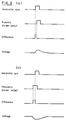
- the noise from frequency divider 12 is superimposed on the voltage across capacitor 14, leading to a difficulty in generating a stable dot clock necessary for the liquid crystal display. If the phase of frequency divider 12 is delayed with respect to the horizontal sync signal, i.e. if the clock frequency is too low, the voltage across capacitor 14 would increase to increase the clock frequency for compensation, as shown in Fig. 2(a). On the other hand, if the phase of frequency divider 12 is advanced with respect to the horizontal sync signal, i.e. if the clock frequency is too high, the voltage across capacitor 14 would decrease to lower the clock frequency for compensation, as shown in Fig. 2(b). However, the voltage across capacitor 14 is subject to the noise from frequency divider 12 which skews the clock frequency to thereby disturb the screen.
- the present invention has an object to provide a PLL mechanism which is capable of generating the dot clock with less skew from the horizontal sync signal.
- the PLL is divided into three functional parts in accordance with the present invention.
- the first part is a means for obtaining a particular frequency.
- This means is designed such that a latch type DAC (digital/analog converter) supplies a voltage to a VCO.
- the horizontal sync signal is estimated from the dot clock finally generated, and the value of the DAC is increased or decreased according to the difference between the estimated horizontal sync signal and the actual horizontal sync signal. The compensation by this increase or decrease is made at, for example, the vertical sync timing.
- the second part is a synchronization means.
- a signal corresponding to the phase error between the actual horizontal sync signal and dot clock is added to the signal from DAC to control the phase of the dot clock.
- the third part is a PLL means for generating a dot clock according to the signal having the particular frequency mentioned above.
- a dot clock generator for a liquid crystal display device comprising a reference voltage generator means including a latch type digital/analog converter; a voltage controlled oscillator means which oscillates according to a reference voltage from said reference voltage generator means to produce a reference clock; a phase locked loop circuit means for producing a dot clock according to said reference clock; means for producing a horizontal period signal from said dot clock; means for receiving an external horizontal period signal; means for detecting a phase error between said horizontal period signal generated from said dot clock and said horizontal period signal received externally; means for adjusting the latched data of said analog/digital converter according to said phase error in a first period which is longer than said horizontal period; and means for adjusting said reference voltage to be inputted to said voltage controlled oscillator according to said phase error in a second period which is shorter than said first period.
- the present invention also provides a liquid crystal display device comprising: a liquid crystal display element; a display control means for generating a digital video signal based on analog video and sync signals and providing said digital video signal to said liquid crystal display element; a dot clock generator according to any of the preceding claims wherein said external horizontal period signal is derived from said sync signal; means for providing said dot clock to said display control means.
- Fig. 1 shows a block diagram illustrating a conventional configuration.
- Fig. 2 shows a waveform illustrating the problem of the conventional configuration.
- Fig. 3 shows a block diagram illustrating an embodiment of the present invention.
- Fig. 4 shows a block diagram illustrating the detailed arrangement of the embodiment shown in Fig. 3.
- Fig. 3 shows the overall configuration of this embodiment in which a vertical sync signal, horizontal sync signal, and R, G, and B video signals are supplied from a personal computer (processing unit) to terminals 21 to 25, respectively. These signals are then supplied to LCD controller 26 which generate R, G, and B digital video signals and other control signals for LCD module 27.
- a dot clock is also supplied from dot clock generator 28 to LCD controller 26.
- Dot clock generator 28 generates a dot clock, which is variable in a range from 50 to 80 MHz, from the vertical and horizontal sync signals. As described above, the dot clock is used to generate the digital video signal for each dot or pixel.
- Dot clock generator 28 includes reference voltage generator 29 and voltage controlled oscillator 30 for a reference clock.
- Voltage controlled oscillator 30 is provided with a ceramic resonator to generate a reference clock having a 2 MHz center frequency in accordance with the reference voltage from reference voltage generator 29.
- This reference clock is applied to internal PLL circuit 31 which generates, for example, a 50 to 80 MHz dot clock according to the division ratio of programmed frequency divider 32.
- This dot clock is supplied to LCD controller 26 as well as horizontal sync signal generator 33 which counts the dot clock according to its frequency and generates a horizontal sync signal.
- the generated horizontal sync signal is supplied to horizontal sync signal comparator 34.
- the comparator 34 also receives a horizontal sync signal from terminal 22 via horizontal sync signal skew generator 35 and compares the phases of both signals.
- a phase error signal is supplied to voltage controlled oscillator 30 and reference voltage adjuster 36.
- Voltage controlled oscillator 30 receives the error signal in a horizontal frequency to ensure that the reference clock is in phase with the horizontal sync signal.
- Reference voltage adjuster 36 receives the error signal in a vertical period to control reference voltage generator 29 to ensure that the reference clock is aligned with the actual horizontal sync signal in the vertical period.
- Fig. 4 shows the details of the major portion of the embodiment shown in Fig. 3.
- reference voltage generator 29 comprises a latch type digital/analog converter (DAC) and supplies the reference voltage to voltage controlled oscillator 30 via resistors.
- Reference voltage adjuster 36 increments or decrements in the vertical period the latched data of the DAC by a predetermined number, e.g. 1, according to the positive or negative error signal from horizontal sync signal comparator 34 to correct the reference voltage.
- the error signal is added to the reference voltage in the horizontal period via serial circuits 41 and 42 each consisting of a resistor and a capacitor to ensure that voltage controlled oscillator 30 is in phase with the horizontal signal.
- Internal PLL 31 comprises 1/8 frequency divider 37, phase comparator 38, low-pass filter 39, and voltage controlled oscillator 40.
- a signal of approximately 250 KHz from frequency divider 37 is compared by phase comparator 38 with the signal from programmed frequency divider 32 to allow the frequency or phase of the dot clock to be corrected in an interval of approximately 250 KHz.
- the reference clock can be stabilized even with jitters of the horizontal sync signal since the reference voltage is set up in the vertical period. Oscillation can also be stabilized since it is not necessary to alter the reference clock frequency in a wide range and voltage controlled oscillator 30 using the resonator may be used.
- the input voltage of voltage controlled oscillator 30 is finely adjusted in the horizontal period in response to the phase error between the horizontal sync signal and dot clock (horizontal sync signal generated from the dot clock), the resulting dot clock is precisely locked to the vertical sync signal.
- Internal PLL 31 only divides a stable reference voltage, and the dot clock skew caused by disturbance to this internal PLL 31 is extremely small. Especially, since the comparison period (250 KHz in Fig. 4) of phase comparator 38 in internal PLL 31 is short, the dot clock skew can be corrected with this short period. This not only ensures skew reduction, but also solves a problem of skew accumulated for a long period (horizontal period when the phase error is corrected in the horizontal period). Moreover, although compensation by the feedback of PLL requires several error detections, compensation in this embodiment is completed in a period two or three times of 1/250 KHz (4 microseconds), thus being considerably faster in comparison with two or three times the horizontal period (31.5 microseconds).
- the dot clock skew which impairs the screen can be reduced.
Landscapes
- Engineering & Computer Science (AREA)
- Physics & Mathematics (AREA)
- Computer Hardware Design (AREA)
- General Physics & Mathematics (AREA)
- Theoretical Computer Science (AREA)
- Multimedia (AREA)
- Signal Processing (AREA)
- Liquid Crystal Display Device Control (AREA)
- Synchronizing For Television (AREA)
- Transforming Electric Information Into Light Information (AREA)
- Liquid Crystal (AREA)
- Control Of Indicators Other Than Cathode Ray Tubes (AREA)
Applications Claiming Priority (2)
| Application Number | Priority Date | Filing Date | Title |
|---|---|---|---|
| JP5245098A JP2537013B2 (ja) | 1993-09-30 | 1993-09-30 | 液晶表示装置用のドット・クロック生成装置 |
| JP245098/93 | 1993-09-30 |
Publications (1)
| Publication Number | Publication Date |
|---|---|
| EP0647933A1 true EP0647933A1 (de) | 1995-04-12 |
Family
ID=17128584
Family Applications (1)
| Application Number | Title | Priority Date | Filing Date |
|---|---|---|---|
| EP94307146A Ceased EP0647933A1 (de) | 1993-09-30 | 1994-09-29 | Punktaktgeber für Flüssigkristallenzeigegerät |
Country Status (3)
| Country | Link |
|---|---|
| US (1) | US5479073A (de) |
| EP (1) | EP0647933A1 (de) |
| JP (1) | JP2537013B2 (de) |
Cited By (3)
| Publication number | Priority date | Publication date | Assignee | Title |
|---|---|---|---|---|
| US6316974B1 (en) | 2000-08-26 | 2001-11-13 | Rgb Systems, Inc. | Method and apparatus for vertically locking input and output signals |
| GB2387012A (en) * | 2000-12-15 | 2003-10-01 | Lg Philips Lcd Co Ltd | Liquid crystal display driving method |
| US7791599B2 (en) | 2000-12-15 | 2010-09-07 | Lg Display Co., Ltd. | Liquid crystal display and driving method thereof |
Families Citing this family (10)
| Publication number | Priority date | Publication date | Assignee | Title |
|---|---|---|---|---|
| JP3109940B2 (ja) * | 1993-04-28 | 2000-11-20 | キヤノン株式会社 | 表示制御装置及び情報処理装置 |
| JP3307750B2 (ja) * | 1993-12-28 | 2002-07-24 | キヤノン株式会社 | 表示制御装置 |
| JPH07199891A (ja) * | 1993-12-28 | 1995-08-04 | Canon Inc | 表示制御装置 |
| JPH0944122A (ja) * | 1995-08-03 | 1997-02-14 | Sharp Corp | 液晶表示システム |
| JP3487119B2 (ja) * | 1996-05-07 | 2004-01-13 | 松下電器産業株式会社 | ドットクロック再生装置 |
| US6693987B1 (en) | 2000-10-05 | 2004-02-17 | Pericom Semiconductor Corp. | Digital-to-analog DAC-driven phase-locked loop PLL with slave PLL's driving DAC reference voltages |
| KR20030027385A (ko) * | 2001-09-28 | 2003-04-07 | 삼성전자주식회사 | 보상 제어 장치 및 방법 |
| US6762634B1 (en) | 2003-08-13 | 2004-07-13 | Pericom Semiconductor Corp. | Dual-loop PLL with DAC offset for frequency shift while maintaining input tracking |
| JP4769431B2 (ja) * | 2004-05-28 | 2011-09-07 | Okiセミコンダクタ株式会社 | ドットクロック同期生成回路 |
| KR100790984B1 (ko) * | 2006-03-03 | 2008-01-02 | 삼성전자주식회사 | Dot 클럭 신호의 주파수에 관계없이 일정한 주파수의시스템 클럭 신호를 생성하는 디스플레이용 구동 집적회로및 시스템 클럭 신호 생성 방법 |
Citations (3)
| Publication number | Priority date | Publication date | Assignee | Title |
|---|---|---|---|---|
| US3769602A (en) * | 1972-08-07 | 1973-10-30 | Rca Corp | Analog phase tracker |
| US4893319A (en) * | 1988-12-19 | 1990-01-09 | Planar Systems, Inc. | Clock regeneration circuit employing digital phase locked loop |
| EP0522181A1 (de) * | 1991-01-29 | 1993-01-13 | Seiko Epson Corporation | Videobildverarbeitungsanlage |
Family Cites Families (5)
| Publication number | Priority date | Publication date | Assignee | Title |
|---|---|---|---|---|
| JPS5324140B2 (de) * | 1973-01-24 | 1978-07-19 | ||
| JPS59208590A (ja) * | 1983-05-11 | 1984-11-26 | シャープ株式会社 | 表示装置の駆動回路 |
| US5019807A (en) * | 1984-07-25 | 1991-05-28 | Staplevision, Inc. | Display screen |
| JP2775941B2 (ja) * | 1989-12-08 | 1998-07-16 | 株式会社日本自動車部品総合研究所 | El素子の駆動装置 |
| JP2770631B2 (ja) * | 1992-01-27 | 1998-07-02 | 日本電気株式会社 | 表示装置 |
-
1993
- 1993-09-30 JP JP5245098A patent/JP2537013B2/ja not_active Expired - Lifetime
-
1994
- 1994-09-29 EP EP94307146A patent/EP0647933A1/de not_active Ceased
- 1994-09-30 US US08/316,310 patent/US5479073A/en not_active Expired - Lifetime
Patent Citations (3)
| Publication number | Priority date | Publication date | Assignee | Title |
|---|---|---|---|---|
| US3769602A (en) * | 1972-08-07 | 1973-10-30 | Rca Corp | Analog phase tracker |
| US4893319A (en) * | 1988-12-19 | 1990-01-09 | Planar Systems, Inc. | Clock regeneration circuit employing digital phase locked loop |
| EP0522181A1 (de) * | 1991-01-29 | 1993-01-13 | Seiko Epson Corporation | Videobildverarbeitungsanlage |
Cited By (7)
| Publication number | Priority date | Publication date | Assignee | Title |
|---|---|---|---|---|
| US6316974B1 (en) | 2000-08-26 | 2001-11-13 | Rgb Systems, Inc. | Method and apparatus for vertically locking input and output signals |
| WO2002019311A1 (en) * | 2000-08-26 | 2002-03-07 | Rgb Systems, Inc. | Method and apparatus for vertically locking input and output video signals |
| US6441658B1 (en) | 2000-08-26 | 2002-08-27 | Rgb Systems, Inc. | Method and apparatus for vertically locking input and output signals |
| GB2387012A (en) * | 2000-12-15 | 2003-10-01 | Lg Philips Lcd Co Ltd | Liquid crystal display driving method |
| GB2387012B (en) * | 2000-12-15 | 2004-07-28 | Lg Philips Lcd Co Ltd | Liquid crystal display and driving method thereof |
| US7791599B2 (en) | 2000-12-15 | 2010-09-07 | Lg Display Co., Ltd. | Liquid crystal display and driving method thereof |
| US8004509B2 (en) | 2000-12-15 | 2011-08-23 | Lg Display Co., Ltd. | Liquid crystal display and driving method thereof |
Also Published As
| Publication number | Publication date |
|---|---|
| US5479073A (en) | 1995-12-26 |
| JPH07110667A (ja) | 1995-04-25 |
| JP2537013B2 (ja) | 1996-09-25 |
Similar Documents
| Publication | Publication Date | Title |
|---|---|---|
| US5821818A (en) | Phase locked loop ciruit for a liquid crystal display | |
| JP2942750B2 (ja) | ディジタル表示装置におけるクロック再生のための方法及び装置 | |
| US4780759A (en) | Sampling clock generation circuit of video signal | |
| US6483361B1 (en) | Lock detector for determining phase lock condition in PLL on a period-by-period basis according to desired phase error | |
| US5479073A (en) | Dot clock generator for liquid crystal display device | |
| US5657089A (en) | Video signal processing device for sampling TV signals to produce digital data with interval control | |
| JP3367465B2 (ja) | 発振周波数調整装置 | |
| KR200204617Y1 (ko) | Lcd모니터의 수직화면 제어장치 | |
| TW595105B (en) | Phase locked loop circuit having automatic adjustment for free-running frequency of voltage controlled oscillator | |
| CN109712591B (zh) | 时序控制方法、时序控制芯片和显示装置 | |
| US6795043B2 (en) | Clock generation circuit having PLL circuit | |
| US6404833B1 (en) | Digital phase synchronizing apparatus | |
| US6411267B1 (en) | Monitor adjustment by data manipulation | |
| CN109818614B (zh) | 时序控制方法、时序控制芯片和显示装置 | |
| JPH11102168A (ja) | 水平走査パルス信号制御回路 | |
| KR100360958B1 (ko) | Hout 위치 제어 회로 및 멀티 싱크 모니터 | |
| JPH10143133A (ja) | Osd装置 | |
| KR100335457B1 (ko) | 위상동기루프회로, 편향보정회로 및 디스플레이 장치 | |
| US6034736A (en) | Digital horizontal flyback control circuit | |
| EP0423882A1 (de) | Schaltungsanordnung in einer Bildwiedergabeanordnung mit einer Videosignalverarbeitungsschaltung und einer Zeilensynchronschaltung | |
| JP3464497B2 (ja) | 装置、水平ブランキング信号発生器および水平偏向システム | |
| JPH06164376A (ja) | Pll回路 | |
| JP2002314413A (ja) | 位相同期ループ回路 | |
| JPH1188156A (ja) | クロック生成用pll回路 | |
| US5021752A (en) | Voltage controlled oscillator (VCO) |
Legal Events
| Date | Code | Title | Description |
|---|---|---|---|
| PUAI | Public reference made under article 153(3) epc to a published international application that has entered the european phase |
Free format text: ORIGINAL CODE: 0009012 |
|
| AK | Designated contracting states |
Kind code of ref document: A1 Designated state(s): DE FR GB |
|
| 17P | Request for examination filed |
Effective date: 19950714 |
|
| GRAG | Despatch of communication of intention to grant |
Free format text: ORIGINAL CODE: EPIDOS AGRA |
|
| 17Q | First examination report despatched |
Effective date: 19970819 |
|
| STAA | Information on the status of an ep patent application or granted ep patent |
Free format text: STATUS: THE APPLICATION HAS BEEN REFUSED |
|
| 18R | Application refused |
Effective date: 19980207 |