EP0648014A2 - Kristallresonator - Google Patents
Kristallresonator Download PDFInfo
- Publication number
- EP0648014A2 EP0648014A2 EP94115829A EP94115829A EP0648014A2 EP 0648014 A2 EP0648014 A2 EP 0648014A2 EP 94115829 A EP94115829 A EP 94115829A EP 94115829 A EP94115829 A EP 94115829A EP 0648014 A2 EP0648014 A2 EP 0648014A2
- Authority
- EP
- European Patent Office
- Prior art keywords
- vibrating
- crystal oscillator
- rim
- rim part
- oscillator according
- Prior art date
- Legal status (The legal status is an assumption and is not a legal conclusion. Google has not performed a legal analysis and makes no representation as to the accuracy of the status listed.)
- Granted
Links
Images



Classifications
-
- H—ELECTRICITY
- H03—ELECTRONIC CIRCUITRY
- H03H—IMPEDANCE NETWORKS, e.g. RESONANT CIRCUITS; RESONATORS
- H03H9/00—Networks comprising electromechanical or electro-acoustic elements; Electromechanical resonators
- H03H9/02—Details
- H03H9/05—Holders or supports
- H03H9/10—Mounting in enclosures
- H03H9/1007—Mounting in enclosures for bulk acoustic wave [BAW] devices
- H03H9/1035—Mounting in enclosures for bulk acoustic wave [BAW] devices the enclosure being defined by two sealing substrates sandwiching the piezoelectric layer of the BAW device
-
- H—ELECTRICITY
- H03—ELECTRONIC CIRCUITRY
- H03H—IMPEDANCE NETWORKS, e.g. RESONANT CIRCUITS; RESONATORS
- H03H9/00—Networks comprising electromechanical or electro-acoustic elements; Electromechanical resonators
- H03H9/02—Details
- H03H9/05—Holders or supports
- H03H9/0595—Holders or supports the holder support and resonator being formed in one body
Definitions
- Crystal oscillator constituting a local oscillator is extensively incorporated in various electronic equipments such as communication equipments.
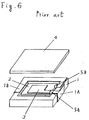
- Fig. 6 shows a perspective view of conventional crystal oscillator showing its construction
- Fig. 7 shows a cross-section thereof.
- Fig. 6 shows vibrating plate 2 of crystal oscillator sandwiched between the upper and lower electrodes 3, housed in a recess of lower casing 1.
- upper casing 4 is bonded on the upper surface of lower casing 1 sealing said vibrating plate 2 housed in said recess.
- vibrating plate 2 may be fixed irregularly within said recess causing an unstable oscillation of vibrating plate 2 if it is contacted with lower casing 1 or upper casing 4.
- the crystal oscillator of the present invention has an improved mechanical construction eliminating the possibilities of the contacts between the vibrating plate and the other components of crystal oscillator completely, and at the same time, has an improved construction supplying the current to the vibrating plate.
- the vibrating plate of the invented crystal oscillator comprised of a rim part, vibrating part surrounded by said rim part with a fine slit in-between, and a relatively narrow connecting part connecting said vibrating part to said rim part, and these three parts are made as one body by the same material.
- the relative position of said vibrating part to said rim part is permanently fixed, and no contact of the vibrating part and the rim part is possible.
- the vibrating part and the connecting part are made thinner than the thickness of the rim part, the vibrating part can never be contacted with the casings covering the both sides of the vibrating part.
- the vibrating part is provided with an electrode on both sides of the vibrating part, and an electrical lead which is an extension of said electrode on both sides of the connecting part also.
- the both sides of the vibrating part is covered by upper and lower casings, and each of the casings is provided with a through-hole at a position facing to said electrical lead.
- a cup-shaped metal lead is fixed on the internal surface of said through-hole, and the bottom of said cup-shaped metal lead is fixed on the electrical lead facing to the through-hole, and the metal lead is electrically connected to the electrical lead.
- the metal lead is fabricated by depositing metal particle on the through-hole employing either a vacuum evaporation or sputtering method. Therefore, the current can be supplied to the electrodes of vibrating part through said metal leads.
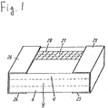
- Fig. 1 shows a perspective view of a first embodiment of the invented crystal oscillator
- Fig. 2 is an exploded view of the crystal oscillator shown in Fig. 1
- Fig. 3 is a partial exploded view of the crystal oscillator shown in Fig. 1.
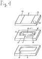
- Fig. 4 shows an exploded view of a second embodiment of the invention
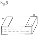
- Fig. 5 shows a perspective view of the second embodiment of the invention.
- Fig. 6 shows an exploded view of conventional crystal oscillator and Fig. 7 shows a cross-section of conventional crystal oscillator.
- Fig. 1 shows a perspective view of the invented crystal oscillator
- Fig. 2 shows an exploded view of the crystal oscillator shown in Fig. 1.
- rectangular lower casing is provided with recess 7.
- the vibrating plate 8 made of quartz crystal, consists of rim part 10, vibrating part 12 surrounded by rim part 10 with a slit part 13, and narrow connecting part 1 connecting vibrating part 12 to rim part 10, and holding vibrating part 12 in a cantilever fashion within the rim part 10. These three parts are made as one body by the same material.
- these three components including the upper casing 9, vibrating plate 8, and the lower casing 6 are stacked by using rim part 10.
- vibrating plate 8 and upper and lower casings 9 and 6 are made of quartz crystal, and the slit 13 separating rim part 10 from vibrating part 12 except at connecting part 11 is formed by employing an etching or sand-blasting method.
- connecting part 11 is made narrower than the width of vibrating part 12 so that very little of the vibration generated by vibrating part 12 is transmitted to connecting part 11.
- the thicknesses of these parts are made less than the thickness of rim part 10 including the thicknesses of the later described electrodes and electrical leads.
- the vibrating plate 8 is further provided with upper electrode 14 and lower electrode 15 (not shown in Fig. 2) on its respective surface, and the connecting part 11 is provided with upper electrical lead 16 and lower electrical lead 17 (not shown in Fig. 2) on its respective surface.
- Said upper electrical lead 16 and lower electrical lead 17 are extensions of the upper electrode 14 and the lower electrode 15 respectively, and these electrodes and electrical leads are fabricated usually by a gold deposition method.
- vibrating plate 8 comprised of rim part 10, vibrating part 12 surrounded by rim part 10 and slit part 13 formed within rim part 10, and relatively narrow connecting part 11 connecting vibrating part 12 to rim part 10, is made as one body by the same material. Therefore, the relative position of vibrating part 12 to rim part 10 is fixed, so that the possibility of contact of vibrating part 12 to rim part 10 can be avoided.
- vibrating part 12 and connecting part 11 including the thicknesses of the electrode and the electrical lead are made less than the thickness of rim part 10, vibrating part 12 can never be contacted with upper casing 9 or lower casing 6 even if it is in a vibrating mode. This means that vibrating part 12 can never be contacted with any other parts of crystal oscillator.
- recess 7 is provided in lower casing 6 in order to provide a still larger distance between the vibrating part 12 and the lower casing 6.
- a recess is provided in upper casing 9 also by the same reason, this is not shown in Fig. 2. If the depth of said recess is made adequately deep, the thickness of vibrating part 12 is not necessarily be made less than the thickness of rim part 10.
- Three components of upper casing 9, vibrating part 8, andower casing 6 are then stacked by taking the processes shown in the following.
- Fig. 3 shows a cross-section of lower metal lead 30. This can be fabricated by depositing metal particles evaporated from bottom to the upward direction on the inner wall of lower through-hole 18 using either a vacuum deposition or sputtering method.
- the lower metal lead 30 is deposited on the inner wall of lower through-hole 18 and lower electrical lead 17, effecting an electrical connection there-between. Gap 20 between the lower casing 6 and the lower electrical lead 17 is filled with the material deposited on lover electrical lead 17 of lower metal lead 30. As a result of this, lower through-hole 18 is sealed completely by lower metal lead 30.
- the length of gap 20 is about 2000 ⁇ and the thickness of the material filling gap 20 of lower metal lead 30 is about 6000 ⁇ . Since the inner wall of lower through-hole 18 is vertical, it is somewhat awkward to deposite metal particles vertically on the inner wall.
- therfore the number of metal particles which can be deposited on the inner wall of the through-hole is increased by employing a tapered through-hole construction as shown in Fig. 3.
- the thickness of the metal layer deposited on the tapered part of tapered hole is about 2000 ⁇ .
- Fig. 3 shows a cross-section of the joint established between the lower metal lead 30 and the right-side electrical terminal 25 (Fig.1) which consists of the printed silver-paste layer 22, nickel-plated layer 23, and solder-plated layer 24.
- the electrical connection to lower metal lead 30 is accomplished through the silver-paste layer 22.
- sealing glass 21 is added to metal lead 30.
- the sealing reliability could also be increased by adding silver-paste 22 into lower metal lead 30 in place of sealing glass 21.
- the addition of silver-paste 22 into lower metal lead 30 is effective to reduce the failure of electric disconnection of the metal lead due to the difficulty of deposition of metal particles on the inner wall of through-hole.
- Fig. 2 shows a connection between the upper metal lead 31 deposited on upper casing 9 and the left-side electrical termina 16.
- the connection of upper metal lead 31 to the left-side electrical terminal 26 is accomplished through conductive pattern 27.
- Glass layer 28 as an insulator layer is formed on conductive pattern 27, and the before-mentioned right-side electrical terminal 25 is formed on said glass layer 28.
- Figs. 4 and 5 show a second embodiment of the invention.
- the connecting part 11 is positioned at the center of longer edge of rectangular vibrating plate 8, and the vibrating part 12 is supported at the center of its longer edge in a cantilever fashion.
- the upper electrical lead 16 formed on the upper electrode 14 is extended toward right-side.
- lower electrode 15 and lower electrical lead 17 extended toward left-side are provided on the lower surface of vibrating part 12 also.
- the upper electrical lead 16 is connected to the right-side electrical terminal 25 by using through-hole 19 of upper casing 9, while the lower electrical lead 17 is connected to the left-side electrical terminal 26 through through-hole 18 of lower casing 6.
- the construction of the second embodiment is simpler because the conductive pattern 27 shown in Figs. 1 and 2 is not employed in there.
Landscapes
- Physics & Mathematics (AREA)
- Acoustics & Sound (AREA)
- Piezo-Electric Or Mechanical Vibrators, Or Delay Or Filter Circuits (AREA)
- Oscillators With Electromechanical Resonators (AREA)
Applications Claiming Priority (3)
| Application Number | Priority Date | Filing Date | Title |
|---|---|---|---|
| JP25045793 | 1993-10-06 | ||
| JP250457/93 | 1993-10-06 | ||
| JP5250457A JPH07106905A (ja) | 1993-10-06 | 1993-10-06 | 発振子 |
Publications (3)
| Publication Number | Publication Date |
|---|---|
| EP0648014A2 true EP0648014A2 (de) | 1995-04-12 |
| EP0648014A3 EP0648014A3 (de) | 1996-01-24 |
| EP0648014B1 EP0648014B1 (de) | 2001-07-18 |
Family
ID=17208166
Family Applications (1)
| Application Number | Title | Priority Date | Filing Date |
|---|---|---|---|
| EP94115829A Expired - Lifetime EP0648014B1 (de) | 1993-10-06 | 1994-10-06 | Kristallresonator |
Country Status (6)
| Country | Link |
|---|---|
| US (1) | US5596243A (de) |
| EP (1) | EP0648014B1 (de) |
| JP (1) | JPH07106905A (de) |
| KR (1) | KR0145370B1 (de) |
| CN (1) | CN1041681C (de) |
| DE (1) | DE69427730T2 (de) |
Cited By (1)
| Publication number | Priority date | Publication date | Assignee | Title |
|---|---|---|---|---|
| EP2081293A2 (de) | 2008-01-15 | 2009-07-22 | Nihon Dempa Kogyo Co., Ltd. | Kristallvorrichtungen und Verfahren zu deren Herstellung |
Families Citing this family (66)
| Publication number | Priority date | Publication date | Assignee | Title |
|---|---|---|---|---|
| US5458638A (en) * | 1989-07-06 | 1995-10-17 | Spine-Tech, Inc. | Non-threaded spinal implant |
| US6043588A (en) * | 1995-07-18 | 2000-03-28 | Murata Manufacturing Co., Ltd. | Piezoelectric sensor and acceleration sensor |
| JP3271517B2 (ja) * | 1996-04-05 | 2002-04-02 | 株式会社村田製作所 | 圧電共振子およびそれを用いた電子部品 |
| US6016024A (en) * | 1996-04-05 | 2000-01-18 | Murata Manufacturing Co., Ltd. | Piezoelectric component |
| JP3266031B2 (ja) * | 1996-04-18 | 2002-03-18 | 株式会社村田製作所 | 圧電共振子およびそれを用いた電子部品 |
| US5939819A (en) * | 1996-04-18 | 1999-08-17 | Murata Manufacturing Co., Ltd. | Electronic component and ladder filter |
| JPH1079639A (ja) * | 1996-07-10 | 1998-03-24 | Murata Mfg Co Ltd | 圧電共振子およびそれを用いた電子部品 |
| JPH1084244A (ja) * | 1996-07-18 | 1998-03-31 | Murata Mfg Co Ltd | 圧電共振子およびそれを用いた電子部品 |
| JP3271541B2 (ja) * | 1996-07-26 | 2002-04-02 | 株式会社村田製作所 | 圧電共振子およびそれを用いた電子部品 |
| JP3577170B2 (ja) * | 1996-08-05 | 2004-10-13 | 株式会社村田製作所 | 圧電共振子とその製造方法およびそれを用いた電子部品 |
| JPH10107579A (ja) * | 1996-08-06 | 1998-04-24 | Murata Mfg Co Ltd | 圧電部品 |
| JPH10126203A (ja) * | 1996-08-27 | 1998-05-15 | Murata Mfg Co Ltd | 圧電共振子およびそれを用いた電子部品 |
| JP3267171B2 (ja) * | 1996-09-12 | 2002-03-18 | 株式会社村田製作所 | 圧電共振子およびそれを用いた電子部品 |
| JPH10126202A (ja) * | 1996-10-23 | 1998-05-15 | Murata Mfg Co Ltd | 圧電共振子およびそれを用いた電子部品 |
| JP3271538B2 (ja) * | 1996-11-28 | 2002-04-02 | 株式会社村田製作所 | 圧電共振子およびそれを用いた電子部品 |
| JP2001060843A (ja) * | 1999-08-23 | 2001-03-06 | Murata Mfg Co Ltd | チップ型圧電部品 |
| US6590315B2 (en) * | 2000-05-26 | 2003-07-08 | William D. Beaver | Surface mount quartz crystal resonators and methods for making same |
| CN1162859C (zh) * | 2000-06-08 | 2004-08-18 | 新科实业有限公司 | 采用环形旋转压电执行机构的高密度硬盘驱动器的双级执行机构系统 |
| CN100344740C (zh) * | 2002-08-05 | 2007-10-24 | 新日本石油株式会社 | 润滑油组合物 |
| CN101142742B (zh) * | 2005-04-18 | 2011-06-15 | 株式会社大真空 | 压电振动片和压电振动器件 |
| JP4729766B2 (ja) | 2006-08-10 | 2011-07-20 | 独立行政法人産業技術総合研究所 | 超電導酸化物材料の製造方法 |
| US7564177B2 (en) * | 2006-12-26 | 2009-07-21 | Nihon Dempa Kogyo Co., Ltd. | Crystal unit having stacked structure |
| JP5327932B2 (ja) | 2007-02-08 | 2013-10-30 | 独立行政法人産業技術総合研究所 | 超電導コーティング材料の製造方法 |
| JP5078512B2 (ja) * | 2007-09-06 | 2012-11-21 | 日本電波工業株式会社 | 水晶デバイス |
| JP5329105B2 (ja) * | 2008-02-25 | 2013-10-30 | 京セラクリスタルデバイス株式会社 | 水晶振動子の製造方法 |
| US8476809B2 (en) | 2008-04-29 | 2013-07-02 | Sand 9, Inc. | Microelectromechanical systems (MEMS) resonators and related apparatus and methods |
| US8410868B2 (en) | 2009-06-04 | 2013-04-02 | Sand 9, Inc. | Methods and apparatus for temperature control of devices and mechanical resonating structures |
| JP4647677B2 (ja) | 2008-08-11 | 2011-03-09 | 日本電波工業株式会社 | 圧電デバイス |
| USD630597S1 (en) * | 2009-02-04 | 2011-01-11 | Nihon Dempa Kogyo Co., Ltd. | Crystal unit |
| JP4851549B2 (ja) * | 2009-02-10 | 2012-01-11 | 日本電波工業株式会社 | 圧電デバイス |
| US9048811B2 (en) | 2009-03-31 | 2015-06-02 | Sand 9, Inc. | Integration of piezoelectric materials with substrates |
| WO2010114602A1 (en) * | 2009-03-31 | 2010-10-07 | Sand9, Inc. | Integration of piezoelectric materials with substrates |
| USD646236S1 (en) * | 2009-11-05 | 2011-10-04 | Seiko Instruments Inc. | Quartz crystal |
| USD643385S1 (en) * | 2009-11-06 | 2011-08-16 | Seiko Instruments Inc. | Quartz crystal |
| USD634287S1 (en) * | 2009-11-06 | 2011-03-15 | Seiko Instruments Inc. | Quartz crystal |
| USD643383S1 (en) * | 2009-11-06 | 2011-08-16 | Seiko Instruments Inc. | Quartz crystal |
| USD653631S1 (en) * | 2009-11-06 | 2012-02-07 | Seiko Instruments Inc. | Quartz crystal |
| USD643382S1 (en) * | 2009-11-06 | 2011-08-16 | Seiko Instruments Inc. | Quartz crystal |
| JP5445982B2 (ja) | 2009-12-09 | 2014-03-19 | 独立行政法人産業技術総合研究所 | 希土類超電導膜形成用溶液およびその製造方法 |
| JP5476964B2 (ja) | 2009-12-09 | 2014-04-23 | セイコーエプソン株式会社 | 振動子、発振器、ジャイロ及び電子機器 |
| USD643384S1 (en) * | 2010-03-29 | 2011-08-16 | Seiko Instruments Inc. | Quartz crystal |
| USD643387S1 (en) * | 2010-03-29 | 2011-08-16 | Seiko Instruments Inc. | Quartz crystal |
| USD634288S1 (en) * | 2010-03-29 | 2011-03-15 | Seiko Instruments Inc. | Quartz crystal |
| USD646237S1 (en) * | 2010-03-29 | 2011-10-04 | Seiko Instruments Inc. | Quartz crystal |
| USD643386S1 (en) * | 2010-03-29 | 2011-08-16 | Seiko Instruments Inc. | Quartz crystal |
| USD653632S1 (en) * | 2010-03-29 | 2012-02-07 | Seiko Instruments Inc. | Quartz crystal |
| USD646655S1 (en) * | 2010-06-16 | 2011-10-11 | Seiko Instruments Inc. | Quartz crystal |
| USD646649S1 (en) * | 2010-06-16 | 2011-10-11 | Seiko Instruments Inc. | Quartz crystal |
| USD648288S1 (en) * | 2010-06-16 | 2011-11-08 | Seiko Instruments Inc. | Quartz crystal |
| USD646651S1 (en) * | 2010-06-16 | 2011-10-11 | Seiko Instruments Inc. | Quartz crystal |
| USD646656S1 (en) * | 2010-06-16 | 2011-10-11 | Seiko Instruments Inc. | Quartz crystal |
| USD647071S1 (en) * | 2010-06-16 | 2011-10-18 | Seiko Instruments Inc. | Quartz crystal |
| USD646650S1 (en) * | 2010-06-16 | 2011-10-11 | Seiko Instruments Inc. | Quartz crystal |
| USD646653S1 (en) * | 2010-06-16 | 2011-10-11 | Seiko Instruments Inc. | Quartz crystal |
| USD646654S1 (en) * | 2010-06-16 | 2011-10-11 | Seiko Instruments Inc. | Quartz crystal |
| USD646648S1 (en) * | 2010-06-16 | 2011-10-11 | Seiko Instruments Inc. | Quartz crystal |
| USD637982S1 (en) * | 2010-06-16 | 2011-05-17 | Seiko Instruments Inc. | Quartz crystal |
| USD646652S1 (en) * | 2010-06-16 | 2011-10-11 | Seiko Instruments Inc. | Quartz crystal |
| JP5447316B2 (ja) * | 2010-09-21 | 2014-03-19 | 株式会社大真空 | 電子部品パッケージ用封止部材、及び電子部品パッケージ |
| CN102394589B (zh) * | 2011-10-09 | 2014-02-12 | 浙江雅晶电子有限公司 | 一种用于定位晶振和支架的定位装置 |
| WO2014123519A1 (en) | 2013-02-06 | 2014-08-14 | Empire Technology Development Llc | Devices, systems, and methods for detecting odorants |
| US9879997B1 (en) * | 2013-11-19 | 2018-01-30 | Hrl Laboratories, Llc | Quartz resonator with plasma etched tethers for stress isolation from the mounting contacts |
| US20170040971A1 (en) * | 2014-01-30 | 2017-02-09 | Empire Technology Development Llc | Crystal oscillators and methods for fabricating the same |
| US9977097B1 (en) | 2014-02-21 | 2018-05-22 | Hrl Laboratories, Llc | Micro-scale piezoelectric resonating magnetometer |
| US10031191B1 (en) | 2015-01-16 | 2018-07-24 | Hrl Laboratories, Llc | Piezoelectric magnetometer capable of sensing a magnetic field in multiple vectors |
| CN111508926B (zh) * | 2019-01-31 | 2022-08-30 | 奥特斯(中国)有限公司 | 一种部件承载件以及制造部件承载件的方法 |
Family Cites Families (16)
| Publication number | Priority date | Publication date | Assignee | Title |
|---|---|---|---|---|
| JPS5398793A (en) * | 1977-02-09 | 1978-08-29 | Seiko Epson Corp | Piezo electric vibrator |
| JPS5513553A (en) * | 1978-07-14 | 1980-01-30 | Matsushima Kogyo Co Ltd | Crystal vibrator |
| JPS5538748A (en) * | 1978-09-11 | 1980-03-18 | Matsushima Kogyo Co Ltd | Resonator |
| FR2441960A1 (fr) * | 1978-11-16 | 1980-06-13 | Suisse Horlogerie | Resonateur piezoelectrique travaillant en cisaillement d'epaisseur |
| CH626479A5 (de) * | 1979-07-05 | 1981-11-13 | Suisse Horlogerie | |
| CH625372A5 (de) * | 1979-07-06 | 1981-09-15 | Ebauchesfabrik Eta Ag | |
| US4421621A (en) * | 1979-07-17 | 1983-12-20 | Kabushiki Kaisha Suwa Seikosha | Quartz crystal oscillator |
| US4540909A (en) * | 1983-04-04 | 1985-09-10 | Seiko Instruments & Electronics Ltd. | Tuning fork type quartz crystal resonator with variable width base |
| FR2547458B3 (fr) * | 1983-06-07 | 1986-02-21 | Electronique Piezoelectricite | Resonateur piezoelectrique pourvu d'un dispositif d'encapsulation |
| JPS61202508A (ja) * | 1985-03-06 | 1986-09-08 | Matsushima Kogyo Co Ltd | 圧電振動子 |
| JPS6227040A (ja) * | 1985-07-26 | 1987-02-05 | Sapporo Breweries Ltd | 物質を澱粉に吸着あるいは包接させる方法 |
| US4763078A (en) * | 1986-03-27 | 1988-08-09 | Williams Bruce T | Sensor for electrostatic voltmeter |
| JPH07112004B2 (ja) * | 1986-11-11 | 1995-11-29 | 富士通株式会社 | 半導体装置の製造方法 |
| GB2202989B (en) * | 1987-04-02 | 1991-01-09 | Stc Plc | Crystal resonnator |
| US5101669A (en) * | 1988-07-14 | 1992-04-07 | University Of Hawaii | Multidimensional force sensor |
| KR0158469B1 (ko) * | 1992-10-15 | 1999-03-20 | 모리시타 요이찌 | 발진자 |
-
1993
- 1993-10-06 JP JP5250457A patent/JPH07106905A/ja active Pending
-
1994
- 1994-08-23 CN CN94115802A patent/CN1041681C/zh not_active Expired - Fee Related
- 1994-10-04 KR KR1019940025276A patent/KR0145370B1/ko not_active Expired - Fee Related
- 1994-10-05 US US08/318,336 patent/US5596243A/en not_active Expired - Lifetime
- 1994-10-06 DE DE69427730T patent/DE69427730T2/de not_active Expired - Fee Related
- 1994-10-06 EP EP94115829A patent/EP0648014B1/de not_active Expired - Lifetime
Cited By (3)
| Publication number | Priority date | Publication date | Assignee | Title |
|---|---|---|---|---|
| EP2081293A2 (de) | 2008-01-15 | 2009-07-22 | Nihon Dempa Kogyo Co., Ltd. | Kristallvorrichtungen und Verfahren zu deren Herstellung |
| EP2081293A3 (de) * | 2008-01-15 | 2009-11-18 | Nihon Dempa Kogyo Co., Ltd. | Kristallvorrichtungen und Verfahren zu deren Herstellung |
| US7932662B2 (en) | 2008-01-15 | 2011-04-26 | Nihon Dempa Kogyo Co., Ltd. | Crystal devices and methods for manufacturing same |
Also Published As
| Publication number | Publication date |
|---|---|
| CN1041681C (zh) | 1999-01-13 |
| JPH07106905A (ja) | 1995-04-21 |
| US5596243A (en) | 1997-01-21 |
| DE69427730T2 (de) | 2001-10-31 |
| EP0648014B1 (de) | 2001-07-18 |
| KR0145370B1 (ko) | 1998-08-17 |
| CN1105165A (zh) | 1995-07-12 |
| EP0648014A3 (de) | 1996-01-24 |
| KR950013023A (ko) | 1995-05-17 |
| DE69427730D1 (de) | 2001-08-23 |
Similar Documents
| Publication | Publication Date | Title |
|---|---|---|
| EP0648014B1 (de) | Kristallresonator | |
| US5545849A (en) | Electronic component device and its manufacturing method | |
| JPH0435108A (ja) | 超薄板多重モード水晶フィルタ素子 | |
| JP2002009576A (ja) | 圧電デバイス及びそのパッケージ構造 | |
| US4112324A (en) | Mounting for plural piezoelectric vibrator units | |
| CN112703672B (zh) | 谐振子以及谐振装置 | |
| JP3498568B2 (ja) | 圧電振動子ユニットおよび圧電発振器 | |
| JP2018056860A (ja) | 水晶素子、水晶デバイスおよび水晶素子の製造方法 | |
| JP2007274339A (ja) | 表面実装型圧電振動デバイス | |
| JPH1051265A (ja) | 表面実装型水晶振動子 | |
| JPS59119911A (ja) | 圧電振動子 | |
| JPH0774581A (ja) | 圧電振動子 | |
| WO2023112380A1 (ja) | 共振子及び共振装置 | |
| CN113302838B (zh) | 振动元件、振子以及振动元件的制造方法 | |
| JP5599057B2 (ja) | パッケージおよび圧電振動子 | |
| JP2006074567A (ja) | 圧電デバイス | |
| JP2018056861A (ja) | 水晶素子および水晶デバイス | |
| JP2008167402A (ja) | 圧電振動片、圧電デバイスおよび圧電振動片の製造方法 | |
| US6376970B1 (en) | Piezoelectric resonator supporting structure and a piezoelectric component including the same | |
| US20250047257A1 (en) | Base for piezoelectric device, manufacturing method therefor, and piezoelectric device | |
| JPH08204496A (ja) | 圧電振動部品 | |
| JP2008301297A (ja) | 水晶デバイス | |
| JPS5848818Y2 (ja) | 圧電振動子の保持容器 | |
| JP4833716B2 (ja) | 圧電発振器 | |
| JPH08316762A (ja) | 振動子の製造方法 |
Legal Events
| Date | Code | Title | Description |
|---|---|---|---|
| PUAI | Public reference made under article 153(3) epc to a published international application that has entered the european phase |
Free format text: ORIGINAL CODE: 0009012 |
|
| AK | Designated contracting states |
Kind code of ref document: A2 Designated state(s): DE FR GB |
|
| PUAL | Search report despatched |
Free format text: ORIGINAL CODE: 0009013 |
|
| AK | Designated contracting states |
Kind code of ref document: A3 Designated state(s): DE FR GB |
|
| 17P | Request for examination filed |
Effective date: 19960412 |
|
| 17Q | First examination report despatched |
Effective date: 19990408 |
|
| GRAG | Despatch of communication of intention to grant |
Free format text: ORIGINAL CODE: EPIDOS AGRA |
|
| GRAG | Despatch of communication of intention to grant |
Free format text: ORIGINAL CODE: EPIDOS AGRA |
|
| GRAH | Despatch of communication of intention to grant a patent |
Free format text: ORIGINAL CODE: EPIDOS IGRA |
|
| GRAH | Despatch of communication of intention to grant a patent |
Free format text: ORIGINAL CODE: EPIDOS IGRA |
|
| GRAA | (expected) grant |
Free format text: ORIGINAL CODE: 0009210 |
|
| AK | Designated contracting states |
Kind code of ref document: B1 Designated state(s): DE FR GB |
|
| REF | Corresponds to: |
Ref document number: 69427730 Country of ref document: DE Date of ref document: 20010823 |
|
| PGFP | Annual fee paid to national office [announced via postgrant information from national office to epo] |
Ref country code: GB Payment date: 20010925 Year of fee payment: 8 |
|
| PGFP | Annual fee paid to national office [announced via postgrant information from national office to epo] |
Ref country code: FR Payment date: 20011018 Year of fee payment: 8 |
|
| PGFP | Annual fee paid to national office [announced via postgrant information from national office to epo] |
Ref country code: DE Payment date: 20011129 Year of fee payment: 8 |
|
| ET | Fr: translation filed | ||
| REG | Reference to a national code |
Ref country code: GB Ref legal event code: IF02 |
|
| PLBE | No opposition filed within time limit |
Free format text: ORIGINAL CODE: 0009261 |
|
| STAA | Information on the status of an ep patent application or granted ep patent |
Free format text: STATUS: NO OPPOSITION FILED WITHIN TIME LIMIT |
|
| 26N | No opposition filed | ||
| PG25 | Lapsed in a contracting state [announced via postgrant information from national office to epo] |
Ref country code: GB Free format text: LAPSE BECAUSE OF NON-PAYMENT OF DUE FEES Effective date: 20021006 |
|
| PG25 | Lapsed in a contracting state [announced via postgrant information from national office to epo] |
Ref country code: DE Free format text: LAPSE BECAUSE OF NON-PAYMENT OF DUE FEES Effective date: 20030501 |
|
| GBPC | Gb: european patent ceased through non-payment of renewal fee |
Effective date: 20021006 |
|
| PG25 | Lapsed in a contracting state [announced via postgrant information from national office to epo] |
Ref country code: FR Free format text: LAPSE BECAUSE OF NON-PAYMENT OF DUE FEES Effective date: 20030630 |
|
| REG | Reference to a national code |
Ref country code: FR Ref legal event code: ST |