EP0649748A2 - Tête thermique pour imprimantes - Google Patents
Tête thermique pour imprimantes Download PDFInfo
- Publication number
- EP0649748A2 EP0649748A2 EP94116818A EP94116818A EP0649748A2 EP 0649748 A2 EP0649748 A2 EP 0649748A2 EP 94116818 A EP94116818 A EP 94116818A EP 94116818 A EP94116818 A EP 94116818A EP 0649748 A2 EP0649748 A2 EP 0649748A2
- Authority
- EP
- European Patent Office
- Prior art keywords
- film
- thermal head
- resistor
- heat generating
- resistor film
- Prior art date
- Legal status (The legal status is an assumption and is not a legal conclusion. Google has not performed a legal analysis and makes no representation as to the accuracy of the status listed.)
- Granted
Links
- 239000004020 conductor Substances 0.000 claims abstract description 32
- 239000011241 protective layer Substances 0.000 claims abstract description 29
- 239000000758 substrate Substances 0.000 claims abstract description 26
- 229910052715 tantalum Inorganic materials 0.000 claims abstract description 18
- GUVRBAGPIYLISA-UHFFFAOYSA-N tantalum atom Chemical compound [Ta] GUVRBAGPIYLISA-UHFFFAOYSA-N 0.000 claims abstract description 16
- 230000003647 oxidation Effects 0.000 claims abstract description 15
- 238000007254 oxidation reaction Methods 0.000 claims abstract description 15
- 238000000059 patterning Methods 0.000 claims abstract description 15
- 239000002344 surface layer Substances 0.000 claims abstract description 8
- 239000010410 layer Substances 0.000 claims description 44
- 238000004544 sputter deposition Methods 0.000 claims description 24
- 239000000463 material Substances 0.000 claims description 18
- 238000000034 method Methods 0.000 claims description 14
- 238000000151 deposition Methods 0.000 claims description 11
- 238000000206 photolithography Methods 0.000 claims description 10
- XUIMIQQOPSSXEZ-UHFFFAOYSA-N Silicon Chemical compound [Si] XUIMIQQOPSSXEZ-UHFFFAOYSA-N 0.000 claims description 8
- 239000011261 inert gas Substances 0.000 claims description 8
- 229910052710 silicon Inorganic materials 0.000 claims description 8
- 239000010703 silicon Substances 0.000 claims description 8
- XKRFYHLGVUSROY-UHFFFAOYSA-N Argon Chemical compound [Ar] XKRFYHLGVUSROY-UHFFFAOYSA-N 0.000 claims description 6
- 229910052581 Si3N4 Inorganic materials 0.000 claims description 6
- HQVNEWCFYHHQES-UHFFFAOYSA-N silicon nitride Chemical group N12[Si]34N5[Si]62N3[Si]51N64 HQVNEWCFYHHQES-UHFFFAOYSA-N 0.000 claims description 6
- 239000010936 titanium Substances 0.000 claims description 6
- 229910052719 titanium Inorganic materials 0.000 claims description 6
- 239000007789 gas Substances 0.000 claims description 5
- RTAQQCXQSZGOHL-UHFFFAOYSA-N Titanium Chemical compound [Ti] RTAQQCXQSZGOHL-UHFFFAOYSA-N 0.000 claims description 4
- VYPSYNLAJGMNEJ-UHFFFAOYSA-N Silicium dioxide Chemical compound O=[Si]=O VYPSYNLAJGMNEJ-UHFFFAOYSA-N 0.000 claims description 3
- 229910052786 argon Inorganic materials 0.000 claims description 3
- 230000001590 oxidative effect Effects 0.000 claims description 3
- 229910052814 silicon oxide Inorganic materials 0.000 claims description 3
- 229910052758 niobium Inorganic materials 0.000 claims description 2
- 239000010955 niobium Substances 0.000 claims description 2
- GUCVJGMIXFAOAE-UHFFFAOYSA-N niobium atom Chemical compound [Nb] GUCVJGMIXFAOAE-UHFFFAOYSA-N 0.000 claims description 2
- 239000002253 acid Substances 0.000 claims 3
- 229910001257 Nb alloy Inorganic materials 0.000 claims 1
- 229910001362 Ta alloys Inorganic materials 0.000 claims 1
- 229910001069 Ti alloy Inorganic materials 0.000 claims 1
- 150000002822 niobium compounds Chemical class 0.000 claims 1
- 150000003482 tantalum compounds Chemical class 0.000 claims 1
- 150000003609 titanium compounds Chemical class 0.000 claims 1
- 230000004043 responsiveness Effects 0.000 abstract description 4
- 239000010408 film Substances 0.000 description 94
- 238000010438 heat treatment Methods 0.000 description 33
- 230000020169 heat generation Effects 0.000 description 18
- 238000009826 distribution Methods 0.000 description 14
- 238000004088 simulation Methods 0.000 description 12
- 238000004519 manufacturing process Methods 0.000 description 8
- XAGFODPZIPBFFR-UHFFFAOYSA-N aluminium Chemical compound [Al] XAGFODPZIPBFFR-UHFFFAOYSA-N 0.000 description 7
- 229910052782 aluminium Inorganic materials 0.000 description 7
- NBIIXXVUZAFLBC-UHFFFAOYSA-N Phosphoric acid Chemical compound OP(O)(O)=O NBIIXXVUZAFLBC-UHFFFAOYSA-N 0.000 description 4
- 238000005530 etching Methods 0.000 description 4
- PBCFLUZVCVVTBY-UHFFFAOYSA-N tantalum pentoxide Chemical compound O=[Ta](=O)O[Ta](=O)=O PBCFLUZVCVVTBY-UHFFFAOYSA-N 0.000 description 4
- QTBSBXVTEAMEQO-UHFFFAOYSA-N Acetic acid Chemical compound CC(O)=O QTBSBXVTEAMEQO-UHFFFAOYSA-N 0.000 description 3
- 239000007788 liquid Substances 0.000 description 3
- 238000012360 testing method Methods 0.000 description 3
- RYGMFSIKBFXOCR-UHFFFAOYSA-N Copper Chemical compound [Cu] RYGMFSIKBFXOCR-UHFFFAOYSA-N 0.000 description 2
- 229910045601 alloy Inorganic materials 0.000 description 2
- 239000000956 alloy Substances 0.000 description 2
- 229910000147 aluminium phosphate Inorganic materials 0.000 description 2
- QVGXLLKOCUKJST-UHFFFAOYSA-N atomic oxygen Chemical compound [O] QVGXLLKOCUKJST-UHFFFAOYSA-N 0.000 description 2
- 238000005229 chemical vapour deposition Methods 0.000 description 2
- 150000001875 compounds Chemical class 0.000 description 2
- 238000010276 construction Methods 0.000 description 2
- 239000010949 copper Substances 0.000 description 2
- 229910052802 copper Inorganic materials 0.000 description 2
- 238000009792 diffusion process Methods 0.000 description 2
- 239000007772 electrode material Substances 0.000 description 2
- 238000002474 experimental method Methods 0.000 description 2
- 238000012986 modification Methods 0.000 description 2
- 230000004048 modification Effects 0.000 description 2
- TWNQGVIAIRXVLR-UHFFFAOYSA-N oxo(oxoalumanyloxy)alumane Chemical compound O=[Al]O[Al]=O TWNQGVIAIRXVLR-UHFFFAOYSA-N 0.000 description 2
- 239000001301 oxygen Substances 0.000 description 2
- 229910052760 oxygen Inorganic materials 0.000 description 2
- BPUBBGLMJRNUCC-UHFFFAOYSA-N oxygen(2-);tantalum(5+) Chemical compound [O-2].[O-2].[O-2].[O-2].[O-2].[Ta+5].[Ta+5] BPUBBGLMJRNUCC-UHFFFAOYSA-N 0.000 description 2
- 238000012546 transfer Methods 0.000 description 2
- DDFHBQSCUXNBSA-UHFFFAOYSA-N 5-(5-carboxythiophen-2-yl)thiophene-2-carboxylic acid Chemical compound S1C(C(=O)O)=CC=C1C1=CC=C(C(O)=O)S1 DDFHBQSCUXNBSA-UHFFFAOYSA-N 0.000 description 1
- 229910000838 Al alloy Inorganic materials 0.000 description 1
- 229910000881 Cu alloy Inorganic materials 0.000 description 1
- GRYLNZFGIOXLOG-UHFFFAOYSA-N Nitric acid Chemical compound O[N+]([O-])=O GRYLNZFGIOXLOG-UHFFFAOYSA-N 0.000 description 1
- 229910000676 Si alloy Inorganic materials 0.000 description 1
- 230000002378 acidificating effect Effects 0.000 description 1
- RVSGESPTHDDNTH-UHFFFAOYSA-N alumane;tantalum Chemical compound [AlH3].[Ta] RVSGESPTHDDNTH-UHFFFAOYSA-N 0.000 description 1
- CSDREXVUYHZDNP-UHFFFAOYSA-N alumanylidynesilicon Chemical compound [Al].[Si] CSDREXVUYHZDNP-UHFFFAOYSA-N 0.000 description 1
- WPPDFTBPZNZZRP-UHFFFAOYSA-N aluminum copper Chemical compound [Al].[Cu] WPPDFTBPZNZZRP-UHFFFAOYSA-N 0.000 description 1
- 239000007864 aqueous solution Substances 0.000 description 1
- 230000003190 augmentative effect Effects 0.000 description 1
- 230000008021 deposition Effects 0.000 description 1
- 238000007599 discharging Methods 0.000 description 1
- 230000000694 effects Effects 0.000 description 1
- 238000010292 electrical insulation Methods 0.000 description 1
- 230000002708 enhancing effect Effects 0.000 description 1
- 230000002349 favourable effect Effects 0.000 description 1
- 230000008642 heat stress Effects 0.000 description 1
- 238000009413 insulation Methods 0.000 description 1
- 239000011259 mixed solution Substances 0.000 description 1
- 229910017604 nitric acid Inorganic materials 0.000 description 1
- 150000004767 nitrides Chemical class 0.000 description 1
- 229920002120 photoresistant polymer Polymers 0.000 description 1
- 238000007788 roughening Methods 0.000 description 1
- 230000035939 shock Effects 0.000 description 1
- MZLGASXMSKOWSE-UHFFFAOYSA-N tantalum nitride Chemical compound [Ta]#N MZLGASXMSKOWSE-UHFFFAOYSA-N 0.000 description 1
- 229910001936 tantalum oxide Inorganic materials 0.000 description 1
- 239000010409 thin film Substances 0.000 description 1
Images



Classifications
-
- B—PERFORMING OPERATIONS; TRANSPORTING
- B41—PRINTING; LINING MACHINES; TYPEWRITERS; STAMPS
- B41J—TYPEWRITERS; SELECTIVE PRINTING MECHANISMS, i.e. MECHANISMS PRINTING OTHERWISE THAN FROM A FORME; CORRECTION OF TYPOGRAPHICAL ERRORS
- B41J2/00—Typewriters or selective printing mechanisms characterised by the printing or marking process for which they are designed
- B41J2/315—Typewriters or selective printing mechanisms characterised by the printing or marking process for which they are designed characterised by selective application of heat to a heat sensitive printing or impression-transfer material
- B41J2/32—Typewriters or selective printing mechanisms characterised by the printing or marking process for which they are designed characterised by selective application of heat to a heat sensitive printing or impression-transfer material using thermal heads
- B41J2/335—Structure of thermal heads
- B41J2/33505—Constructional details
- B41J2/33515—Heater layers
-
- B—PERFORMING OPERATIONS; TRANSPORTING
- B41—PRINTING; LINING MACHINES; TYPEWRITERS; STAMPS
- B41J—TYPEWRITERS; SELECTIVE PRINTING MECHANISMS, i.e. MECHANISMS PRINTING OTHERWISE THAN FROM A FORME; CORRECTION OF TYPOGRAPHICAL ERRORS
- B41J2/00—Typewriters or selective printing mechanisms characterised by the printing or marking process for which they are designed
- B41J2/315—Typewriters or selective printing mechanisms characterised by the printing or marking process for which they are designed characterised by selective application of heat to a heat sensitive printing or impression-transfer material
- B41J2/32—Typewriters or selective printing mechanisms characterised by the printing or marking process for which they are designed characterised by selective application of heat to a heat sensitive printing or impression-transfer material using thermal heads
- B41J2/335—Structure of thermal heads
- B41J2/33505—Constructional details
- B41J2/3353—Protective layers
-
- B—PERFORMING OPERATIONS; TRANSPORTING
- B41—PRINTING; LINING MACHINES; TYPEWRITERS; STAMPS
- B41J—TYPEWRITERS; SELECTIVE PRINTING MECHANISMS, i.e. MECHANISMS PRINTING OTHERWISE THAN FROM A FORME; CORRECTION OF TYPOGRAPHICAL ERRORS
- B41J2/00—Typewriters or selective printing mechanisms characterised by the printing or marking process for which they are designed
- B41J2/315—Typewriters or selective printing mechanisms characterised by the printing or marking process for which they are designed characterised by selective application of heat to a heat sensitive printing or impression-transfer material
- B41J2/32—Typewriters or selective printing mechanisms characterised by the printing or marking process for which they are designed characterised by selective application of heat to a heat sensitive printing or impression-transfer material using thermal heads
- B41J2/335—Structure of thermal heads
- B41J2/33545—Structure of thermal heads characterised by dimensions
-
- B—PERFORMING OPERATIONS; TRANSPORTING
- B41—PRINTING; LINING MACHINES; TYPEWRITERS; STAMPS
- B41J—TYPEWRITERS; SELECTIVE PRINTING MECHANISMS, i.e. MECHANISMS PRINTING OTHERWISE THAN FROM A FORME; CORRECTION OF TYPOGRAPHICAL ERRORS
- B41J2/00—Typewriters or selective printing mechanisms characterised by the printing or marking process for which they are designed
- B41J2/315—Typewriters or selective printing mechanisms characterised by the printing or marking process for which they are designed characterised by selective application of heat to a heat sensitive printing or impression-transfer material
- B41J2/32—Typewriters or selective printing mechanisms characterised by the printing or marking process for which they are designed characterised by selective application of heat to a heat sensitive printing or impression-transfer material using thermal heads
- B41J2/335—Structure of thermal heads
- B41J2/3355—Structure of thermal heads characterised by materials
-
- B—PERFORMING OPERATIONS; TRANSPORTING
- B41—PRINTING; LINING MACHINES; TYPEWRITERS; STAMPS
- B41J—TYPEWRITERS; SELECTIVE PRINTING MECHANISMS, i.e. MECHANISMS PRINTING OTHERWISE THAN FROM A FORME; CORRECTION OF TYPOGRAPHICAL ERRORS
- B41J2/00—Typewriters or selective printing mechanisms characterised by the printing or marking process for which they are designed
- B41J2/315—Typewriters or selective printing mechanisms characterised by the printing or marking process for which they are designed characterised by selective application of heat to a heat sensitive printing or impression-transfer material
- B41J2/32—Typewriters or selective printing mechanisms characterised by the printing or marking process for which they are designed characterised by selective application of heat to a heat sensitive printing or impression-transfer material using thermal heads
- B41J2/335—Structure of thermal heads
- B41J2/33555—Structure of thermal heads characterised by type
- B41J2/3357—Surface type resistors
Definitions
- This invention relates to a thermal head for ink-jet printers or thermal printers including thermal transfer printers.
- Thermal printers and ink-jet printers are largely used as output devices for computers and wordprocessors.
- thermal printers use a thermal head having an array of heat generating zones formed on an insulated substrate by thin-film techniques.
- the heat generating zones can be energized selectively individually to print dots in selected patterns.
- Each heat generating zone is defined between two opposite electrodes formed by patterning a conductor film, and a resistor film exists in each heat generating zone.
- the electrodes and the resistor film are covered with a protective layer. Heat generated in each heating zone is transferred to a thermographic paper or a heat-sensitive ribbon which makes contact with protective layer above the heat generating zone.
- Many of conventional ink-jet Printers also use a thermal head of fundamentally the same construction.
- the thermal head In ink-jet printers the thermal head is placed in the ink, and each heat generating zone of the thermal head heats a fraction of the ink to boil and produce a bubble which causes a droplet of the ink to spout from a nozzle or orifice above the heat generating zone.
- JP 61-260604 A shows a thermal head for thermal printers.
- the thermal head is produced by the steps of depositing a resistor film such as a tantalum film on an insulated substrate, depositing a conductor film such as an aluminum or copper film on the resistor film, patterning the conductor film so as to form two opposite electrodes for each heat generating zone and expose the resistor film in each heat generating zone, anodically oxidising the surface of the resistor film in each heat generating zone and finally forming a protective layer such as an oxide or nitride layer on both the electrodes and the anodically oxidized resistor surface.
- the conductor film, resistor film and the protective layer are formed by sputtering methods. That is, the fabrication of the thermal head entails three different sputtering operations. Since sputtering operations are costly due to the expensiveness of sputtering apparatus and targets, the thermal head is relatively high in production cost.
- the thermal head construction shown in JP 61-260604 A in ink-jet printers.
- the protective layer formed by sputtering is microscopically porous, it is necessary to increase the thickness of the protective layer.
- the thickened protective layer becomes large in heat capacity, and for this reason it is difficult to enhance the responsiveness and printing speed of the thermal head, and the power consumption of the thermal head increases.
- the responsiveness was about 10 kHz and the minimum input power for each heat generating zone to produce a bubble in the ink was 1000 W/mm2.
- JP 60-109850 A shows a thermal head for ink-jet printers.
- the thermal head is produced by the steps of depositing a resistor film (tantalum film) on an insulated substrate by sputtering, depositing a conductor film (aluminum film) on the resistor film, patterning the conductor film so as to form two opposite electrodes for each heat generating zone and exposing the resistor film in the heat generating zones and anodically oxidizing the surfaces of the electrodes and the exposed resistor film to form a protective layer of aluminum oxide on the electrodes and a protective layer of tantalum pentoxide Ta2O5 on the resistor surface.
- this thermal head entails only two sputtering operations for forming the resistor and conductor films, respectively. This is favorable for a cost reduction.
- problems about the anodixally oxidized protective layers The aluminum oxide layer on the electrodes and the tantalum oxide layer on the resistor film are chemically dissimilar and hence do not chemically bond to each other. Therefore, microscopic slits are liable to appear at the borders between these two layers as a cause of intrusion of the ink.
- durability of the thermal head may not be sufficient because during operation of the thermal head heat stresses will appear in the border regions of the two different protective layers. Another reason for the insufficient durability is the difficulty of employing optimal conditions for anodic oxidation of the electrodes and the resistor.
- Optimal conditions for anodic oxidation of the electrodes differ from optimal conditions for anodic oxidation of the resistor (tantalum), but the electrodes and the resistor have to be anodically oxidized simultaneously. Therefore, the actually employed conditions are not optimal for one or both of the electrodes and the resistor.
- the durability of this thermal head was at the order of 106 pulses, and failures of the samples were always attributed to a break at the border between the two different protective layers.
- a thermal head comprises a substrate having an insulating surface on which a plurality of heat generating zones are located in a predetermined arrangement, a patterned conductor film which lies on the insulating surface of the substrate and, for each of the heat generating zones, forms two opposite electrodes one of which terminates at an edge of the heat generating zone and the other at the opposite edge, a patterned resistor film which is formed of an anodically oxidizable material and continuously covers the patterned conductor film and the insulating surface in the heat generating zones, and a protective layer which is formed by anodic oxidation of a surface layer of the patterned resistor film.
- the principal feature of the invention is that the anodically oxidizable resistor film is deposited after the deposition and patterning of the conductor film. Since the patterned conductor film is entirely covered with the resistor film, the anodic oxidation of the surface of the resistor film can be performed under optimum conditions for the employed resistor material. Therefore, a protective layer of very good quality can be formed to thereby enhance durability of the thermal head. Furthermore, it is possible to greatly reduce the thicknesses of the protective layer and the resistor film to thereby reduce power consumption of the thermal head and enhance responsiveness.
- a preferred example of anodically oxidizable resistor materials is tantalum.
- the invention is useful for both ink-jet printers and thermal printers including thermal transfer printers.
- a method of producing a thermal head comprises the steps of (a) depositing a conductur film on an insulating surface of a substrate, (b) patterning the conductor film by photolithography to define a plurality of heat generating zones where the conductor film is removed and, for each of the heat generating zones, form two opposite electrodes one of which terminates at an edge of the heat generating zone and the other at the opposite edge, (c) depositing an anodically oxidizable resistor film on the patterned conductor film and exposed areas of the insulating surface of the substrate by a bias sputtering operation using an inert gas as the sputtering gas to cause intrusion of the atoms of the inert gas into the deposited resistor film, (d) patterning the resistor film by photolithography so as to leave the resistor film over the patterned conductor film and on the insulating surface in the heat generating zones, and (e) anodically oxidizing a surface layer of the patterned resistor film.
- Figs. 1 and 2 show an essential part of a thermal head embodying the invention.
- a silicon substrate 10 is used as the body part of the thermal head.
- a surface layer of the silicon substrate 10 is thermally oxidized to form a silicon oxide layer 10a which serves as an insulating layer.
- the thermal head has an array of heating zones 20 on the insulated surface 10a of the substrate 10. The heating zones 20 are nearly square zones.
- Each heating zone 20 is a gap between two opposite electrodes 12 and 12' which are formed by depositing a conductor film such as aluminum film on the insulating surface 10a of the substrate and removing unnecessary areas of the deposited film by a photolithography process.
- the conductor film is patterned, as shown in Fig. 1, so as to form a common electrode 12 which has a rectangularly projecting shape in a region adjacent to each heating zone 20 and a set of selective electrodes 12' which are rectangularly elongate and each extend opposite to and in alignment with the rectangular projection of the common electrode 12 for each heating zone 20.
- the selective electrodes 12' are individually addressable.
- each of the electrodes 12 and 12' is tapered in an end region adjacent to the heating zone 20.
- the tapering can be accomplished in the photolithography process for patterning the conductor film by controlling some factors such as etching time and the strength of adhesion of the photoresist layer to the conductor film.
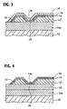
- a resistor film 14 lies on the electrodes 12, 12' and the insulating surface 10a of the substrate 10 in the heating zones 20. Tantalum is a preferred resistor material in view of adequateness of its volume resistivity and excellence in heat resistance.
- the resistor film 14 is deposited after patterning the electrodes 12, 12' over substantially the entire surface area of the thermal head, and by a photolithography process the resistor film is selectively removed in areas widthways between the rectangularly elongate electrodes 12, 12'. As the result, the resistor film 14 continuously covers the electrodes 12, 12' and the insulating surface 10a in the heating zones 20.
- the resistor film existing in each heating zone 20, indicated at 14a, serves as a heating resistor.
- a protective layer 16 which is formed by anodic oxidation of a surface layer of the resistor film 14.
- a suitable voltage is applied between the common electrode 12 and any of the selective electrodes 12' a current flows in the resistor film 14, and in the heating zone 20 where the electrodes are absent the resistor film 14a generates heat.
- a fraction of ink existing just above the heating zone 20 is heated to boil and produce a bubble, and the bubble forces a droplet of ink to spout from an orifice (not shown) above the heating zone 20 toward a recording paper.
- the heat generated in the heating zone 20 is directly transferred to a thermographic paper or a heat-sensitive ribbon.
- the oxide layer 10a on the surface of the substrate 10 provides heat insulation as well as electrical insulation.
- both the conductor film (12) and the resistor film (14) are usually deposited by sputtering techniques. In this invention only two sputtering operation are needed since the protective layer 16 is formed by anodic oxidation of the resistor film 14.
- the patterning of both the conductor film (12) and the resistor film (14) can be performed by conventional photolithography processes.
- the resistor film 14 It is preferable to deposit the resistor film 14 by a bias sputtering method. This is firstly because of fining of the individual grains of the polycrystalline structure of the deposited resistor film. Furthermore, the biasing causes the atoms of the inert gas such as argon gas used as the discharging atmosphere to intrude into the deposited polycrystal of resistor, and in operation of the thermal head, particularly in the case of continuous operation, the inert gas atoms in the resistor film 14 suppress the diffusion of oxygen from the anodically oxidized layer 16 into the resistor 14a in the heating zones 20 and consequently prevent a rise in the resistance of the resistor 14a. Therefore, the thermal head long maintains good printing quality and prolongs its service life.
- the inert gas such as argon gas used as the discharging atmosphere
- the effect of suppressing the diffusion of oxygen is appreciable when the biasing power is 10%, or above, of the sputtering power.
- the biasing power exceeds 50% of the sputtering power an excessive increase in the amount of the inert gas atoms in the resistor film 14 augments strains in the resistor film and may cause peeling of the resistor film from the underlying electrodes or the substrate surface during continuous operation of the thermal head.
- This example illustrates the fabrication of the thermal head shown in Figs. 1 and 2.
- the thermally oxidized insulating layer 10a had a thickness of 1.35 ⁇ m.
- the electrodes 12, 12' were formed by depositing an aluminum film on the insulating surface 10a of the substrabe 10 by a sputtering method to a thickness of 0.5 ⁇ m and then patterning the aluminum film by a photolithography process.
- As an etching liquid an aqueous mixed solution of phosphoric acid, nitric acid, acetic acid and ammonium fluoride was used.
- a bias sputtering method a tantalum film (resistor film 14) was deposited to a thickness of 0.25 ⁇ m.
- the sputtering gas was argon gas at 0.5 Pa.
- the sputtering power was 1000 W, and the biasing power applied to the silicon substrate 10 was 300 W.
- the deposited tantalum film was selectively removed by photolithography to form the resistor pattern 14 shown in Fig. 1.
- a surface layer of the patterned resistor film 14 was anodically oxidized in 0.1% aqueous solution of phosphoric acid by application of a voltage of 147 V between the resistor film 14 which was made anode and a counter electrode.
- the anodic oxidation was performed until the thickness of the resultant Ta2O5 layer, viz. protective layer 16, reached 0.3 ⁇ m.
- the thickness of the unoxidized tantalum film 14 was 0.1 ⁇ m.
- the protective layer 16 formed by anodic oxidation is a stoichiometric Ta2O5 layer having a very tight structure. Therefore, the thickness of the protective layer 16 can be made very thin to the extent of about 0.3 ⁇ m. For this reason the thermal head can be driven at a high speed of 20 kHz or above, and power consumpution becomes low. In the thermal head of this example, the minimum input power to each heating zone 20 for producing a bubble of ink was 650 W/mm2, which is a relatively low value.
- the object of anodic oxidation is only the resistor material, which is preferably Ta. Therefore, the anodic oxidation can be performed under the conditions optimum for that resistor material. Furthermore, the electrodes 12, 12' and the heating zones 20 are entirely covered by the resistor film 14 without discontinuity in the resistor film itself or the protective layer 16. Therefore, this thermal head is remarkably improved in durability.
- the thermal head of Example 1 exhibited durability of the order of 107 pulses, which means about 10 times improvement over a known thermal head having two different protective layers formed by anodic oxidation of an electrode material and a resistor material.
- the electrode material is not limited to aluminum. If desired it is possible to use a different material such as copper, aluminum-copper alloy or aluminum-silicon alloy. Tantalum is preferred as the resistor material, but if desired it is possible to make a selection from different materials such as tantalum-aluminum alloys, tantalum nitride, titanium and its alloys and compounds, and niobium and its alloys and compounds.
- a thermal head for ink-jet printers it is preferable to overlay the anodically oxidized protective layer 16 with a cavitation resistant layer 18 for the purpose of further enhancing the durability of the thermal head by protecting the heating zones 20 from damages by repeated cavitation induced by rupture of bubbles in the ink.
- Tantalum or titanium is preferred as the material of the cavitation resistant layer 18, and this layer 18 can be formed by a sputtering method.
- the cavitation resistant layer 18 of Ta or Ti is a conductor layer, but there is no possibility of electrical connection of this layer 18 with the electrodes 12, 12' or the resistor film 14 because of the existence of the dielectric oxide layer 16.
- the cavitation-resistant layer 18 of Ta or Ti has a thickness of from 0.2 to 0.8 ⁇ m.
- the cavitation resistant layer (Ta) 18 of such thickness was added to the thermal head of Example 1, the durability improved more than 5 times. If the cavitation resistant layer 18 is made too thick, the strength of adhesion of this layer 18 to the underlying layer lowers because of augmented strains in the layer 18.
- the optimum thickness of the cavitation resistant layer 18 is about 0.5 ⁇ m. When the thermal head of Example 1 was provided with the tantalum layer 18 of such a thickness the durability reached the order of 108 pulses.
- the surface of the insulating oxide layer 10a of the silicon substrate 10 becomes a somewhat rough surface by the influence of the etching liquid used in the photolithographic process to form the electrodes 12, 12'.
- the roughening of that surface might result in unevenness of the thickness of the resistor film 14a in each heating zone 20, and unevenness of the thickness will become a cause of failure of the heating zone 20 by concentration of current. Therefore, as shown in Fig. 4, it is also preferable to overlay the insulating oxide layer 10a on the surface of the silicon substrate 10 with another insulating layer 22 which is stable or resistant to the acidic etching liquid.
- a preferred material of the insulating layer 22 is silicon nitride.
- a silicon nitride layer can be deposited on the silicon oxide layer 10a by either a chemical vapor deposition (CVD) process or sputtering.
- the insulating layer 22 of silicon nitride has a thickness of about 1 ⁇ m. It is possible to use a different material such as tantalum pentoxide instead of silicon nitride.
- each heating zone 20 of a thermal head according to the invention there is some distribution of heat generation (amounts of heat generated per unit area), and it has been found that the distribution of heat generation depends strongly on the shape of the resistor film 14 in and in the vicinity of the heating zone 20.
- W1 width of the resistor film 14 over a terminal region of each electrode 12, 12' in the vicinity of the heating zone 20
- W2 width of the terminal region of each electrode 12, 12'
- W3 width of the resistor film 14a in the heating zone 20
- L length of the heat generating zone 20
- ⁇ L length of an edge region where the width of the resistor film 14 continuously changes from W1 to W3.
- Fig. 5 shows a good example of the resistor film shape.
- W1 was 72 ⁇ m.
- W2 was 64 ⁇ m
- W3 was 66 ⁇ m
- L was 60 ⁇ m
- ⁇ L was 3 ⁇ m.
- the ratio of P max to P o can be taken as an indication of the distribution of heat generation. If P max /P o is close to 1.0, it is presumable that the distribution of heat generation in the heating zone is close to uniformity. Testing of thermal head samples variously different in the resistor shape has proved that the durability of the thermal head is not significantly affected by uneven distributions of heat generation insofar as P max /P o is not greater than 2.0. Therefore, it is desirable that P max /P o is not greater than 2.0.
- the resistor film 14 is patterned so as to meet at least the following conditions (1) and (2).
- the following conditions (3), (4) and (5) are also met.
- W1/W2 was 1.13
- W3/W1 was 0.92
- ⁇ L/L was 0.05. That is, this sample met the conditions (3), (4) and (5) as well as the conditions (1) and (2).
- the distribution of heat generation was calculated by a simulation based on the Laplace's equation relating to potential distribution in a resistor.
- input voltage was 5.8 V
- the thickness of the resistor film (unoxidized part) was 0.1 ⁇ m
- the resistivity of the resistor was 1.55 ⁇ m.
- the obtained distribution of heat generation is shown in Fig. 6 in which only a lower-left quarter of Fig. 5 is enlarged since the resistor shape in Fig. 5 has symmetry with respect to both a longitudinal center axis and a widthwise center axis.
- the amounts of generated heat were 600-800 W/mm2 in the region A, 400-600 W/mm2 in the region B, 200-400 W/mm2 in the region C and 0-200 W/mm2 in the region D, and P max /P o was 1.19. That is, in this case heat generation does not peak in the region around the angled corner T. Therefore, this thermal head sample is fairly high in withstand voltage.
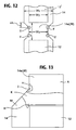
- Fig. 10 shows another good example of the resistor shape in and in the vicinity of a heating zone 20.
- W1 was 72 ⁇ m
- W2 was 64 ⁇ m
- W3 was 72 ⁇ m
- L was 60 ⁇ m. That is, W1/W2 was 1.13
- W3 was equal to w1, and ⁇ L was 0.
- This sample met the conditions (1) and (2) but did not meet the condition (3).
- a simulation of the distribution of heat generation gave the result shown in Fig. 11 which is an enlargement of a lower-left quarter of the resistor shape of Fig. 10.
- the simulation employed the same conditions as in the simulation of the sample of the resistor shape of Fig. 5.
- the amoutns of generated heat were 600-800 W/mm2 in the region A, 200-600 W/mm2 in the region E, 800-1400 W/mm2 in the region F and 0-200 W/mm2 in the region G, and P max /P o was 1.75.
- the resistor film 14 had an entirely uniform width, and hence heat generation peaked in the region F near an edge corner of each electrode 12, 12', but P max /P o still remained below 2.0.
- Fig. 12 shows an undesirable example of the resister shape.
- W1 was 96 ⁇ m
- W2 was 64 ⁇ m
- W3 was 64 ⁇ m
- L was 60 ⁇ m
- ⁇ L was 16 ⁇ m. That is, W1/W2 was 1.50, which means that the condition (2) was not met.
- the simulation employed the same conditions as in the simulation with respect to the resistor shape of Fig. 5.
- the simulation gave the result shown in Fig. 13 which is an enlargement of a lower-left quarter of the resistor shape of Fig. 12.
- the amounts of generated heat were 600-800 W/mm2 in the region A, 800-1400 W/mm2 in the regions H, above 1400 W/mm2 in the region J, 200-600 W/mm2 in the region K and 0-200 W/mm2 in the region M, and P max /P o was 2.66.
- heat generation strongly peaks in the region J around each of the angled corners T (indicated in Fig. 12) of the resistor film 14a in the heating zone. Therefore, the resistor film in the regions J experiences strong and repeated heat shocks during long operation of the thermal head, and consequently breaking of the resistor occurs in these regions J.
- the samples Nos. 1, 3, 4 and 5 met not only the conditions (1) and (2) but also the conditions (3), (4) and (5). In these samples P max /P o was fairly close to 1.0, and these samples were relatively high in breaking voltage.
- the samples Nos. 2 and 6 met the conditions (1) and (2) but did not meet one of the conditions (3), (4) and (5). In these samples P max /P o became relatively high but still remained below 2.0.
- the samples Nos. 7, 8 and 9 did not meet the condition (2). In these samples P max /P o exceeded 2.00, and these samples were considerably low in breaking voltage.
Landscapes
- Particle Formation And Scattering Control In Inkjet Printers (AREA)
- Non-Adjustable Resistors (AREA)
Applications Claiming Priority (10)
| Application Number | Priority Date | Filing Date | Title |
|---|---|---|---|
| JP266815/93 | 1993-10-26 | ||
| JP26681593 | 1993-10-26 | ||
| JP5698494A JP2738293B2 (ja) | 1993-10-26 | 1994-03-28 | サーマルヘッド |
| JP56984/94 | 1994-03-28 | ||
| JP6145006A JP2606139B2 (ja) | 1994-06-27 | 1994-06-27 | サーマルヘッドの製造方法 |
| JP14500294A JPH081979A (ja) | 1994-06-27 | 1994-06-27 | サーマルヘッド |
| JP145007/94 | 1994-06-27 | ||
| JP145002/94 | 1994-06-27 | ||
| JP14500794A JPH081975A (ja) | 1994-06-27 | 1994-06-27 | サーマルヘッド |
| JP145006/94 | 1994-06-27 |
Publications (3)
| Publication Number | Publication Date |
|---|---|
| EP0649748A2 true EP0649748A2 (fr) | 1995-04-26 |
| EP0649748A3 EP0649748A3 (fr) | 1997-01-22 |
| EP0649748B1 EP0649748B1 (fr) | 1999-04-14 |
Family
ID=27523325
Family Applications (1)
| Application Number | Title | Priority Date | Filing Date |
|---|---|---|---|
| EP19940116818 Expired - Lifetime EP0649748B1 (fr) | 1993-10-26 | 1994-10-25 | Tête thermique pour imprimantes |
Country Status (2)
| Country | Link |
|---|---|
| EP (1) | EP0649748B1 (fr) |
| DE (1) | DE69417835T2 (fr) |
Cited By (4)
| Publication number | Priority date | Publication date | Assignee | Title |
|---|---|---|---|---|
| FR2769260A1 (fr) * | 1997-10-02 | 1999-04-09 | Asahi Optical Co Ltd | Tete thermique et son utilisation dans une imprimante a transfert d'encre |
| US7559630B2 (en) | 2006-03-22 | 2009-07-14 | Lexmark International, Inc. | Substantially planar fluid ejection actuators and methods related thereto |
| CN101945768B (zh) * | 2007-07-26 | 2012-09-26 | 惠普开发有限公司 | 加热元件 |
| CN115588546A (zh) * | 2021-07-06 | 2023-01-10 | 上海傲睿科技有限公司 | 一种流体喷射设备及其制作方法 |
Families Citing this family (1)
| Publication number | Priority date | Publication date | Assignee | Title |
|---|---|---|---|---|
| JP7715553B2 (ja) * | 2021-07-08 | 2025-07-30 | ローム株式会社 | サーマルプリントヘッドの製造方法 |
Family Cites Families (4)
| Publication number | Priority date | Publication date | Assignee | Title |
|---|---|---|---|---|
| US4535343A (en) * | 1983-10-31 | 1985-08-13 | Hewlett-Packard Company | Thermal ink jet printhead with self-passivating elements |
| EP0251036B1 (fr) * | 1986-06-25 | 1991-05-08 | Kabushiki Kaisha Toshiba | Tête thermique |
| US4956653A (en) * | 1989-05-12 | 1990-09-11 | Eastman Kodak Company | Bubble jet print head having improved multi-layer protective structure for heater elements |
| JP3210454B2 (ja) * | 1992-11-20 | 2001-09-17 | 旭テック株式会社 | 車両用ホイールの鋳造装置 |
-
1994
- 1994-10-25 DE DE1994617835 patent/DE69417835T2/de not_active Expired - Fee Related
- 1994-10-25 EP EP19940116818 patent/EP0649748B1/fr not_active Expired - Lifetime
Cited By (10)
| Publication number | Priority date | Publication date | Assignee | Title |
|---|---|---|---|---|
| FR2769260A1 (fr) * | 1997-10-02 | 1999-04-09 | Asahi Optical Co Ltd | Tete thermique et son utilisation dans une imprimante a transfert d'encre |
| US6345886B1 (en) | 1997-10-02 | 2002-02-12 | Asahi Kogaku Kogyo Kabushiki Kaisha | Thermal head and ink transfer printer using same |
| GB2329872B (en) * | 1997-10-02 | 2002-02-13 | Asahi Optical Co Ltd | Thermal line head and ink transfer printer using same |
| US6428150B1 (en) | 1997-10-02 | 2002-08-06 | Asahi Kogaku Kogyo Kabushiki Kaisha | Thermal head and ink transfer printer using same |
| US6460975B2 (en) | 1997-10-02 | 2002-10-08 | Asahi Kogaku Kogyo Kabushiki Kaisha | Thermal head and ink transfer printer using same |
| US6485129B2 (en) | 1997-10-02 | 2002-11-26 | Asahi Kogaku Kogyo Kabushiki Kaisha | Thermal head and ink transfer printer using same |
| US6517194B2 (en) | 1997-10-02 | 2003-02-11 | Pentax Corporation | Thermal head and ink transfer printer using same |
| US7559630B2 (en) | 2006-03-22 | 2009-07-14 | Lexmark International, Inc. | Substantially planar fluid ejection actuators and methods related thereto |
| CN101945768B (zh) * | 2007-07-26 | 2012-09-26 | 惠普开发有限公司 | 加热元件 |
| CN115588546A (zh) * | 2021-07-06 | 2023-01-10 | 上海傲睿科技有限公司 | 一种流体喷射设备及其制作方法 |
Also Published As
| Publication number | Publication date |
|---|---|
| EP0649748B1 (fr) | 1999-04-14 |
| EP0649748A3 (fr) | 1997-01-22 |
| DE69417835T2 (de) | 1999-08-19 |
| DE69417835D1 (de) | 1999-05-20 |
Similar Documents
| Publication | Publication Date | Title |
|---|---|---|
| EP0140611B1 (fr) | Tête d'impression thermique à jet d'encre | |
| CA1275854C (fr) | Tete d'impression thermique a jet d'encre et sa methode de fabrication | |
| EP0768182B1 (fr) | Méthode de fabrication d'une tête d'enregistrement par jet d'encre, tête d'enregistrement par jet d'encre fabriquée par cette méthode et appareil d'enregistrement par jet d'encre équipé avec une telle tête | |
| EP2177360B1 (fr) | Procédé de fabrication d'un dispositif d'éjection de microfluide possédant une pellicule chauffante a résistance élevée. | |
| KR860000599B1 (ko) | 더어멀 헤드(thermal head)와 이것의 제조방법 | |
| US6950117B2 (en) | Thermal head | |
| JPS62202741A (ja) | 液体噴射記録ヘツドの作成方法 | |
| US6042221A (en) | Ink-jet recording head and ink-jet recording apparatus | |
| EP0649748B1 (fr) | Tête thermique pour imprimantes | |
| US20050174502A1 (en) | Thermal head including Si substrate and method for manufacturing the same | |
| JP2738293B2 (ja) | サーマルヘッド | |
| KR20030076372A (ko) | 서멀 헤드 | |
| JP2606139B2 (ja) | サーマルヘッドの製造方法 | |
| JP3127647B2 (ja) | 熱制御型インクジェット記録素子 | |
| JP2727989B2 (ja) | サーマルヘッドの製造方法 | |
| US20050052501A1 (en) | Heater for inkjet printer head and method for production thereof | |
| JPH07153603A (ja) | インクジェット用発熱抵抗体の製造方法及びインクジェットプリンタ | |
| JPH11216865A (ja) | サーマルインクジェットプリントヘッド及びその製造方法 | |
| JPH09118018A (ja) | インクジェット記録ヘッド用基板の作製方法 | |
| JP2748858B2 (ja) | プリンタ用サーマルヘッドおよびその製造方法 | |
| JPH0528183B2 (fr) | ||
| JPH1191111A (ja) | インクジェット記録ヘッド | |
| JPH06340103A (ja) | サーマルヘッド | |
| JP3225317B2 (ja) | サーマルプリントヘッドおよびその製造方法 | |
| JPS6151359A (ja) | サ−マルヘツド |
Legal Events
| Date | Code | Title | Description |
|---|---|---|---|
| PUAI | Public reference made under article 153(3) epc to a published international application that has entered the european phase |
Free format text: ORIGINAL CODE: 0009012 |
|
| AK | Designated contracting states |
Kind code of ref document: A2 Designated state(s): DE GB IT |
|
| PUAL | Search report despatched |
Free format text: ORIGINAL CODE: 0009013 |
|
| AK | Designated contracting states |
Kind code of ref document: A3 Designated state(s): DE GB IT |
|
| 17P | Request for examination filed |
Effective date: 19961212 |
|
| GRAG | Despatch of communication of intention to grant |
Free format text: ORIGINAL CODE: EPIDOS AGRA |
|
| 17Q | First examination report despatched |
Effective date: 19980312 |
|
| GRAG | Despatch of communication of intention to grant |
Free format text: ORIGINAL CODE: EPIDOS AGRA |
|
| GRAG | Despatch of communication of intention to grant |
Free format text: ORIGINAL CODE: EPIDOS AGRA |
|
| GRAH | Despatch of communication of intention to grant a patent |
Free format text: ORIGINAL CODE: EPIDOS IGRA |
|
| GRAH | Despatch of communication of intention to grant a patent |
Free format text: ORIGINAL CODE: EPIDOS IGRA |
|
| GRAA | (expected) grant |
Free format text: ORIGINAL CODE: 0009210 |
|
| AK | Designated contracting states |
Kind code of ref document: B1 Designated state(s): DE GB IT |
|
| REF | Corresponds to: |
Ref document number: 69417835 Country of ref document: DE Date of ref document: 19990520 |
|
| PLBE | No opposition filed within time limit |
Free format text: ORIGINAL CODE: 0009261 |
|
| STAA | Information on the status of an ep patent application or granted ep patent |
Free format text: STATUS: NO OPPOSITION FILED WITHIN TIME LIMIT |
|
| 26N | No opposition filed | ||
| REG | Reference to a national code |
Ref country code: GB Ref legal event code: IF02 |
|
| PGFP | Annual fee paid to national office [announced via postgrant information from national office to epo] |
Ref country code: DE Payment date: 20061019 Year of fee payment: 13 |
|
| PGFP | Annual fee paid to national office [announced via postgrant information from national office to epo] |
Ref country code: GB Payment date: 20061025 Year of fee payment: 13 |
|
| PGFP | Annual fee paid to national office [announced via postgrant information from national office to epo] |
Ref country code: IT Payment date: 20061031 Year of fee payment: 13 |
|
| GBPC | Gb: european patent ceased through non-payment of renewal fee |
Effective date: 20071025 |
|
| PG25 | Lapsed in a contracting state [announced via postgrant information from national office to epo] |
Ref country code: DE Free format text: LAPSE BECAUSE OF NON-PAYMENT OF DUE FEES Effective date: 20080501 |
|
| PG25 | Lapsed in a contracting state [announced via postgrant information from national office to epo] |
Ref country code: GB Free format text: LAPSE BECAUSE OF NON-PAYMENT OF DUE FEES Effective date: 20071025 |
|
| PG25 | Lapsed in a contracting state [announced via postgrant information from national office to epo] |
Ref country code: IT Free format text: LAPSE BECAUSE OF NON-PAYMENT OF DUE FEES Effective date: 20071025 |