EP0650115A1 - Multiplieur capable de calculer en modes précision double, précision simple, produit scalaire et de multiplier des nombres complexes - Google Patents
Multiplieur capable de calculer en modes précision double, précision simple, produit scalaire et de multiplier des nombres complexes Download PDFInfo
- Publication number
- EP0650115A1 EP0650115A1 EP94116565A EP94116565A EP0650115A1 EP 0650115 A1 EP0650115 A1 EP 0650115A1 EP 94116565 A EP94116565 A EP 94116565A EP 94116565 A EP94116565 A EP 94116565A EP 0650115 A1 EP0650115 A1 EP 0650115A1
- Authority
- EP
- European Patent Office
- Prior art keywords
- multiplicand
- booth
- inputted
- word
- multiplier
- Prior art date
- Legal status (The legal status is an assumption and is not a legal conclusion. Google has not performed a legal analysis and makes no representation as to the accuracy of the status listed.)
- Granted
Links
Images

Classifications
-
- G—PHYSICS
- G06—COMPUTING OR CALCULATING; COUNTING
- G06F—ELECTRIC DIGITAL DATA PROCESSING
- G06F7/00—Methods or arrangements for processing data by operating upon the order or content of the data handled
- G06F7/38—Methods or arrangements for performing computations using exclusively denominational number representation, e.g. using binary, ternary, decimal representation
- G06F7/48—Methods or arrangements for performing computations using exclusively denominational number representation, e.g. using binary, ternary, decimal representation using non-contact-making devices, e.g. tube, solid state device; using unspecified devices
- G06F7/52—Multiplying; Dividing
- G06F7/523—Multiplying only
- G06F7/53—Multiplying only in parallel-parallel fashion, i.e. both operands being entered in parallel
- G06F7/5324—Multiplying only in parallel-parallel fashion, i.e. both operands being entered in parallel partitioned, i.e. using repetitively a smaller parallel parallel multiplier or using an array of such smaller multipliers
-
- G—PHYSICS
- G06—COMPUTING OR CALCULATING; COUNTING
- G06F—ELECTRIC DIGITAL DATA PROCESSING
- G06F7/00—Methods or arrangements for processing data by operating upon the order or content of the data handled
- G06F7/38—Methods or arrangements for performing computations using exclusively denominational number representation, e.g. using binary, ternary, decimal representation
- G06F7/48—Methods or arrangements for performing computations using exclusively denominational number representation, e.g. using binary, ternary, decimal representation using non-contact-making devices, e.g. tube, solid state device; using unspecified devices
- G06F7/4806—Computations with complex numbers
- G06F7/4812—Complex multiplication
-
- G—PHYSICS
- G06—COMPUTING OR CALCULATING; COUNTING
- G06F—ELECTRIC DIGITAL DATA PROCESSING
- G06F7/00—Methods or arrangements for processing data by operating upon the order or content of the data handled
- G06F7/38—Methods or arrangements for performing computations using exclusively denominational number representation, e.g. using binary, ternary, decimal representation
- G06F7/48—Methods or arrangements for performing computations using exclusively denominational number representation, e.g. using binary, ternary, decimal representation using non-contact-making devices, e.g. tube, solid state device; using unspecified devices
- G06F7/52—Multiplying; Dividing
- G06F7/523—Multiplying only
- G06F7/533—Reduction of the number of iteration steps or stages, e.g. using the Booth algorithm, log-sum, odd-even
- G06F7/5334—Reduction of the number of iteration steps or stages, e.g. using the Booth algorithm, log-sum, odd-even by using multiple bit scanning, i.e. by decoding groups of successive multiplier bits in order to select an appropriate precalculated multiple of the multiplicand as a partial product
- G06F7/5336—Reduction of the number of iteration steps or stages, e.g. using the Booth algorithm, log-sum, odd-even by using multiple bit scanning, i.e. by decoding groups of successive multiplier bits in order to select an appropriate precalculated multiple of the multiplicand as a partial product overlapped, i.e. with successive bitgroups sharing one or more bits being recoded into signed digit representation, e.g. using the Modified Booth Algorithm
- G06F7/5338—Reduction of the number of iteration steps or stages, e.g. using the Booth algorithm, log-sum, odd-even by using multiple bit scanning, i.e. by decoding groups of successive multiplier bits in order to select an appropriate precalculated multiple of the multiplicand as a partial product overlapped, i.e. with successive bitgroups sharing one or more bits being recoded into signed digit representation, e.g. using the Modified Booth Algorithm each bitgroup having two new bits, e.g. 2nd order MBA
-
- G—PHYSICS
- G06—COMPUTING OR CALCULATING; COUNTING
- G06F—ELECTRIC DIGITAL DATA PROCESSING
- G06F7/00—Methods or arrangements for processing data by operating upon the order or content of the data handled
- G06F7/38—Methods or arrangements for performing computations using exclusively denominational number representation, e.g. using binary, ternary, decimal representation
- G06F7/48—Methods or arrangements for performing computations using exclusively denominational number representation, e.g. using binary, ternary, decimal representation using non-contact-making devices, e.g. tube, solid state device; using unspecified devices
- G06F7/544—Methods or arrangements for performing computations using exclusively denominational number representation, e.g. using binary, ternary, decimal representation using non-contact-making devices, e.g. tube, solid state device; using unspecified devices for evaluating functions by calculation
- G06F7/5443—Sum of products
-
- G—PHYSICS
- G06—COMPUTING OR CALCULATING; COUNTING
- G06F—ELECTRIC DIGITAL DATA PROCESSING
- G06F2207/00—Indexing scheme relating to methods or arrangements for processing data by operating upon the order or content of the data handled
- G06F2207/38—Indexing scheme relating to groups G06F7/38 - G06F7/575
- G06F2207/3804—Details
- G06F2207/3808—Details concerning the type of numbers or the way they are handled
- G06F2207/3812—Devices capable of handling different types of numbers
- G06F2207/382—Reconfigurable for different fixed word lengths
Definitions
- the present invention relates to a multiplier, which is particularly used in a parallel multiplier.
- FIGS. 1A and 1B show a conventional parallel multiplier using Booth's algorithm.
- reference numeral 1 is a Booth's decoder
- 2 a Booth's selector
- 3 a parallel adding circuit for adding partial products.
- FIG. 2 shows an example of a circuit forming the Booth's decoder 1 of FIG. 1A.
- reference numeral 4 is an NAND gate
- 5 an NOR gate
- 6 an OR gate
- 7 an AND gate
- 8 an inverter.
- FIG. 3 shows an example of a circuit forming the Booth's selector 2 of FIG. 1A.
- reference numeral 9 is an exclusive NOR gate.
- the parallel adding circuit which is disclosed in Japanese Patent Application KOKAI Publication No. 63-55627, can be used.
- Booth's algorithm is algorithm for multiplying a multiplier X and a multiplicand Y, which are expressed by twos complement, together at high speed as shown in equations (1) and (2).
- equation (3) if a value of the multiplicand Y is decoded every three bits by the decoder 1, and each bit of the multiplier X is selected by the selector 2 in accordance with the decoding result, a partial products Pm is generated.
- the calculating speed can be increased.
- Multiplier X -2 n-1 x n-1 + 2 n-2 x n-2 + ... + 2x1 + x0 (1)
- Multiplicand Y 2 n-1 y n-1 + 2 n-2 y n-2 + ...
- an LSI which is mounted on the apparatus
- an LSI whose consumption of electrical power is low is required so as to prolong a life of a battery.
- the digital processing is essential, and an LSI for digital signal processing, that is, a digital signal processor (DSP) is mounted on the above apparatus.
- DSP digital signal processor
- the principle of the operation of the digital signal processor is substantially the same as that of a general purpose microprocessor. Due to this, the more the processing becomes complicated, the more the processing time is increased. However, since the processing time has its upper limit, a frequency of an operation clock must be increased in the portable data communication apparatus in which a real time operation is required. However, if the clock frequency is increased, the consumption of electrical power is increased.
- the parallel process is that a plurality of processings are executed in parallel. An amount of processing within the unit time can be increased without increasing the clock frequency.
- the basic calculation of the digital signal processing is an operation in which the calculation of the sum of products, that is, the multiplied results are cumulatively added. Therefore, both the multiplier and the adder are built in the digital signal processor.
- the above-mentioned convention multiplier can multiply only a pair of data at one time. Due to this, for executing the calculation of the sum of products at a double speed by the parallel processing, two multipliers must be built in the digital signal processor. Also, for cumulatively adding the multiplied results, at least two adders must be built therein.
- the results, which are separately added must be added. Due to this, one more adder must be built in the digital signal processor, or two sets of registers (accumulators) for saving the results, which are separately added, must be prepared.
- a compiler having an optimization function is indispensable for using such a paralleled architecture.
- an object conversion efficiency of the compiler does not suffice, the programming of the digital signal processor is executed by use of a common assembler. Due to this, the paralleled architecture applies an optimization load to the programmer, and efficiency of developing the software is dropped.
- the circuit scale of the double precision multiplier is four times as large as that of the single precision multiplier, an area occupacy ratio of the double precision multiplier to the LSI is increased.
- the conventional multiplier is used, the plurality of the multipliers are needed in parallel processing for the above-mentioned reason. Therefore, such multipliers are not suitable in practical use.
- the conventional multiplier has the following disadvantages.
- the provision of the parallel processing enlarges the circuit scale of the digital signal processor.
- the paralleled architecture applies an optimization load to the programmer.
- an object of the present invention is to provide a multiplier, which can multiply a plurality of pairs of data at one time without increase in the consumption of electrical power and increase in the circuit scale.
- a multiplier using Booth's algorithm comprising a first Booth's decoder for inputting a host word of a multiplicand thereto; a second Booth's decoder for inputting a lower word of the multiplicand thereto; multiplicand dividing means for inputting the most significant bit of the lower word of the multiplicand or "0" to an input terminal of the least significant bit of the first Booth's decoder; zeroising means for replacing a part of partial products with "0"; and bit extension means for replacing the other part of the partial products with one bit of the partial products of lower bits than the other part of the partial products.
- the most significant bit of the lower word of the multiplicand is inputted to an input terminal of the most significant bit of the first Booth's decoder by the multiplicand dividing means, and the zeroising means and the bit extension means are not functioned, whereby multiplying a single precision or that of a double precision.
- a multiplier using Booth's algorithm comprising: a first Booth's decoder for inputting a host word of a multiplicand thereto; a second Booth's decoder for inputting a lower word of the multiplicand thereto; multiplicand complementing means for inputting "0" or "1" to an input terminal of the least significant bit of the second Booth's decoder, and for inputting the lower word of the multiplicand or the reversed signal to the second Booth's decoder; multiplicand dividing means for inputting the most significant bit of the lower word of the multiplicand or "0" to the input terminal of the least significant bit of the first Booth's decoder; zeroising means for replacing a part of partial products with "0"; and bit extension means for replacing the other part of the partial products with one bit of the partial products of lower bits than the other part of the partial products.
- a multiplier using Booth's algorithm comprising: a first Booth's decoder for inputting a host word of a multiplicand thereto; a second Booth's decoder for inputting a lower word of the multiplicand thereto; multiplicand dividing means for inputting the most significant bit of the lower word of the multiplicand or "1" to the input terminal of the least significant bit of the first Booth's decoder; reversing means for inputting the host word of the multiplicand or the reversed signal to the first Booth's decoder; zeroising means for replacing a part of partial products with "0"; and bit extension means for replacing the other part of the partial products with one bit of the partial products of lower bits than the other part of the partial products.
- a and b are inputted to the host word of the multiplier and the lower word of the multiplier, respectively
- c and d are inputted to the host word of the multiplicand and the lower word of the multiplicand, respectively
- the host word of the multiplicand is inputted to the first Booth's decoder by the multiplicand complementing means
- "0" is inputted to the input terminal of the least significant bit of the first Booth's decoder by the multiplicand dividing means
- the part of the partial products generated in the multiplier is zeroising, and the other part of the partial products is replaced with one bit of the partial products lower than the other part of the partial products, whereby the plurality of pairs of data can be multiplied by one multiplier.
- multiplication of a plurality of pairs of data can be performed at one time, not only normal multiplication but also the double precision multiplication, the inner product of the vector, and the complex multiplication can be performed by one multiplier.
- the multiplier of the present invention is incorporated into the processor, the above all calculations can be performed by a single machine cycle, so that the number of steps of program can be reduced. Particularly, the number of steps can be reduced to about 1/2 of the conventional case in the signal processing program in which the calculation of the sum of product is mainly performed.
- the machine cycle is set to be longer than the conventional case, and the consumption of the electrical power of the entire processor can be reduced.
- the consumption of the electrical power can be reduced to about 1/2 of the conventional case.
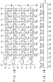
- FIGS. 4A and 4B show a multiplier of a first embodiment of the present invention.
- 1A to 1D are Booth's decoders
- 2 a Booth's selector
- 3 a parallel addition circuit for adding partial products
- 7A and 7B AND gates
- 10 a selector.
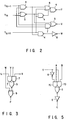
- FIG. 5 is a circuit diagram showing one example of the selector 10 used in the multiplier of the present invention.
- 5 a NOR gate
- 7C and 7D AND gates
- 8 an inverter.
- Host words Y7 to Y4 of an multiplicand are inputted to the Booth's decoders 1A and 1B. More specifically, the respective bits Y7 to Y5 of the multiplicand are inputted to the Booth's decoder 1A, the respective bits Y5 to Y4 of the multiplicand are inputted to the Booth's decoder 1B.
- the NAND circuit (multiplicand dividing means) 7A serves to input the most significant bit Y3 of the lower words Y3 to Y0 of the multiplicand or "0" to an input terminal of the least significant bit of the Booth's decoder 1B.
- a control signal S1 controls to output whether the most significant bit Y3 of the lower words of the multiplicand or "0.”
- the lower words Y3 to Y0 of the multiplicand are inputted to the Booth's decoders 1C and 1D. More specifically, the respective bits Y3 to Y1 of the multiplicand are inputted to the Booth's decoder 1C, the respective bits Y1 to Y0 of the multiplicand and "0" are inputted to the Booth's decoder 1D.
- the NAND circuit (zeroising means) 7B replaces a part of the partial products, for example, P03 to P00, P13 to P10, with "0.” In other words, if the control signal S1 is set to "0", all output signals of the NAND circuit 7B are "0", and the part of the partial products (P03 to P00, P13 to P10) are changed to "0.”
- the selector (bit extending means) 10 replaces the other part of the partial products, for example, P28 to P25 with one bit of the partial products (P24) of the lower bits. Moreover, the selector 10 replaces the other part of the partial products, for example, P38 to P35 with one bit of the partial products (P34) of the lower bits.
- each of the multiplier X and the multiplicand Y is divided to the host word and the lower word.
- (Multiplier) X X H + X L (5)
- (Multiplicand) Y Y H + Y L (6)
- a product Z can be expressed by equation (7)
- the host word X7 ⁇ 4 of the multiplier of FIG. 4 corresponds to X H
- the lower word X3 ⁇ 0 corresponds to X L
- the host word Y7 ⁇ 4 of the multiplicand of FIGS. 4A and 4B corresponds to Y H
- the lower word X3 ⁇ 0 corresponds to Y L .
- S1 is a control signal.
- input data is processed word by word, and the control signal S1 is switched, thereby making it possible to execute three types of multiplications, that is, a single precision, a double precision, and an inner product.
- the product Z can be expressed by the following equation (8).
- (Single precision) Z X H Y H (8)
- the multiplier of this embodiment performs the same operation as the conventional multiplier of FIGS. 1A and 1B.
- each selector 10 selects input data X7, X6, X5, and X4, and each of the AND gates 7A and 7B directly outputs the level of the other input signal since the control signal S1, which is inputted to one input terminal, is "1."
- the multiplier of this embodiment performs the same operation as the conventional multiplier of FIGS. 1A and 1B. Due to this, if X7 ⁇ 0 and Y7 ⁇ 0 are set to 8 bit double precision data, respectively, the multiplication result (output data) of the double precision can be obtained.
- equation (7) the multiplication is performed in the following condition (equation (9)).
- Z a1b0 + a1b1 + a0b0 + a0b1 (10)
- equation (11) can be obtained and the inner products of the vectors and are calculated.
- the AND gates 7A and 7B output "0", and the selector 10 outputs an sign bit X3 of the lower word X L of the multiplier.
- the above point means that no overflow is generated in the calculation of the inner product. More specifically, in general, there is possibility that overflow will be generated one bit in the multiplication and one bit in addition. Since two multiplications and one addition are performed in the calculation of the inner product, the number of digits of the overflow is 3 bits in all.
- the sign extension of the host bit rather than the sign bit is performed by the number of bits of each of host and lower words. Therefore, if the number of bits of each word is larger than two bits, no overflow is generated.
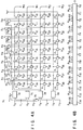
- FIGS. 6A and 6B show a multiplier of a second embodiment of the present invention.
- reference numeral 11 is an exclusive OR gate
- S2 is a control signal.
- the same reference numerals are added to the same structural elements as FIGS. 4A and 4B, and the explanation is omitted.
- the host words Y7 to Y4 of the multiplicand are inputted to the Booth's decoders 1A and 1B. More specifically, the respective bits Y7 to Y5 of the multiplicand are inputted to the Booth's decoder 1A, and the respective bits Y5 to Y4 of the multiplicand are inputted to the Booth's decoder 1B.
- the AND circuit (multiplicand dividing means) 7A serves to input the most significant bit Y3 of the lower words Y3 to Y0 of the multiplicand or "0" to the input terminal of the least significant bit of the Booth's decoder 1B.
- the control signal S1 controls whether the AND circuit 7A outputs whether the most significant bit Y3 of the lower words of the multiplicand or "0.”
- the lower words Y3 to Y0 of the multiplicand and a control signal S2 are inputted to the Booth's decoders 1C and 1D. More specifically, the respective bits Y3 to Y1 of the multiplicand are inputted to the Booth's decoder 1C, and the respective bits Y1 to Y0 of the multiplicand and the control signal S2 are inputted to the Booth's decoder 1D.
- the control signal S2 ("0" or "1" is inputted to the input terminal of the least significant bit of the Booth's decoders 1C and 1D.
- the exclusive OR gate (multiplicand complementing means) 11 has a function for inputting the lower words Y3 to Y0 of the multiplicand or the reverse signal are inputted to the Booth's decoders 1C and 1D.
- the exclusive OR gate 11 is controlled by the control signal S2.
- the AND circuit (zeroising means) 7B replaces a part of the partial products, for example, P03 to P00, P13 to P10, with "0.” In other words, if the control signal S1 is set to "0", all output signals of the AND circuit 7B are "0", and the part of the partial products (P03 to P00, P13 to P10) are changed to "0.”
- the selector (bit extending means) 10 replaces the other part of the partial products, for example, P28 to P25 with one bit of the partial products (P24) of the lower bits. Moreover, the selector 10 replaces the other part of the partial products, for example, P38 to P35 with one bit of the partial products (P34) of the lower bits.
- a real part of the product can be calculated as follow.
- equation (7) the multiplication is performed in the following condition (equation (12)).
- equation (13) the following equation (13) can be obtained.
- Z bc + b (-d) + ac + a (-d) (13) If the first and fourth terms of equation (13) are set to "0" in the multiplier, the following equation (14) can be obtained, and the real part of the product of the complex numbers F and G is calculated.
- control signal S2 is set to "1"
- the sign extension of the host bit rather than the sign bit is performed by the number of bits of each word. Therefore, if the number of bits of each word is larger than two bits, no overflow is generated.
- equation (7) the multiplication is performed in the following condition (equation (15)).
- equation (16) the following equation (16) can be obtained.
- Z ac + ad + bc + bd (16) If the first and fourth terms of equation (16) are set to "0" in the multiplier, the following equation (17) can be obtained and the imaginary part of the products of the complex numbers F and C are calculated.
- control signal S2 is set to "0"
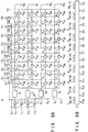
- FIGS. 7A and 7B show a multiplier of a third embodiment of the present invention.
- reference numeral 6 is an OR gate
- S2 is a control signal.
- the same reference numerals are added to the same structural elements as the multiplier of FIGS. 4 and 6, and the explanation is omitted.
- the host words Y7 to Y4 of the multiplicand are inputted to the Booth's decoders 1A and 1B. More specifically, the respective bits Y7 to Y5 of the multiplicand are inputted to the Booth's decoder 1A, and the respective bits Y5 to Y4 of the multiplicand are inputted to the Booth's decoder 1B.
- the OR circuit (multiplicand dividing means) 6 and the AND circuit (multiplicand dividing means) 7A serve to input the most significant bit Y3 of the lower words Y3 to Y0 of the multiplicand or "0" to the input terminal of the least significant bit of the Booth's decoder 1B.
- the control signals S1 and S2 control whether the AND circuit 7A outputs whether the most significant bit Y3 of the lower words of the multiplicand or "0."
- the lower words Y3 to Y0 of the multiplicand and "0" are inputted to the Booth's decoders 1C and 1D. More specifically, the respective bits Y3 to Y1 of the multiplicand are inputted to the Booth's decoder 1C, and the respective bits Y1 to Y0 of the multiplicand and "0" are inputted to the Booth's decoder 1D.
- the exclusive OR gate (multiplicand complementing means) 11 has a function for inputting the host words Y7 to Y4 of the multiplicand or the reverse signal are inputted to the Booth's decoders 1A and 1B.
- the exclusive OR gate 11 is controlled by the control signal S2.
- the AND circuit (zeroising means) 7B replaces a part of the partial products, for example, P03 to P00, P13 to P10, with "0.” In other words, if the control signal S1 is set to "0", all output signals of the AND circuit 7B are "0", and the part of the partial products (P03 to P00, P13 to P10) are changed to "0.”
- the selector (bit extending means) 10 replaces the other part of the partial products, for example, P28 to P25 with one bit of the partial products (P24) of the lower bits. Moreover, the selector 10 replaces the other part of the partial products, for example, P38 to P35 with one bit of the partial products (P34) of the lower bits.
- a real part of the product can be calculated as follow.
- equation (7) the multiplication is performed in the following condition (equation (18)).
- equation (19) the following equation (19) can be obtained.
- Z a (-d) + ac + b (-d) + bc (19) If the first and fourth terms of equation (19) are set to "0" in the multiplier, the following equation (20) can be obtained, and the real part of the products of the complex numbers F and G are calculated.
- the position of the decimal point of output data is placed between Z10 and Z9.
- the position of the decimal point of output data is placed between Z4 and Z3. If the number of bits of each word is larger than two bits, no overflow is generated.
- An imaginary part of the product can be calculated in the same manner as the embodiment of FIG. 6.
- equation (7) the multiplication is performed in the following condition (equation (15')).
- equation (16') the following equation (16') can be obtained.
- Z ac + ad + bc + bd (16') If the first and fourth terms of equation (16') are set to "0" in the multiplier, the following equation (17') can be obtained and the imaginary part of the products of the complex numbers F and C are calculated.
- control signal S2 is set to "0"
- the number of pairs of data to be multiplied is not limited to two pairs, and three or more pairs of data may be multiplied.
- the multiplier of the present invention since multiplication of a plurality of pairs of data can be performed at one time, not only normal multiplication but also the double precision multiplication, the inner product of the vector, and the complex multiplication can be performed by one multiplier.
- the above all calculations can be performed by a single machine cycle, so that the number of steps of program can be reduced.
- the number of steps can be reduced to about 1/2 of the conventional case in the signal processing program in which the calculation of the sum of product is mainly performed.
- the machine cycle is set to be longer than the conventional case, and the consumption of the electrical power of the entire processor can be reduced.
- the consumption of the electrical power can be reduced to about 1/2 of the conventional case.
Landscapes
- Engineering & Computer Science (AREA)
- Physics & Mathematics (AREA)
- General Physics & Mathematics (AREA)
- Computational Mathematics (AREA)
- Mathematical Analysis (AREA)
- Mathematical Optimization (AREA)
- Pure & Applied Mathematics (AREA)
- Theoretical Computer Science (AREA)
- Computing Systems (AREA)
- General Engineering & Computer Science (AREA)
- Complex Calculations (AREA)
Applications Claiming Priority (3)
| Application Number | Priority Date | Filing Date | Title |
|---|---|---|---|
| JP26372493A JP3637073B2 (ja) | 1993-10-21 | 1993-10-21 | 倍精度・単精度・内積演算および複素乗算が可能な乗算器 |
| JP263724/93 | 1993-10-21 | ||
| JP26372493 | 1993-10-21 |
Publications (2)
| Publication Number | Publication Date |
|---|---|
| EP0650115A1 true EP0650115A1 (fr) | 1995-04-26 |
| EP0650115B1 EP0650115B1 (fr) | 2001-03-07 |
Family
ID=17393431
Family Applications (1)
| Application Number | Title | Priority Date | Filing Date |
|---|---|---|---|
| EP94116565A Expired - Lifetime EP0650115B1 (fr) | 1993-10-21 | 1994-10-20 | Multiplieur capable de calculer en modes précision double, précision simple, produit scalaire et de multiplier des nombres complexes |
Country Status (5)
| Country | Link |
|---|---|
| US (1) | US5521856A (fr) |
| EP (1) | EP0650115B1 (fr) |
| JP (1) | JP3637073B2 (fr) |
| KR (1) | KR100305530B1 (fr) |
| DE (1) | DE69426801T2 (fr) |
Families Citing this family (14)
| Publication number | Priority date | Publication date | Assignee | Title |
|---|---|---|---|---|
| US6295599B1 (en) * | 1995-08-16 | 2001-09-25 | Microunity Systems Engineering | System and method for providing a wide operand architecture |
| US6643765B1 (en) | 1995-08-16 | 2003-11-04 | Microunity Systems Engineering, Inc. | Programmable processor with group floating point operations |
| JP3655403B2 (ja) | 1995-10-09 | 2005-06-02 | 株式会社ルネサステクノロジ | データ処理装置 |
| US5677863A (en) * | 1996-04-04 | 1997-10-14 | Hewlett-Packard Co. | Method of performing operand increment in a booth recoded multiply array |
| US5880985A (en) * | 1996-10-18 | 1999-03-09 | Intel Corporation | Efficient combined array for 2n bit n bit multiplications |
| CA2227531C (fr) * | 1997-01-20 | 2003-03-18 | Hitachi, Ltd. | Unite de traitement graphique et systeme de traitement graphique |
| JPH11134175A (ja) * | 1997-10-29 | 1999-05-21 | Toshiba Corp | 乗加減算器及び演算器 |
| JP3139466B2 (ja) | 1998-08-28 | 2001-02-26 | 日本電気株式会社 | 乗算器及び積和演算器 |
| KR100324313B1 (ko) * | 1998-11-02 | 2002-06-22 | 김영환 | n비트와n/2비트를연산하는곱셈기 |
| US6523055B1 (en) | 1999-01-20 | 2003-02-18 | Lsi Logic Corporation | Circuit and method for multiplying and accumulating the sum of two products in a single cycle |
| US6692534B1 (en) * | 1999-09-08 | 2004-02-17 | Sun Microsystems, Inc. | Specialized booth decoding apparatus |
| US20060224653A1 (en) * | 2005-04-01 | 2006-10-05 | Kimming So | Method and system for dynamic session control of digital signal processing operations |
| US8539301B2 (en) * | 2009-10-21 | 2013-09-17 | Nec Laboratories America, Inc. | Message-wise unequal error protection |
| US10528642B2 (en) * | 2018-03-05 | 2020-01-07 | International Business Machines Corporation | Multiple precision integer multiple by matrix-matrix multiplications using 16-bit floating point multiplier |
Citations (4)
| Publication number | Priority date | Publication date | Assignee | Title |
|---|---|---|---|---|
| EP0209446A1 (fr) * | 1985-07-16 | 1987-01-21 | Thomson-Csf | Multiplieur pour la multiplication de deux nombres complexes |
| EP0239899A1 (fr) * | 1986-03-31 | 1987-10-07 | Kabushiki Kaisha Toshiba | Circuit multiplieur à structure matricielle |
| US4813008A (en) * | 1986-03-31 | 1989-03-14 | Kabushiki Kaisha Toshiba | Multiplier circuit suitable for obtaining a negative product of a multiplier and a multiplicand |
| JPH04184530A (ja) * | 1990-11-20 | 1992-07-01 | Matsushita Electric Ind Co Ltd | 演算装置 |
Family Cites Families (6)
| Publication number | Priority date | Publication date | Assignee | Title |
|---|---|---|---|---|
| US4680727A (en) * | 1984-09-24 | 1987-07-14 | Rockwell International Corporation | Complex multiplier for binary two's complement numbers |
| US4754421A (en) * | 1985-09-06 | 1988-06-28 | Texas Instruments Incorporated | Multiple precision multiplication device |
| JPS63241634A (ja) * | 1987-03-30 | 1988-10-06 | Toshiba Corp | 並列型加算回路 |
| US5262976A (en) * | 1989-11-13 | 1993-11-16 | Harris Corporation | Plural-bit recoding multiplier |
| DE69032391T2 (de) * | 1989-11-13 | 1998-10-29 | Harris Corp | Mehrere Bit umkodierender Multiplizierer |
| US5420809A (en) * | 1993-11-30 | 1995-05-30 | Texas Instruments Incorporated | Method of operating a data processing apparatus to compute correlation |
-
1993
- 1993-10-21 JP JP26372493A patent/JP3637073B2/ja not_active Expired - Fee Related
-
1994
- 1994-10-20 EP EP94116565A patent/EP0650115B1/fr not_active Expired - Lifetime
- 1994-10-20 US US08/326,210 patent/US5521856A/en not_active Expired - Lifetime
- 1994-10-20 KR KR1019940026822A patent/KR100305530B1/ko not_active Expired - Fee Related
- 1994-10-20 DE DE69426801T patent/DE69426801T2/de not_active Expired - Fee Related
Patent Citations (4)
| Publication number | Priority date | Publication date | Assignee | Title |
|---|---|---|---|---|
| EP0209446A1 (fr) * | 1985-07-16 | 1987-01-21 | Thomson-Csf | Multiplieur pour la multiplication de deux nombres complexes |
| EP0239899A1 (fr) * | 1986-03-31 | 1987-10-07 | Kabushiki Kaisha Toshiba | Circuit multiplieur à structure matricielle |
| US4813008A (en) * | 1986-03-31 | 1989-03-14 | Kabushiki Kaisha Toshiba | Multiplier circuit suitable for obtaining a negative product of a multiplier and a multiplicand |
| JPH04184530A (ja) * | 1990-11-20 | 1992-07-01 | Matsushita Electric Ind Co Ltd | 演算装置 |
Non-Patent Citations (1)
| Title |
|---|
| PATENT ABSTRACTS OF JAPAN vol. 16, no. 506 (P - 1440) 20 October 1992 (1992-10-20) * |
Also Published As
| Publication number | Publication date |
|---|---|
| JP3637073B2 (ja) | 2005-04-06 |
| KR100305530B1 (ko) | 2001-11-22 |
| JPH07121354A (ja) | 1995-05-12 |
| DE69426801T2 (de) | 2001-07-19 |
| EP0650115B1 (fr) | 2001-03-07 |
| DE69426801D1 (de) | 2001-04-12 |
| US5521856A (en) | 1996-05-28 |
Similar Documents
| Publication | Publication Date | Title |
|---|---|---|
| EP3835942B1 (fr) | Systèmes et procédés de chargement de poids dans un bloc de traitement de tenseur | |
| US5880981A (en) | Method and apparatus for reducing the power consumption in a programmable digital signal processor | |
| EP0239899B1 (fr) | Circuit multiplieur à structure matricielle | |
| US6009451A (en) | Method for generating barrel shifter result flags directly from input data | |
| EP0650115A1 (fr) | Multiplieur capable de calculer en modes précision double, précision simple, produit scalaire et de multiplier des nombres complexes | |
| JP5273866B2 (ja) | 乗算器/アキュムレータ・ユニット | |
| EP1293891B2 (fr) | Processeur arithmétique accomodant différentes tailles de champ fini. | |
| EP0448367A2 (fr) | Multiplicateur numérique parallèle à grande vitesse | |
| US5343416A (en) | Method and apparatus for re-configuring a partial product reduction tree | |
| US5023827A (en) | Radix-16 divider using overlapped quotient bit selection and concurrent quotient rounding and correction | |
| US5301139A (en) | Shifter circuit for multiple precision division | |
| US4528641A (en) | Variable radix processor | |
| US5164724A (en) | Data format converters for use with digit-serial signals | |
| US5245563A (en) | Fast control for round unit | |
| US5016011A (en) | Increased performance of digital integrated circuits by processing with multiple-bit-width digits | |
| US5957999A (en) | Booth multiplier with squaring operation accelerator | |
| US5025257A (en) | Increased performance of digital integrated circuits by processing with multiple-bit-width digits | |
| US4866655A (en) | Arithmetic processor and divider using redundant signed digit | |
| US5034908A (en) | Digit-serial transversal filters | |
| US6269385B1 (en) | Apparatus and method for performing rounding and addition in parallel in floating point multiplier | |
| US4942396A (en) | To-digit-serial converters for systems processing data in digit-serial format | |
| US5034909A (en) | Digit-serial recursive filters | |
| US6144979A (en) | Method and apparatus for performing multiply operation of floating point data in 2-cycle pipeline scheme | |
| KR0175974B1 (ko) | 파이프라인 구조에 근거한 곱셈/나눗셈 공유 처리기 구조 | |
| JPH04172526A (ja) | 浮動小数点除算器 |
Legal Events
| Date | Code | Title | Description |
|---|---|---|---|
| PUAI | Public reference made under article 153(3) epc to a published international application that has entered the european phase |
Free format text: ORIGINAL CODE: 0009012 |
|
| 17P | Request for examination filed |
Effective date: 19941020 |
|
| AK | Designated contracting states |
Kind code of ref document: A1 Designated state(s): DE FR GB |
|
| 17Q | First examination report despatched |
Effective date: 19980928 |
|
| GRAG | Despatch of communication of intention to grant |
Free format text: ORIGINAL CODE: EPIDOS AGRA |
|
| GRAG | Despatch of communication of intention to grant |
Free format text: ORIGINAL CODE: EPIDOS AGRA |
|
| GRAH | Despatch of communication of intention to grant a patent |
Free format text: ORIGINAL CODE: EPIDOS IGRA |
|
| GRAH | Despatch of communication of intention to grant a patent |
Free format text: ORIGINAL CODE: EPIDOS IGRA |
|
| GRAA | (expected) grant |
Free format text: ORIGINAL CODE: 0009210 |
|
| AK | Designated contracting states |
Kind code of ref document: B1 Designated state(s): DE FR GB |
|
| REF | Corresponds to: |
Ref document number: 69426801 Country of ref document: DE Date of ref document: 20010412 |
|
| ET | Fr: translation filed | ||
| REG | Reference to a national code |
Ref country code: GB Ref legal event code: IF02 |
|
| PLBE | No opposition filed within time limit |
Free format text: ORIGINAL CODE: 0009261 |
|
| STAA | Information on the status of an ep patent application or granted ep patent |
Free format text: STATUS: NO OPPOSITION FILED WITHIN TIME LIMIT |
|
| 26N | No opposition filed | ||
| PGFP | Annual fee paid to national office [announced via postgrant information from national office to epo] |
Ref country code: DE Payment date: 20081016 Year of fee payment: 15 |
|
| PGFP | Annual fee paid to national office [announced via postgrant information from national office to epo] |
Ref country code: FR Payment date: 20081014 Year of fee payment: 15 |
|
| PGFP | Annual fee paid to national office [announced via postgrant information from national office to epo] |
Ref country code: GB Payment date: 20081015 Year of fee payment: 15 |
|
| REG | Reference to a national code |
Ref country code: FR Ref legal event code: ST Effective date: 20100630 |
|
| PG25 | Lapsed in a contracting state [announced via postgrant information from national office to epo] |
Ref country code: FR Free format text: LAPSE BECAUSE OF NON-PAYMENT OF DUE FEES Effective date: 20091102 Ref country code: DE Free format text: LAPSE BECAUSE OF NON-PAYMENT OF DUE FEES Effective date: 20100501 |
|
| PG25 | Lapsed in a contracting state [announced via postgrant information from national office to epo] |
Ref country code: GB Free format text: LAPSE BECAUSE OF NON-PAYMENT OF DUE FEES Effective date: 20091020 |