EP0651040A1 - Adhésif liquide pour composants électroniques et procédé pour formes une couche adhésive isolante en utilisant le même - Google Patents
Adhésif liquide pour composants électroniques et procédé pour formes une couche adhésive isolante en utilisant le même Download PDFInfo
- Publication number
- EP0651040A1 EP0651040A1 EP94116992A EP94116992A EP0651040A1 EP 0651040 A1 EP0651040 A1 EP 0651040A1 EP 94116992 A EP94116992 A EP 94116992A EP 94116992 A EP94116992 A EP 94116992A EP 0651040 A1 EP0651040 A1 EP 0651040A1
- Authority
- EP
- European Patent Office
- Prior art keywords
- adhesive
- weight
- liquid adhesive
- component
- parts
- Prior art date
- Legal status (The legal status is an assumption and is not a legal conclusion. Google has not performed a legal analysis and makes no representation as to the accuracy of the status listed.)
- Granted
Links
Images


Classifications
-
- H—ELECTRICITY
- H10—SEMICONDUCTOR DEVICES; ELECTRIC SOLID-STATE DEVICES NOT OTHERWISE PROVIDED FOR
- H10W—GENERIC PACKAGES, INTERCONNECTIONS, CONNECTORS OR OTHER CONSTRUCTIONAL DETAILS OF DEVICES COVERED BY CLASS H10
- H10W72/00—Interconnections or connectors in packages
- H10W72/01—Manufacture or treatment
- H10W72/013—Manufacture or treatment of die-attach connectors
-
- C—CHEMISTRY; METALLURGY
- C09—DYES; PAINTS; POLISHES; NATURAL RESINS; ADHESIVES; COMPOSITIONS NOT OTHERWISE PROVIDED FOR; APPLICATIONS OF MATERIALS NOT OTHERWISE PROVIDED FOR
- C09J—ADHESIVES; NON-MECHANICAL ASPECTS OF ADHESIVE PROCESSES IN GENERAL; ADHESIVE PROCESSES NOT PROVIDED FOR ELSEWHERE; USE OF MATERIALS AS ADHESIVES
- C09J115/00—Adhesives based on rubber derivatives
-
- C—CHEMISTRY; METALLURGY
- C09—DYES; PAINTS; POLISHES; NATURAL RESINS; ADHESIVES; COMPOSITIONS NOT OTHERWISE PROVIDED FOR; APPLICATIONS OF MATERIALS NOT OTHERWISE PROVIDED FOR
- C09J—ADHESIVES; NON-MECHANICAL ASPECTS OF ADHESIVE PROCESSES IN GENERAL; ADHESIVE PROCESSES NOT PROVIDED FOR ELSEWHERE; USE OF MATERIALS AS ADHESIVES
- C09J4/00—Adhesives based on organic non-macromolecular compounds having at least one polymerisable carbon-to-carbon unsaturated bond ; adhesives, based on monomers of macromolecular compounds of groups C09J183/00 - C09J183/16
- C09J4/06—Organic non-macromolecular compounds having at least one polymerisable carbon-to-carbon unsaturated bond in combination with a macromolecular compound other than an unsaturated polymer of groups C09J159/00 - C09J187/00
-
- H—ELECTRICITY
- H10—SEMICONDUCTOR DEVICES; ELECTRIC SOLID-STATE DEVICES NOT OTHERWISE PROVIDED FOR
- H10W—GENERIC PACKAGES, INTERCONNECTIONS, CONNECTORS OR OTHER CONSTRUCTIONAL DETAILS OF DEVICES COVERED BY CLASS H10
- H10W70/00—Package substrates; Interposers; Redistribution layers [RDL]
- H10W70/40—Leadframes
- H10W70/411—Chip-supporting parts, e.g. die pads
- H10W70/415—Leadframe inner leads serving as die pads
-
- H—ELECTRICITY
- H10—SEMICONDUCTOR DEVICES; ELECTRIC SOLID-STATE DEVICES NOT OTHERWISE PROVIDED FOR
- H10W—GENERIC PACKAGES, INTERCONNECTIONS, CONNECTORS OR OTHER CONSTRUCTIONAL DETAILS OF DEVICES COVERED BY CLASS H10
- H10W70/00—Package substrates; Interposers; Redistribution layers [RDL]
- H10W70/40—Leadframes
- H10W70/411—Chip-supporting parts, e.g. die pads
- H10W70/417—Bonding materials between chips and die pads
-
- H—ELECTRICITY
- H10—SEMICONDUCTOR DEVICES; ELECTRIC SOLID-STATE DEVICES NOT OTHERWISE PROVIDED FOR
- H10W—GENERIC PACKAGES, INTERCONNECTIONS, CONNECTORS OR OTHER CONSTRUCTIONAL DETAILS OF DEVICES COVERED BY CLASS H10
- H10W72/00—Interconnections or connectors in packages
- H10W72/01—Manufacture or treatment
- H10W72/011—Apparatus therefor
- H10W72/0113—Apparatus for manufacturing die-attach connectors
-
- H—ELECTRICITY
- H10—SEMICONDUCTOR DEVICES; ELECTRIC SOLID-STATE DEVICES NOT OTHERWISE PROVIDED FOR
- H10W—GENERIC PACKAGES, INTERCONNECTIONS, CONNECTORS OR OTHER CONSTRUCTIONAL DETAILS OF DEVICES COVERED BY CLASS H10
- H10W72/00—Interconnections or connectors in packages
- H10W72/30—Die-attach connectors
-
- C—CHEMISTRY; METALLURGY
- C08—ORGANIC MACROMOLECULAR COMPOUNDS; THEIR PREPARATION OR CHEMICAL WORKING-UP; COMPOSITIONS BASED THEREON
- C08K—Use of inorganic or non-macromolecular organic substances as compounding ingredients
- C08K5/00—Use of organic ingredients
- C08K5/16—Nitrogen-containing compounds
- C08K5/34—Heterocyclic compounds having nitrogen in the ring
- C08K5/3412—Heterocyclic compounds having nitrogen in the ring having one nitrogen atom in the ring
- C08K5/3415—Five-membered rings
-
- C—CHEMISTRY; METALLURGY
- C08—ORGANIC MACROMOLECULAR COMPOUNDS; THEIR PREPARATION OR CHEMICAL WORKING-UP; COMPOSITIONS BASED THEREON
- C08K—Use of inorganic or non-macromolecular organic substances as compounding ingredients
- C08K5/00—Use of organic ingredients
- C08K5/16—Nitrogen-containing compounds
- C08K5/34—Heterocyclic compounds having nitrogen in the ring
- C08K5/3442—Heterocyclic compounds having nitrogen in the ring having two nitrogen atoms in the ring
- C08K5/3462—Six-membered rings
-
- C—CHEMISTRY; METALLURGY
- C09—DYES; PAINTS; POLISHES; NATURAL RESINS; ADHESIVES; COMPOSITIONS NOT OTHERWISE PROVIDED FOR; APPLICATIONS OF MATERIALS NOT OTHERWISE PROVIDED FOR
- C09J—ADHESIVES; NON-MECHANICAL ASPECTS OF ADHESIVE PROCESSES IN GENERAL; ADHESIVE PROCESSES NOT PROVIDED FOR ELSEWHERE; USE OF MATERIALS AS ADHESIVES
- C09J2203/00—Applications of adhesives in processes or use of adhesives in the form of films or foils
- C09J2203/326—Applications of adhesives in processes or use of adhesives in the form of films or foils for bonding electronic components such as wafers, chips or semiconductors
-
- H—ELECTRICITY
- H10—SEMICONDUCTOR DEVICES; ELECTRIC SOLID-STATE DEVICES NOT OTHERWISE PROVIDED FOR
- H10W—GENERIC PACKAGES, INTERCONNECTIONS, CONNECTORS OR OTHER CONSTRUCTIONAL DETAILS OF DEVICES COVERED BY CLASS H10
- H10W72/00—Interconnections or connectors in packages
- H10W72/30—Die-attach connectors
- H10W72/321—Structures or relative sizes of die-attach connectors
- H10W72/325—Die-attach connectors having a filler embedded in a matrix
-
- H—ELECTRICITY
- H10—SEMICONDUCTOR DEVICES; ELECTRIC SOLID-STATE DEVICES NOT OTHERWISE PROVIDED FOR
- H10W—GENERIC PACKAGES, INTERCONNECTIONS, CONNECTORS OR OTHER CONSTRUCTIONAL DETAILS OF DEVICES COVERED BY CLASS H10
- H10W72/00—Interconnections or connectors in packages
- H10W72/30—Die-attach connectors
- H10W72/351—Materials of die-attach connectors
- H10W72/352—Materials of die-attach connectors comprising metals or metalloids, e.g. solders
-
- H—ELECTRICITY
- H10—SEMICONDUCTOR DEVICES; ELECTRIC SOLID-STATE DEVICES NOT OTHERWISE PROVIDED FOR
- H10W—GENERIC PACKAGES, INTERCONNECTIONS, CONNECTORS OR OTHER CONSTRUCTIONAL DETAILS OF DEVICES COVERED BY CLASS H10
- H10W72/00—Interconnections or connectors in packages
- H10W72/30—Die-attach connectors
- H10W72/351—Materials of die-attach connectors
- H10W72/353—Materials of die-attach connectors not comprising solid metals or solid metalloids, e.g. ceramics
- H10W72/354—Materials of die-attach connectors not comprising solid metals or solid metalloids, e.g. ceramics comprising polymers
-
- H—ELECTRICITY
- H10—SEMICONDUCTOR DEVICES; ELECTRIC SOLID-STATE DEVICES NOT OTHERWISE PROVIDED FOR
- H10W—GENERIC PACKAGES, INTERCONNECTIONS, CONNECTORS OR OTHER CONSTRUCTIONAL DETAILS OF DEVICES COVERED BY CLASS H10
- H10W72/00—Interconnections or connectors in packages
- H10W72/50—Bond wires
- H10W72/551—Materials of bond wires
- H10W72/552—Materials of bond wires comprising metals or metalloids, e.g. silver
- H10W72/5522—Materials of bond wires comprising metals or metalloids, e.g. silver comprising gold [Au]
-
- H—ELECTRICITY
- H10—SEMICONDUCTOR DEVICES; ELECTRIC SOLID-STATE DEVICES NOT OTHERWISE PROVIDED FOR
- H10W—GENERIC PACKAGES, INTERCONNECTIONS, CONNECTORS OR OTHER CONSTRUCTIONAL DETAILS OF DEVICES COVERED BY CLASS H10
- H10W72/00—Interconnections or connectors in packages
- H10W72/851—Dispositions of multiple connectors or interconnections
- H10W72/853—On the same surface
- H10W72/865—Die-attach connectors and bond wires
-
- H—ELECTRICITY
- H10—SEMICONDUCTOR DEVICES; ELECTRIC SOLID-STATE DEVICES NOT OTHERWISE PROVIDED FOR
- H10W—GENERIC PACKAGES, INTERCONNECTIONS, CONNECTORS OR OTHER CONSTRUCTIONAL DETAILS OF DEVICES COVERED BY CLASS H10
- H10W72/00—Interconnections or connectors in packages
- H10W72/851—Dispositions of multiple connectors or interconnections
- H10W72/874—On different surfaces
- H10W72/884—Die-attach connectors and bond wires
-
- H—ELECTRICITY
- H10—SEMICONDUCTOR DEVICES; ELECTRIC SOLID-STATE DEVICES NOT OTHERWISE PROVIDED FOR
- H10W—GENERIC PACKAGES, INTERCONNECTIONS, CONNECTORS OR OTHER CONSTRUCTIONAL DETAILS OF DEVICES COVERED BY CLASS H10
- H10W74/00—Encapsulations, e.g. protective coatings
-
- H—ELECTRICITY
- H10—SEMICONDUCTOR DEVICES; ELECTRIC SOLID-STATE DEVICES NOT OTHERWISE PROVIDED FOR
- H10W—GENERIC PACKAGES, INTERCONNECTIONS, CONNECTORS OR OTHER CONSTRUCTIONAL DETAILS OF DEVICES COVERED BY CLASS H10
- H10W90/00—Package configurations
- H10W90/701—Package configurations characterised by the relative positions of pads or connectors relative to package parts
- H10W90/731—Package configurations characterised by the relative positions of pads or connectors relative to package parts of die-attach connectors
- H10W90/736—Package configurations characterised by the relative positions of pads or connectors relative to package parts of die-attach connectors between a chip and a stacked lead frame, conducting package substrate or heat sink
-
- H—ELECTRICITY
- H10—SEMICONDUCTOR DEVICES; ELECTRIC SOLID-STATE DEVICES NOT OTHERWISE PROVIDED FOR
- H10W—GENERIC PACKAGES, INTERCONNECTIONS, CONNECTORS OR OTHER CONSTRUCTIONAL DETAILS OF DEVICES COVERED BY CLASS H10
- H10W90/00—Package configurations
- H10W90/701—Package configurations characterised by the relative positions of pads or connectors relative to package parts
- H10W90/751—Package configurations characterised by the relative positions of pads or connectors relative to package parts of bond wires
- H10W90/756—Package configurations characterised by the relative positions of pads or connectors relative to package parts of bond wires between a chip and a stacked lead frame, conducting package substrate or heat sink
Definitions
- the present invention relates to a liquid adhesive for electronic parts to be used for adhering between parts around a leadframe making up a semiconductor device, e.g., lead pins, semiconductor chip-mounted substrates, heat spreaders, semiconductors themselves, and to a process for forming an insulating adhesive layer using the same.
- a semiconductor device e.g., lead pins, semiconductor chip-mounted substrates, heat spreaders, semiconductors themselves
- adhesive tapes for innerlead lock of leadframe are used as adhesive tapes for use in the interior of resin-sealed type semiconductor devices.
- the adhesive tapes for innerlead lock of leadframe have been used to fix lead pins of the leadframe in order to increase the yield of production and to enhance the efficiency for producing a leadframe itself and the whole semiconductor assembly stages, as shown in Fig. 1.
- a leadframe manufacturer a leadframe, and brings to it a semiconductor manufacturer, at which a chip is mounted thereon followed by molding the leadframe with a resin.
- the adhesive tapes for use in such an application include adhesive tapes applying on a support film of a polyimide film, etc., an adhesive comprising a synthetic rubber resin such as plyacrylonitrile, polyacrylate or acrylonitrile-butadiene copolymer solely, or modified with any other resin or blended with any other resin to come into a B-stage.
- a synthetic rubber resin such as plyacrylonitrile, polyacrylate or acrylonitrile-butadiene copolymer solely, or modified with any other resin or blended with any other resin to come into a B-stage.
- the adhesive tapes hitherto used for electronic parts in which a base film is necessarily required have had problems respective to fixation of lead pins and other application.
- the conventional adhesive is applied onto the base film is used in the fixation of lead pins in the conventionally developed resin-molded type semiconductor device (semiconductor package) as shown in Fig. 2, the heat resistance and electronic reliability are insufficient in some cases.
- lead pins 3 are locked by means of a locking tape 5, and connected with a semiconductor chip onto an island portion 4 via a bonding wire 7, which is molded with a molding resin 8.
- the conditions of temperature and pressure for taping and conditions for curing are severe so that the metal materials, such as leadframes, are damaged.
- the conventional type of tape has been required to have a suitable area for applying a punch die and for ensuring a high level of accuracy, but accompanying the increase in the number of pins and down sizing, the necessary area has not been able to be ensured. For this reason, it has been required to develop a system and material which can be applied to an area narrower than the conventional area with a high level of accuracy and which is capable of innerlead lock.
- dam bar 2 as shown in Fig. 1 is provided for the purpose of preventing the resin from being protruded during the course of transfer molding, and it is required to be cut off and removed thereafter.
- the outer lead pitch become narrower, making it difficult to remove the metal dam bars themselves. For this reason, efforts have been made to use a conventional adhesive tape for electronic parts so as to be substituted for the metal dam bars, but due to the use of the polyimide based film, defects have occurred such as deformation of pins during molding.
- a double faced adhesive tape for electronic parts has been used for adhering lead pins and the body of a semiconductor chip such as in the case of an LOC structure and a COL structure, but the tape has problems in terms of the application of pressure and temperature onto the semiconductor chip during the course of taping and difficulty in saving cost.
- the object of the present invention is, therefore, to provide a liquid adhesive for electronic parts which can be adhered and cured at a relatively low temperature, and possesses enough heat resistance and reliability, etc., and to provide a process for forming an insulating adhesive layer using the same.
- the liquid adhesive for electronic parts of the present invention comprises a dispersion obtained by dispersing the following component (b) in a solution of the following component (a) in an organic solvent, wherein the ratio of the component (b) to the component (a) is in a range of 10 to 900 parts by weight based on 100 parts by weight of component (a):
- the piperazinylethylaminocarbonyl-containing butadiene-acrylonitrile copolymers having a weight average molecular weight of 1,000-200,000, an acrylonitrile content of 5-50% by weight, and an amino equivalent of 500-10,000, represented by the above-enumerated formula (I-1) or (I-2) to be used as component (a) may be synthesized in various manners or may be available as commercial products.
- copolymers represented by formula (I-1) are synthesized by the amidation of butadiene-acrylonitrile copolymers having carboxyl groups at both terminals with N-aminoethylpiperazine or, alternatively may be appropriately selected from among commercial products to be used.
- Copolymers represented by formula (1-2) can be synthesized by the condensation of carboxyl-containing butadiene-acrylonitrile copolymers represented by the following formula (III) with N-aminoethylpiperazine in the presence of a phosphite. wherein k, m, and n have the same meanings as described above.
- the piperazinylethylaminocarbonyl-containing butadiene-acrylonitrile copolymers which can be used in the present invention are those having a weight average molecular weight of 1,000-200,000, preferably 20,000 to 150,000, an acrylonitrile content of 5-50% by weight, preferably 10-40% by weight, and an amino equivalent of 500-10,000, preferably 1,000-8,000.
- the compounds having at least two maleimide groups of component (b) are incorporated in an amount in the range of 10 to 900 parts by weight, preferably 20 to 500 parts by weight, based on 100 parts by weight of the piperazinylethylaminocarbonyl-containing butadiene-acrylonitrile copolymer of component (a).
- component (b) If the amount of component (b) is less than 10 parts by weight, the heat resistance of the adhesive after the application and curing, especially Tg, and Young's modulus, is remarkably degraded, leading to an adhesive unsuitable for the intended purpose. Conversely, if it exceeds 900 parts by weight, the adhesive itself becomes brittle when cured into the B stage, resulting in decreased processability.
- the mixing of component (a) with (b) is carried out in an organic solvent which dissolves component (a) but does not dissolve component (b).
- the organic solvents which can be used include benzene, toluene, xylenes, ethylbenzene, butylbenzene, cumene, mesitylene, p-cymene, diethylbenzene, pentylbenzene, dipentylbenzene, dodecylbenzene, 2-methoxyethanol, 2-ethoxyethanol, 2-butoxyethanol, 1,4-dioxane, chlorobenzene, dichlorobenzene, carbon tetrachloride, nitrobenzene, methyl formate, ethyl formate, propyl formate, butyl formate, isobutyl formate, pentyl formate, methyl acetate, ethyl acetate, propyl acetate, isopropyl acetate
- liquid adhesive of the present invention may optionally be added diazabicyclooctane or organic peroxides, such as - or methyl ethyl ketone peroxide, cyclohexane peroxide, 3,3,5-trimethylcyclohexanone peroxide, methylcyclohexanone peroxide, methylacetoacetate peroxide, acetylacetone peroxide, 1,1-bis(t-butylperoxy)-3,3,5-trimethylcyclohexane, 1,1-bis(t-butylperoxy)cyclohexane, 2,2-bis(t-butylperoxy)octane, n-butyl-4,4-bis(t-butylperoxy)valerate, 2,2-bis(t-butylperoxy)butane, t-butyl hydroperoxide, cumen
- a globular, flake-like, or amorphous filler having a particle size of not more than 20 ⁇ m can be incorporated.
- the fillers which can be used are silica, quartz powder, alumina, calcium carbonate, magnesium oxide, diamond powder, mica, fluorinated resin powder, zircon powder, etc. These fillers may be used alone or as a mixture of two or more of them.
- the filler content is set to be in the range of 2 to 60% by weight, preferably 5 to 40% by weight of the total solid content. If the content is lower than 2% by weight, no enhancement of the capability to maintain the shape and no improvement of applicability can be brought about and, conversely, if it exceeds 60% by weight, the adhesive strength and strength after curing are decreased.
- the liquid adhesive of the present invention can be adhered and cured at a relatively low temperature, and has good heat resistance, reliability and processability. Since it can be applied to a wide variety of electronic parts by means of dispenser or screen printer, adhered, and cured to form an adhered pattern or an insulating layer, the problems possessed by the conventional adhesive tapes and liquid adhesives for electronic parts can be solved.
- the liquid adhesive of the present invention is particularly suitable for adhering between parts around a leadframe making up a semiconductor device, and it can be used in the case where a complicated construction is made. Consequently, the liquid adhesive of the present invention contributes to save cost.
- liquid adhesive for electronic parts of the present invention is used to make an insulating layer such as a resin pattern, it is preferable to carry out the processing according to the following stages:
- component (a) is dissolved in an organic solvent to prepare a solution into which powdery component (b) is incorporated. Thereafter, in the dispersing stage, the mixture is kneaded by means of a ball mill or a three-roll to carry out the dispersing.
- the liquid adhesive obtained by the dispersing and kneading is applied to a metallic body intended to be coated, e.g., an electronic part such as a leadframe by means of a dispenser or a screen printer in the state of a predetermined pattern.
- the liquid adhesive is then desolvated or converted into a prepreg in the drying stage by heating and, subsequently, in the pressing stage, the liquid adhesive is melted and extruded into a predetermined thickness, thereby obtaining a prescribed shape. Thereafter, the liquid adhesive is thermally cured in the curing stage to obtain an intended resin pattern or an insulating layer.
- the formulation stage means a stage wherein the main agents, curing agent, elastomer, filler, solvent, and other additives are mixed, and the order of the addition and mixing method are not restricted.
- the composition formulated in the former stage is to become uniform.
- the compound having at least two meleimide groups that having a particle size of 0.01 ⁇ m is present in a ratio of at least 50% by weight, preferably at least 80% by weight, and the upper limit of the particle size may be 500 ⁇ m, preferably 100 ⁇ m.
- the dispersing means a three-roll, ball mill and homogenizer are proven to be preferable, but the dispersing method is not particularly restricted as long as the above object can be achieved.
- a dispensing method or screen printing method is applicable to the application stage of the liquid adhesive of the present invention.
- Fig. 6 shows an outline of the dispensing method
- Fig. 7 shows an outline of the screen printing method.
- the liquid adhesive described above is charged in a syringe, which is put into a dispenser 11 equipped with an XY robot. Subsequently, the substrate to which a liquid adhesive pattern is applied, e.g., a leadframe 13, etc. is set at a given position, and the liquid adhesive is discharged while driving the dispensed portion or the substrate using an application program, whereby an intended pattern 12 is formed.
- a liquid adhesive pattern e.g., a leadframe 13, etc.
- an adhesive 15 is placed on a screen printing board 14 on which a prescribed pattern is provided, and an electronic part to which a pattern is applied, e.g., leadframe 13, is placed, and then moved on the screen printing board while pushing squeegee 16 against the body intended to be applied.
- the drying stage is carried out if a solvent is contained in the adhesive so as to remove the solvent to some extent. In the case where no solvent is contained, the drying stage can be carried out for the purpose of obtaining a prepreg state. In the case where the solvent is somewhat volatilized, e.g., due to being left standing after the application of the adhesive or in the case where a prepreg is obtained due to being left standing, the drying stage can be omitted.
- the method of drying may be carried out in any manner, such as hot-air drying or infrared heating, as long as the object is achieved.
- the pressing stage is a stage which is carried out in order that the liquid adhesive applied in the form of pattern by dispensing or screen printing is pressed with heating to regulate it in a prescribed shape.
- the pressing stage is required in the case where the substrate has unevenness or gaps and a resin pattern is completely embedded, as in a leadframe.
- the curing stage is a stage which is carried out for the purpose of obtaining a thermally cured resin pattern by heating a liquid adhesive pattern whose shape has been regulated in the above stage.
- heating method heating on a heat block or in an oven under an atmosphere of air or nitrogen, heating by infrared rays or applying heating methods in combination thereof is possible, but any other method is possible as long as the resin is heated.
- the first embodiment will be described where the liquid adhesive of the present invention is used to lock lead pins.
- the liquid adhesive of the present invention is applied in a pattern form onto lead pins by the dispensing method or screen printing method and, if required, the pressing stage is carried out, and the adhesive is then thermally cured to form a resin pattern for locking lead pins.
- different patterns can be dealt only by changing the needle or program of the dispensing device, and in the case of using the screen printing method, different patterns can be dealt only by exchanging the printing pattern, indicating that the provision of a mold which is conventionally required is unnecessary. Also, since it is possible to be applied on a narrow area, the lock of lead pins can easily be carried out even in the case of a leadframe having a shape which is conventionally impossible to be locked.
- liquid adhesive of the present invention By using the liquid adhesive of the present invention, the problems caused according to the increase in the number of pins and miniaturization in the case of using the tape type adhesive can be solved:
- the second embodiment will be described where the liquid adhesive of the present invention is used to produce a dam bar resin pattern.
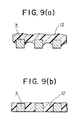
- the liquid adhesive of the present invention is to be applied onto a dam bar portion by the above-enumerated application stage, the liquid adhesive is also somewhat penetrated between lead pins to create a sectional shape as in Fig. 9 (a). Thereafter, via the above-mentioned pressing stage and the curing stage, the liquid adhesive is completely charged in-between lead pins as shown in Fig 9 (b), making it possible to act as the dam bar.
- the resin thickness at this time is approximately equal to the thickness of the leadframe, which means that there is no possibility of applying excessive pressure to the lead pins when molded.
- the curing of the liquid adhesive of the present invention proceeds to become a resin having a relatively high Young's modulus, thereby imparting the function as the dam bar.
- liquid adhesive of the present invention it is not necessary to remove the dam bar after transfer-molding, while retaining the portion of dam bar 2 during the production of the leadframe, as shown in Fig. 1, as is the conventional case, leading to saved labor and cost. Furthermore, the following problems in the case of using an insulating tape for electronic parts in which a polyimide film is used as a base film, and which has several results in terms of the lock of pins and insulating properties can be solved:
- a heat sink 10 having a semiconductor chip 6 provided thereon and lead pins 3 are adhered via an insulating adhesive layer 9, and the semiconductor chip and lead pins are connected via a bonding wire, and they are molded with a molding resin.
- the liquid adhesive of the present invention is applied in a prescribed pattern to either, or both, of the heat sink and lead pins by the dispensing method or the screen printing method, and then the heat sink and the leadframe are simply placed, after which the liquid adhesive is thermally cured. This makes it possible to cure the liquid adhesive while maintaining the insulating properties.
- the lead pins and the semiconductor chip are adhered with the liquid adhesive of the present invention, after a prescribed adhesive pattern is formed by the dispensing method or the screen printing method similar to the above embodiments, they can be adhered while maintaining the insulation between them. In this case, the problems caused by the use of the double-faced adhesive tape, such as by the application of pressure, temperature and impact upon the chip can be avoided.
- a resin pattern or an insulating layer can be formed by applying the liquid adhesive to various electronic parts by the dispensing method or the screen printing method, and curing the adhesive.
- a liquid adhesive was produced in the same manner as in Example 1, except that the amount of the acrylonitrile-butadiene copolymer having piperazinylethylaminocarbonyl groups at both terminals was changed from 50 parts by weight to 80 parts by weight, and the amount of the compound of the formula (II-1) was changed from 50 parts by weight to 20 parts by weight.
- a liquid adhesive was produced in the same manner as in Example 1, except that the amount of the acrylonitrile-butadiene copolymer having piperazinylethylaminocarbonyl groups at both terminals was changed from 50 parts by weight to 20 parts by weight, and the amount of the compound of the formula (II-1) was changed from 50 parts by weight to 80 parts by weight.
- a liquid adhesive was produced in the same manner as in Example 1, except that a compound represented by formula (I-2) having a weight average molecular weight of 50,000, an acrylonitrile content of 25% by weight, and an amino equivalent of 5,000 was used instead of the acrylonitrile-butadiene copolymer having piperazinylethylaminocarbonyl groups at both terminals, and the amount of toluene was changed from 200 parts to 400 parts.
- a compound represented by formula (I-2) having a weight average molecular weight of 50,000, an acrylonitrile content of 25% by weight, and an amino equivalent of 5,000 was used instead of the acrylonitrile-butadiene copolymer having piperazinylethylaminocarbonyl groups at both terminals, and the amount of toluene was changed from 200 parts to 400 parts.
- a liquid adhesive was produced in the same manner as in Example 1, except that a compound represented by formula (II-4) was used instead of the compound represented by formula (II-1).
- a liquid adhesive was produced in the same manner as in Example 1, except that a type of compound represented by formula (II-6) (2000 MP, produced by MITSUBISHI PETROCHEMICAL COMPANY, LRD.) was used instead of the compound represented by formula (II-1).
- a liquid adhesive was produced in the same manner as in Example 1, except that 2-ethyl-4-methylimidazole was used instead of benzoyl peroxide.
- a liquid adhesive was obtained by adding 1 part by weight of benzoyl peroxide to 100 parts by weight of epoxy acrylate (R-551, produced by NIPPON KAYAKU CO.LTD.).
- nylon-epoxy resin Teikoku Kagaku Sangyo K.K.
- a liquid adhesive was obtained by adding to 20 parts by weight of alumina (UA-5105, produced by SHOWA DENKO K.K.) to 500 parts by weight of a 20% strength solution of polyimide varnish (Lark TPI, produced by MITSUI TOATSU CHEMICALS INC.) in N-methylpyrrolidone, based on 100 parts by weight of the solid content of the above solution.
- the leadframe as shown in Fig. 1 was assembled according to the following procedures.
- a liquid adhesive was applied to the position shown in Fig. 1 (a) to form an adhesive pattern, and the adhesive was dried and cured under the conditions shown in Table 1.
- the produced leadframe was used to assemble a package according to the following procedures.
- the reason why the conditions of adhesion under pressing and the conditions of curing were different when assembling the package is that the characteristics of the adhesives are different from each other.
- optimum conditions for each adhesive were selected, and the adhesive was cured based on such conditions.
- a semiconductor chip was adhered to a plane portion with a silver paste for die bonding, which was then cured at 150 °C for 2 hours.
- a wire pad on the semiconductor chip and a silver plated portion at the end of the inner lead were connected with a gold wire.
- the packaging was finished.
- the wire bondability onto the leadframe at the wire bonding and the adhesive strength were confirmed. These are considered to be an index of heat resistance of the resin.
- Example 2 Good None 10-40 125/832 #2 Bad #3 Bad Comp.
- Example 3 Good Observed #1 2-4 0/83 Good Bad #1 Since the drying temperature was too high, the oxidation of the surface of the leadframe started. #2 The gold wire was wired but lacked sufficient strength. #3 The shorting was confirmed within 336 hours.
- the liquid adhesive obtained from Example 1 was used.
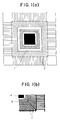
- a leadframe having no metallic dam bar as shown in Fig. 8 was used as a substrate, and a pattern was applied on the portion where the dam bar is originally placed.
- nitrogen heated at 150 °C was blown onto the pattern for 30 minutes to carry out drying.
- a presser having Teflon coated on the face with which the adhesive pattern is in contact was used to press the pattern at 150 °C for 30 minutes, thereby embedding the pattern into the gaps between lead pins, while molding the package into a shape where no unevenness was present on the upper surface of the pattern.
- the adhesive pattern was heated in an infrared-heating furnace whose interior had been replaced by a nitrogen atmosphere at 250 °C for 5 minutes to obtain an intended dam bar-equipped leadframe.
- a leadframe provided with a resin-made dam bar was obtained in the same manner as in Example 8, except that the liquid adhesive obtained from Example 2 was used, and the adhesive was applied by the screen printing.
- a leadframe provided with a resin-made dam bar was obtained in the same manner as in Example 8, except that the nylon-epoxy resin obtained from Comparative Example 2 was used, and the adhesive was thermally cured in an hot-air oven at 150°C for 3 hours.
- a conventional locking tape for a leadframe (produced by Tomoegawa Paper Co., LTD., ELEPHANE R-722) was used to tape a dam bar portion, and thermally cured in a hot air oven at 150 °C for 3 hours to obtain a leadframe equipped with a polyimide base film-provided dam bar.
Landscapes
- Chemical & Material Sciences (AREA)
- Organic Chemistry (AREA)
- Health & Medical Sciences (AREA)
- Chemical Kinetics & Catalysis (AREA)
- Medicinal Chemistry (AREA)
- Polymers & Plastics (AREA)
- Adhesives Or Adhesive Processes (AREA)
- Die Bonding (AREA)
- Lead Frames For Integrated Circuits (AREA)
Applications Claiming Priority (2)
| Application Number | Priority Date | Filing Date | Title |
|---|---|---|---|
| JP05292474A JP3137518B2 (ja) | 1993-10-29 | 1993-10-29 | 電子部品用液状接着剤およびそれを用いる絶縁接着層の形成方法 |
| JP292474/93 | 1993-10-29 |
Publications (2)
| Publication Number | Publication Date |
|---|---|
| EP0651040A1 true EP0651040A1 (fr) | 1995-05-03 |
| EP0651040B1 EP0651040B1 (fr) | 1997-12-29 |
Family
ID=17782285
Family Applications (1)
| Application Number | Title | Priority Date | Filing Date |
|---|---|---|---|
| EP94116992A Expired - Lifetime EP0651040B1 (fr) | 1993-10-29 | 1994-10-27 | Adhésif liquide pour composants électroniques et procédé pour formes une couche adhésive isolante en utilisant le même |
Country Status (5)
| Country | Link |
|---|---|
| US (1) | US5446080A (fr) |
| EP (1) | EP0651040B1 (fr) |
| JP (1) | JP3137518B2 (fr) |
| KR (1) | KR100287239B1 (fr) |
| DE (1) | DE69407538T2 (fr) |
Cited By (4)
| Publication number | Priority date | Publication date | Assignee | Title |
|---|---|---|---|---|
| EP0801424A3 (fr) * | 1996-04-10 | 1997-10-22 | Oki Electric Ind Co Ltd | |
| WO1998012746A1 (fr) * | 1996-09-21 | 1998-03-26 | Mci Computer Gmbh | Composant a semiconducteur et son procede de production |
| EP0902468A1 (fr) * | 1997-09-10 | 1999-03-17 | Oki Electric Industry Co., Ltd. | Dispositif semi-conducteur scellé par une résine et procédé de sa fabrication |
| WO2003044115A3 (fr) * | 2001-11-16 | 2003-11-20 | Lord Corp | Adhesifs permettant de lier des elastomeres durcis de peroxyde |
Families Citing this family (16)
| Publication number | Priority date | Publication date | Assignee | Title |
|---|---|---|---|---|
| JP2590747B2 (ja) * | 1994-07-29 | 1997-03-12 | 日本電気株式会社 | 半導体装置の製造方法 |
| JP2896751B2 (ja) * | 1995-03-30 | 1999-05-31 | 株式会社巴川製紙所 | 電子部品用接着テープ |
| JP2896754B2 (ja) * | 1995-06-08 | 1999-05-31 | 株式会社巴川製紙所 | 電子部品用接着テープ |
| JP3535281B2 (ja) * | 1995-08-31 | 2004-06-07 | 株式会社巴川製紙所 | 電子部品用接着テープ及び液状接着剤 |
| FR2741191B1 (fr) * | 1995-11-14 | 1998-01-09 | Sgs Thomson Microelectronics | Procede de fabrication d'un micromodule, notamment pour cartes a puces |
| US5904500A (en) * | 1996-10-03 | 1999-05-18 | The Dexter Corporation | Method for the preparation of lead-on-chip assemblies |
| US5840598A (en) * | 1997-08-14 | 1998-11-24 | Micron Technology, Inc. | LOC semiconductor assembled with room temperature adhesive |
| KR100481527B1 (ko) * | 1998-04-02 | 2005-06-08 | 삼성전자주식회사 | 다이 본딩 장치 |
| JP2000210800A (ja) | 1999-01-27 | 2000-08-02 | Komatsu Ltd | 産業機械のモニタ方法およびその装置 |
| EP1180918B1 (fr) * | 2000-08-16 | 2010-01-27 | Ericsson AB | Procédé pour dispenser de l'adhésif sur un membre de support d'un panneau à circuit et panneau à circuit ainsi obtenu |
| US6751099B2 (en) * | 2001-12-20 | 2004-06-15 | Intel Corporation | Coated heat spreaders |
| DE112004002845T5 (de) * | 2004-05-13 | 2007-03-08 | The Yokohama Rubber Co., Ltd. | Kautschuk mit endständigem Maleinimid und härtbare Zusammensetzungen, hergestellt unter Verwendung des Kautschuks mit endständigem Maleinimid |
| JP4995764B2 (ja) * | 2008-04-25 | 2012-08-08 | 力成科技股▲分▼有限公司 | リード支持型半導体パッケージ |
| JP6022761B2 (ja) | 2011-12-02 | 2016-11-09 | スリーエム イノベイティブ プロパティズ カンパニー | 両面接着材の製造方法 |
| KR101366394B1 (ko) * | 2012-04-09 | 2014-02-25 | 앰코 테크놀로지 코리아 주식회사 | 반도체 디바이스 및 그 제조 방법 |
| CN103943598B (zh) * | 2014-03-31 | 2016-08-17 | 山东华芯半导体有限公司 | 一种通用预封装基板结构、封装结构及封装方法 |
Citations (2)
| Publication number | Priority date | Publication date | Assignee | Title |
|---|---|---|---|---|
| FR2314207A1 (fr) * | 1975-06-13 | 1977-01-07 | Goodrich Co B F | Polymeres liquides a terminaison amine et leur procede d'obtention |
| JPH03275785A (ja) * | 1990-03-26 | 1991-12-06 | Hitachi Chem Co Ltd | 接着剤組成物及び半導体装置の製造法 |
Family Cites Families (4)
| Publication number | Priority date | Publication date | Assignee | Title |
|---|---|---|---|---|
| US2958672A (en) * | 1956-11-19 | 1960-11-01 | Du Pont | Curing process for high molecular weight polymers involving the use of free radical generators and free radical acceptors and product thereof |
| US5087681A (en) * | 1982-12-24 | 1992-02-11 | Secretary Of State For Defence In Her Majesty's Government Of United Kingdom | Composition from reacting vinylidene terminated polybutadiene/acrylonitrile and bisimide |
| US4918260A (en) * | 1985-07-26 | 1990-04-17 | Preleg, Inc. | Adhesive-coated wire and method and printed circuit board using same |
| US5364700A (en) * | 1985-12-27 | 1994-11-15 | Amoco Corporation | Prepregable resin composition and composite |
-
1993
- 1993-10-29 JP JP05292474A patent/JP3137518B2/ja not_active Expired - Fee Related
-
1994
- 1994-10-27 DE DE69407538T patent/DE69407538T2/de not_active Expired - Fee Related
- 1994-10-27 US US08/329,816 patent/US5446080A/en not_active Expired - Lifetime
- 1994-10-27 EP EP94116992A patent/EP0651040B1/fr not_active Expired - Lifetime
- 1994-10-28 KR KR1019940027991A patent/KR100287239B1/ko not_active Expired - Fee Related
Patent Citations (2)
| Publication number | Priority date | Publication date | Assignee | Title |
|---|---|---|---|---|
| FR2314207A1 (fr) * | 1975-06-13 | 1977-01-07 | Goodrich Co B F | Polymeres liquides a terminaison amine et leur procede d'obtention |
| JPH03275785A (ja) * | 1990-03-26 | 1991-12-06 | Hitachi Chem Co Ltd | 接着剤組成物及び半導体装置の製造法 |
Non-Patent Citations (1)
| Title |
|---|
| DATABASE WPI Week 9204, Derwent World Patents Index; AN 92-028979 * |
Cited By (8)
| Publication number | Priority date | Publication date | Assignee | Title |
|---|---|---|---|---|
| EP0801424A3 (fr) * | 1996-04-10 | 1997-10-22 | Oki Electric Ind Co Ltd | |
| US6097083A (en) * | 1996-04-10 | 2000-08-01 | Oki Electric Industry Co., Ltd. | Semiconductor device which is crack resistant |
| KR100366110B1 (ko) * | 1996-04-10 | 2003-02-19 | 오끼 덴끼 고오교 가부시끼가이샤 | 반도체장치및그실장방법 |
| WO1998012746A1 (fr) * | 1996-09-21 | 1998-03-26 | Mci Computer Gmbh | Composant a semiconducteur et son procede de production |
| EP0902468A1 (fr) * | 1997-09-10 | 1999-03-17 | Oki Electric Industry Co., Ltd. | Dispositif semi-conducteur scellé par une résine et procédé de sa fabrication |
| US6274938B1 (en) | 1997-09-10 | 2001-08-14 | Oki Electric Industry Co., Ltd. | Resin-sealed semiconductor device and method of manufacturing the device |
| US6541306B2 (en) | 1997-09-10 | 2003-04-01 | Oki Electric Industry Co., Ltd. | Resin-sealed semiconductor device and method of manufacturing the device |
| WO2003044115A3 (fr) * | 2001-11-16 | 2003-11-20 | Lord Corp | Adhesifs permettant de lier des elastomeres durcis de peroxyde |
Also Published As
| Publication number | Publication date |
|---|---|
| JP3137518B2 (ja) | 2001-02-26 |
| KR950011577A (ko) | 1995-05-15 |
| DE69407538T2 (de) | 1998-05-07 |
| EP0651040B1 (fr) | 1997-12-29 |
| KR100287239B1 (ko) | 2001-04-16 |
| DE69407538D1 (de) | 1998-02-05 |
| US5446080A (en) | 1995-08-29 |
| JPH07130772A (ja) | 1995-05-19 |
Similar Documents
| Publication | Publication Date | Title |
|---|---|---|
| EP0651040B1 (fr) | Adhésif liquide pour composants électroniques et procédé pour formes une couche adhésive isolante en utilisant le même | |
| EP0649892B1 (fr) | Ruban adhésif pour composants électroniques et adhésif liquide | |
| EP1701361B1 (fr) | Adhesif conducteur à faible contrainte | |
| EP0649893B1 (fr) | Ruban adhésif pour composants électroniques et adhésif liquide | |
| EP1597332B1 (fr) | Compositions adhesives conductrices stables electriquement et presentant une bonne resistance au choc, a utiliser dans des dispositifs electroniques | |
| EP0747399B1 (fr) | Ruban adhésif pour composants électroniques et adhésif liquide | |
| US5863988A (en) | Liquid adhesive for electronic parts and adhesive tape | |
| JP2896751B2 (ja) | 電子部品用接着テープ | |
| KR101401162B1 (ko) | 전자 부품용 액상 접착제 및 접착 테이프 | |
| JP2006176549A (ja) | エポキシ樹脂組成物及び半導体装置 | |
| JP2896755B2 (ja) | 電子部品用接着テープ | |
| JP3118420B2 (ja) | 電子部品用液状接着剤および接着テープ | |
| JP3118404B2 (ja) | 電子部品用液状接着剤および接着テープ | |
| JPH09241601A (ja) | 電子部品用液状接着剤およびそれを用いる絶縁接着層の形成方法 | |
| JP2896752B2 (ja) | 電子部品用接着テープ | |
| JP2002129116A (ja) | 半導体装置用接着テープ | |
| JP2001019821A (ja) | ダイアタッチペースト及びそれを用いた半導体装置 | |
| JP4404576B2 (ja) | 電子部品用接着テープ | |
| JP2001019722A (ja) | ダイアタッチペースト及びそれを用いた半導体装置 | |
| JP2003277486A (ja) | 片面封止用エポキシ樹脂組成物及び片面封止型半導体装置 | |
| JP2004352961A (ja) | 電子部品用接着テープ | |
| JPH10316956A (ja) | 硬化ニジミのない電子材料用エポキシ系接着剤 | |
| JPH06207082A (ja) | 半導体封止用樹脂組成物及び半導体装置 |
Legal Events
| Date | Code | Title | Description |
|---|---|---|---|
| PUAI | Public reference made under article 153(3) epc to a published international application that has entered the european phase |
Free format text: ORIGINAL CODE: 0009012 |
|
| AK | Designated contracting states |
Kind code of ref document: A1 Designated state(s): DE FR GB |
|
| 17P | Request for examination filed |
Effective date: 19950602 |
|
| GRAG | Despatch of communication of intention to grant |
Free format text: ORIGINAL CODE: EPIDOS AGRA |
|
| 17Q | First examination report despatched |
Effective date: 19970121 |
|
| GRAH | Despatch of communication of intention to grant a patent |
Free format text: ORIGINAL CODE: EPIDOS IGRA |
|
| GRAH | Despatch of communication of intention to grant a patent |
Free format text: ORIGINAL CODE: EPIDOS IGRA |
|
| GRAA | (expected) grant |
Free format text: ORIGINAL CODE: 0009210 |
|
| AK | Designated contracting states |
Kind code of ref document: B1 Designated state(s): DE FR GB |
|
| REF | Corresponds to: |
Ref document number: 69407538 Country of ref document: DE Date of ref document: 19980205 |
|
| ET | Fr: translation filed | ||
| PLBE | No opposition filed within time limit |
Free format text: ORIGINAL CODE: 0009261 |
|
| STAA | Information on the status of an ep patent application or granted ep patent |
Free format text: STATUS: NO OPPOSITION FILED WITHIN TIME LIMIT |
|
| 26N | No opposition filed | ||
| PGFP | Annual fee paid to national office [announced via postgrant information from national office to epo] |
Ref country code: FR Payment date: 20010928 Year of fee payment: 8 |
|
| PGFP | Annual fee paid to national office [announced via postgrant information from national office to epo] |
Ref country code: DE Payment date: 20011011 Year of fee payment: 8 |
|
| PGFP | Annual fee paid to national office [announced via postgrant information from national office to epo] |
Ref country code: GB Payment date: 20011031 Year of fee payment: 8 |
|
| REG | Reference to a national code |
Ref country code: GB Ref legal event code: IF02 |
|
| PG25 | Lapsed in a contracting state [announced via postgrant information from national office to epo] |
Ref country code: GB Free format text: LAPSE BECAUSE OF NON-PAYMENT OF DUE FEES Effective date: 20021027 |
|
| PG25 | Lapsed in a contracting state [announced via postgrant information from national office to epo] |
Ref country code: DE Free format text: LAPSE BECAUSE OF NON-PAYMENT OF DUE FEES Effective date: 20030501 |
|
| GBPC | Gb: european patent ceased through non-payment of renewal fee | ||
| PG25 | Lapsed in a contracting state [announced via postgrant information from national office to epo] |
Ref country code: FR Free format text: LAPSE BECAUSE OF NON-PAYMENT OF DUE FEES Effective date: 20030630 |
|
| REG | Reference to a national code |
Ref country code: FR Ref legal event code: ST |