EP0902468A1 - Dispositif semi-conducteur scellé par une résine et procédé de sa fabrication - Google Patents
Dispositif semi-conducteur scellé par une résine et procédé de sa fabrication Download PDFInfo
- Publication number
- EP0902468A1 EP0902468A1 EP19980115366 EP98115366A EP0902468A1 EP 0902468 A1 EP0902468 A1 EP 0902468A1 EP 19980115366 EP19980115366 EP 19980115366 EP 98115366 A EP98115366 A EP 98115366A EP 0902468 A1 EP0902468 A1 EP 0902468A1
- Authority
- EP
- European Patent Office
- Prior art keywords
- resin layer
- semiconductor chip
- leads
- lead
- filler
- Prior art date
- Legal status (The legal status is an assumption and is not a legal conclusion. Google has not performed a legal analysis and makes no representation as to the accuracy of the status listed.)
- Granted
Links
Images


Classifications
-
- H—ELECTRICITY
- H10—SEMICONDUCTOR DEVICES; ELECTRIC SOLID-STATE DEVICES NOT OTHERWISE PROVIDED FOR
- H10W—GENERIC PACKAGES, INTERCONNECTIONS, CONNECTORS OR OTHER CONSTRUCTIONAL DETAILS OF DEVICES COVERED BY CLASS H10
- H10W70/00—Package substrates; Interposers; Redistribution layers [RDL]
- H10W70/40—Leadframes
- H10W70/411—Chip-supporting parts, e.g. die pads
- H10W70/415—Leadframe inner leads serving as die pads
-
- H—ELECTRICITY
- H10—SEMICONDUCTOR DEVICES; ELECTRIC SOLID-STATE DEVICES NOT OTHERWISE PROVIDED FOR
- H10W—GENERIC PACKAGES, INTERCONNECTIONS, CONNECTORS OR OTHER CONSTRUCTIONAL DETAILS OF DEVICES COVERED BY CLASS H10
- H10W72/00—Interconnections or connectors in packages
- H10W72/071—Connecting or disconnecting
- H10W72/073—Connecting or disconnecting of die-attach connectors
- H10W72/07351—Connecting or disconnecting of die-attach connectors characterised by changes in properties of the die-attach connectors during connecting
- H10W72/07352—Connecting or disconnecting of die-attach connectors characterised by changes in properties of the die-attach connectors during connecting changes in structures or sizes
-
- H—ELECTRICITY
- H10—SEMICONDUCTOR DEVICES; ELECTRIC SOLID-STATE DEVICES NOT OTHERWISE PROVIDED FOR
- H10W—GENERIC PACKAGES, INTERCONNECTIONS, CONNECTORS OR OTHER CONSTRUCTIONAL DETAILS OF DEVICES COVERED BY CLASS H10
- H10W72/00—Interconnections or connectors in packages
- H10W72/071—Connecting or disconnecting
- H10W72/075—Connecting or disconnecting of bond wires
-
- H—ELECTRICITY
- H10—SEMICONDUCTOR DEVICES; ELECTRIC SOLID-STATE DEVICES NOT OTHERWISE PROVIDED FOR
- H10W—GENERIC PACKAGES, INTERCONNECTIONS, CONNECTORS OR OTHER CONSTRUCTIONAL DETAILS OF DEVICES COVERED BY CLASS H10
- H10W72/00—Interconnections or connectors in packages
- H10W72/30—Die-attach connectors
- H10W72/321—Structures or relative sizes of die-attach connectors
-
- H—ELECTRICITY
- H10—SEMICONDUCTOR DEVICES; ELECTRIC SOLID-STATE DEVICES NOT OTHERWISE PROVIDED FOR
- H10W—GENERIC PACKAGES, INTERCONNECTIONS, CONNECTORS OR OTHER CONSTRUCTIONAL DETAILS OF DEVICES COVERED BY CLASS H10
- H10W72/00—Interconnections or connectors in packages
- H10W72/50—Bond wires
- H10W72/531—Shapes of wire connectors
- H10W72/536—Shapes of wire connectors the connected ends being ball-shaped
-
- H—ELECTRICITY
- H10—SEMICONDUCTOR DEVICES; ELECTRIC SOLID-STATE DEVICES NOT OTHERWISE PROVIDED FOR
- H10W—GENERIC PACKAGES, INTERCONNECTIONS, CONNECTORS OR OTHER CONSTRUCTIONAL DETAILS OF DEVICES COVERED BY CLASS H10
- H10W72/00—Interconnections or connectors in packages
- H10W72/50—Bond wires
- H10W72/531—Shapes of wire connectors
- H10W72/5363—Shapes of wire connectors the connected ends being wedge-shaped
-
- H—ELECTRICITY
- H10—SEMICONDUCTOR DEVICES; ELECTRIC SOLID-STATE DEVICES NOT OTHERWISE PROVIDED FOR
- H10W—GENERIC PACKAGES, INTERCONNECTIONS, CONNECTORS OR OTHER CONSTRUCTIONAL DETAILS OF DEVICES COVERED BY CLASS H10
- H10W72/00—Interconnections or connectors in packages
- H10W72/50—Bond wires
- H10W72/551—Materials of bond wires
- H10W72/552—Materials of bond wires comprising metals or metalloids, e.g. silver
- H10W72/5522—Materials of bond wires comprising metals or metalloids, e.g. silver comprising gold [Au]
-
- H—ELECTRICITY
- H10—SEMICONDUCTOR DEVICES; ELECTRIC SOLID-STATE DEVICES NOT OTHERWISE PROVIDED FOR
- H10W—GENERIC PACKAGES, INTERCONNECTIONS, CONNECTORS OR OTHER CONSTRUCTIONAL DETAILS OF DEVICES COVERED BY CLASS H10
- H10W72/00—Interconnections or connectors in packages
- H10W72/851—Dispositions of multiple connectors or interconnections
- H10W72/853—On the same surface
- H10W72/865—Die-attach connectors and bond wires
-
- H—ELECTRICITY
- H10—SEMICONDUCTOR DEVICES; ELECTRIC SOLID-STATE DEVICES NOT OTHERWISE PROVIDED FOR
- H10W—GENERIC PACKAGES, INTERCONNECTIONS, CONNECTORS OR OTHER CONSTRUCTIONAL DETAILS OF DEVICES COVERED BY CLASS H10
- H10W74/00—Encapsulations, e.g. protective coatings
-
- H—ELECTRICITY
- H10—SEMICONDUCTOR DEVICES; ELECTRIC SOLID-STATE DEVICES NOT OTHERWISE PROVIDED FOR
- H10W—GENERIC PACKAGES, INTERCONNECTIONS, CONNECTORS OR OTHER CONSTRUCTIONAL DETAILS OF DEVICES COVERED BY CLASS H10
- H10W90/00—Package configurations
- H10W90/701—Package configurations characterised by the relative positions of pads or connectors relative to package parts
- H10W90/731—Package configurations characterised by the relative positions of pads or connectors relative to package parts of die-attach connectors
- H10W90/736—Package configurations characterised by the relative positions of pads or connectors relative to package parts of die-attach connectors between a chip and a stacked lead frame, conducting package substrate or heat sink
-
- H—ELECTRICITY
- H10—SEMICONDUCTOR DEVICES; ELECTRIC SOLID-STATE DEVICES NOT OTHERWISE PROVIDED FOR
- H10W—GENERIC PACKAGES, INTERCONNECTIONS, CONNECTORS OR OTHER CONSTRUCTIONAL DETAILS OF DEVICES COVERED BY CLASS H10
- H10W90/00—Package configurations
- H10W90/701—Package configurations characterised by the relative positions of pads or connectors relative to package parts
- H10W90/751—Package configurations characterised by the relative positions of pads or connectors relative to package parts of bond wires
- H10W90/756—Package configurations characterised by the relative positions of pads or connectors relative to package parts of bond wires between a chip and a stacked lead frame, conducting package substrate or heat sink
Definitions
- the present invention relates to a resin-sealed semiconductor device such as an IC or an LSI and a method of manufacturing the same.
- a resin-sealed semiconductor device comprises a semiconductor chip and a lead connected to the electrode of the semiconductor chip.
- the distal end of the lead and the semiconductor chip are sealed by a resin.
- the whole size of the resin-sealed semiconductor device including the sealing resin is determined by the standards. And generally, the size of the semiconductor chip increases as the degree of integration of the circuit increases.
- an LOC (Lead On Chip) type structure in which the distal end of the lead overlaps a semiconductor chip is generally employed.
- Japanese Patent Application Laid-Open No. 61-218139 discloses an LOC type resin-sealed semiconductor device.
- the distal end of a lead 1 is adhered to a semiconductor chip 3 through an insulating tape 4, and the distal end and an electrode 1b of the semiconductor chip 3 are connected to each other with a bonding wire 5.
- the semiconductor chip 3, the distal end of the lead 1, and the bonded portions are covered with the sealing resin layer 2.
- the sealing resin layer 2 generally consists of an epoxy-based resin whose ratio by weight is about 20% and filler whose ratio by weight is about 80%.
- the filler is silica-based solid bodies each having a diameter of 50 to 100 ⁇ m and has a function of keeping the hardness of a resin layer and a function of suppressing thermal expansion.
- the present invention aims to solve the problems of the prior art described above, and its object is to provide a resin-sealed semiconductor device which employs an LOC type structure, suppresses formation of cracks in a sealing resin layer by heat in practical use, and can prevent flaws or cracks from being formed in a semiconductor chip in solidification of the sealing resin layer.
- a resin-sealed semiconductor device comprises: a semiconductor chip having a circuit surface on which a plurality of electrodes are formed; a plurality of leads which are arranged at predetermined gaps with respect to the semiconductor chip in such a manner that distal ends of the leads overlap the semiconductor chip, and which electrically connected to the respective electrodes; a lead fixing resin layer filled between the semiconductor chip and the leads to fix the leads to the semiconductor chip; and a sealing resin layer which is coated to cover the distal ends of the leads and the semiconductor chip, and when the lead fixing resin layer contains filler, the diameter of the filler is smaller than the diameter of filler contained in the sealing resin layer, or the lead fixing resin layer is free from filler.
- the diameter of the filler is preferably about 1/10 to 1/5 the diameter of the filler contained in the sealing resin layer, or the diameter is preferably about 1/10 an gap between the leads and the semiconductor chip at an overlapping portion therebetween, i.e., the diameter is preferably about 10 ⁇ m.
- a ratio by weight of the filler contained in the lead fixing resin layer is preferably lower than a ratio by weight of the filler contained in the sealing resin layer.
- a method of manufacturing a resin-sealed semiconductor device which is constituted by sealing a semiconductor chip and leads with a sealing resin layer, comprises: the step of coating a lead fixing resin layer on a circuit surface of the semiconductor chip; the step of fixing the distal ends of a plurality of leads to the semiconductor chip with the lead fixing resin layer; the step of bonding the distal ends of the leads and electrodes formed on the circuit surface; and the step of sealing the semiconductor chip and the leads with the sealing resin layer.
- the lead fixing resin layer contains filler having a diameter smaller than that of filler contained in the sealing resin layer, or is free from filler.
- a resin-sealed semiconductor device is an LOC type semiconductor device comprising a semiconductor chip 3, a lead 1, a lead fixing resin layer 9 and a sealing resin layer 2.
- the semiconductor chip 3 is provided with a circuit surface 3a (serving as an upper surface in FIG. 1), and an electrode 10 is formed on the circuit surface 3a.
- the lead 1 is arranged at a predetermined gap with respect to the semiconductor chip 3 in such a manner that the distal end of the lead 1 overlaps the semiconductor chip 3.
- a bonding wire 5 electrically connects the distal end of the lead 1 and the electrode 10.
- the lead fixing resin layer 9 is filled between the semiconductor chip 3 and the lead 1 to fix the lead 1 to the semiconductor chip 3.
- the electrode 10 is formed on the semiconductor chip 3 such that a plurality of electrodes 10 are arranged in two lines at the central portion of the circuit surface 3a as shown in FIG. 2(A) serving as the side view and FIG. 2(B) serving as the plane view.
- the lead 1 connected to the electrodes 10 is formed such that a plurality of leads 1 are arranged in correspondence with the number of electrodes.
- the gap between the circuit surface 3a of the semiconductor chip 3 and the distal end of the lead 1 is about 40 to 100 ⁇ m.
- the lead fixing resin layer 9 is filled between the lead 1 and the circuit surface 3a over a range from the distal end of the lead 1 to the periphery of the semiconductor chip 3, i.e., a range in which the lead 1 overlaps the semiconductor chip 3.
- the sealing resin layer 2 contains filler having a diameter of 50 to 100 ⁇ m at a ratio by weight of about 80%, and the remaining 20% is an epoxy-based resin.
- the lead fixing resin layer 9 also consists of filler and an epoxy-based resin.
- the diameter of the filler is about 1/10 to 1/5 the diameter of the filler contained in the sealing resin layer 2, and is about 1/10 the gap between the lead 1 and the semiconductor chip 3 at the overlapping portion therebetween.
- the ratio by weight of the filler contained in the lead fixing resin layer 9 is set to be lower than the ratio by weight of the filler contained in the sealing resin layer 2. More specifically, the lead fixing resin layer 9 contains filler which has a diameter of about 10 ⁇ m and whose ratio by weight is about 40%, and the remaining 60% consists of an epoxy-based resin.
- the lead fixing resin layer 9 contains filler
- a material being free from filler can also be used as the lead fixing resin layer 9.
- This manufacturing method comprises: the first step of coating the lead fixing resin layer 9 on the circuit surface 3a of the semiconductor chip 3; the second step of fixing the distal ends of the plurality of leads 1 to the semiconductor chip 3 with the lead fixing resin layer 9; the third step of bonding the distal ends of the leads 1 and the electrodes 10 formed on the circuit surface 3a to each other; and the fourth step of sealing the semiconductor chip 3 and the leads 1 with the sealing resin layer 2.
- the respective steps will be sequentially described below.
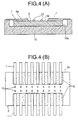
- a resin 9a for forming the lead fixing resin layer 9 is liquefied, and the liquid resin 9a is supplied from a dispenser 11 onto the circuit surface 3a.
- the resin 9a is coated on a position where the leads 1 are fixed, i.e., both the sides of electrode rows in the arrangement direction of the electrodes 10.
- the coated liquid resin 9a initially formes hemisphere shape in the first step.
- the semiconductor chip 3 is set in a recessed portion 12a formed in a heat block 12, and the plurality of leads 1 are pressed against the liquid resin 9a from the upper side of FIG. 4(A) to spread the liquid resin 9a.
- the heat block 12 is kept at a temperature of 80°C to 100°C, and the lead fixing resin layer 9 serving as a thermosetting resin is solidified for about one minute.
- the depth of the recessed portion 12a is set such that the level of the circuit surface 3a is lower than a periphery surrounding surface of the recessed portion 12a by 40 to 100 ⁇ m.
- the lead 1 is arranged to extend from both the sides of the semiconductor chip 3 to the central electrode 10 as shown in FIG. 4(B) serving as a plan view, and the lead 1 is fixed to the semiconductor chip 3 with the lead fixing resin layer 9.
- the electrode 10 of the semiconductor chip 3 is electrically connected to the distal end of the lead 1 fixed to the semiconductor chip 3 in the second step by bonding with the wire 5.
- the semiconductor chip 3, the distal end of the lead 1, and the wire 5 are sealed with the sealing resin layer 2, and the sealing resin layer 2 is solidified. Thereafter, lead processes such as diver cutting, lead cutting, and lead bending are performed to complete the semiconductor device shown in FIG. 1.
- a lead fixing resin layer when used to fix a lead before bonding to a semiconductor chip, a moisture content in the fixed portion decreases. For this reason, steam generated by heat in practical use can be suppressed, and probability of forming cracks in the sealing resin layer can be reduced.
- the diameter of filler contained in the lead fixing resin layer is reduced, probability of clogging the filler between the lead and the semiconductor chip can be reduced.
- the diameter of filler itself is reduced, the filler can be prevented from being clogged, and the semiconductor can be prevented from being cracked in solidification of the sealing resin.
- the filler content in the lead fixing resin layer is made smaller than that in the sealing resin layer, probability of clogging filler between the lead and the circuit surface can be reduced.
- filler clogging can be canceled. In this manner, stress based on the difference between the coefficient of contraction of the resin and the coefficient of contraction of the filler in solidification of the sealing resin can be prevented from being generated, so that the semiconductor chip can be prevented from being cracked.
Landscapes
- Structures Or Materials For Encapsulating Or Coating Semiconductor Devices Or Solid State Devices (AREA)
- Encapsulation Of And Coatings For Semiconductor Or Solid State Devices (AREA)
Applications Claiming Priority (3)
| Application Number | Priority Date | Filing Date | Title |
|---|---|---|---|
| JP24580897 | 1997-09-10 | ||
| JP24580897A JPH1187572A (ja) | 1997-09-10 | 1997-09-10 | 樹脂封止半導体装置およびその製造方法 |
| JP245808/97 | 1997-09-10 |
Publications (2)
| Publication Number | Publication Date |
|---|---|
| EP0902468A1 true EP0902468A1 (fr) | 1999-03-17 |
| EP0902468B1 EP0902468B1 (fr) | 2004-10-27 |
Family
ID=17139159
Family Applications (1)
| Application Number | Title | Priority Date | Filing Date |
|---|---|---|---|
| EP19980115366 Expired - Lifetime EP0902468B1 (fr) | 1997-09-10 | 1998-08-14 | Dispositif semi-conducteur scellé par une résine et procédé de sa fabrication |
Country Status (7)
| Country | Link |
|---|---|
| US (2) | US6274938B1 (fr) |
| EP (1) | EP0902468B1 (fr) |
| JP (1) | JPH1187572A (fr) |
| KR (1) | KR100382965B1 (fr) |
| CN (1) | CN100342528C (fr) |
| DE (1) | DE69827212T2 (fr) |
| TW (1) | TW392316B (fr) |
Families Citing this family (5)
| Publication number | Priority date | Publication date | Assignee | Title |
|---|---|---|---|---|
| US6577018B1 (en) * | 2000-08-25 | 2003-06-10 | Micron Technology, Inc. | Integrated circuit device having reduced bow and method for making same |
| SG102637A1 (en) * | 2001-09-10 | 2004-03-26 | Micron Technology Inc | Bow control in an electronic package |
| US7053967B2 (en) * | 2002-05-23 | 2006-05-30 | Planar Systems, Inc. | Light sensitive display |
| CN100378937C (zh) * | 2002-05-31 | 2008-04-02 | 威宇科技测试封装有限公司 | 利用焊线技术在芯片上布线的方法 |
| JP2011023458A (ja) * | 2009-07-14 | 2011-02-03 | Toshiba Corp | 半導体装置およびその製造方法 |
Citations (5)
| Publication number | Priority date | Publication date | Assignee | Title |
|---|---|---|---|---|
| US5068712A (en) * | 1988-09-20 | 1991-11-26 | Hitachi, Ltd. | Semiconductor device |
| US5286679A (en) * | 1993-03-18 | 1994-02-15 | Micron Technology, Inc. | Method for attaching a semiconductor die to a leadframe using a patterned adhesive layer |
| US5300459A (en) * | 1989-12-28 | 1994-04-05 | Sanken Electric Co., Ltd. | Method for reducing thermal stress in an encapsulated integrated circuit package |
| EP0651040A1 (fr) * | 1993-10-29 | 1995-05-03 | Tomoegawa Paper Co. Ltd. | Adhésif liquide pour composants électroniques et procédé pour formes une couche adhésive isolante en utilisant le même |
| WO1997029514A1 (fr) * | 1996-02-09 | 1997-08-14 | Mci Computer Gmbh | Composant a semi-conducteur |
Family Cites Families (7)
| Publication number | Priority date | Publication date | Assignee | Title |
|---|---|---|---|---|
| US5583375A (en) | 1990-06-11 | 1996-12-10 | Hitachi, Ltd. | Semiconductor device with lead structure within the planar area of the device |
| KR100234824B1 (ko) * | 1991-03-20 | 1999-12-15 | 윌리엄 비. 켐플러 | 반도체 장치 |
| JP2934357B2 (ja) | 1992-10-20 | 1999-08-16 | 富士通株式会社 | 半導体装置 |
| JP2997379B2 (ja) * | 1993-03-26 | 2000-01-11 | 京セラ株式会社 | 半導体装置 |
| TW270213B (fr) * | 1993-12-08 | 1996-02-11 | Matsushita Electric Industrial Co Ltd | |
| JP3350269B2 (ja) * | 1995-02-09 | 2002-11-25 | 京セラ株式会社 | 半導体装置 |
| US5759875A (en) * | 1996-10-04 | 1998-06-02 | Micron Technology, Inc. | Reduced filler particle size encapsulant for reduction in die surface damage in LOC packages and method of use |
-
1997
- 1997-09-10 JP JP24580897A patent/JPH1187572A/ja active Pending
-
1998
- 1998-08-04 TW TW87112800A patent/TW392316B/zh not_active IP Right Cessation
- 1998-08-14 DE DE1998627212 patent/DE69827212T2/de not_active Expired - Fee Related
- 1998-08-14 EP EP19980115366 patent/EP0902468B1/fr not_active Expired - Lifetime
- 1998-09-04 KR KR10-1998-0036499A patent/KR100382965B1/ko not_active Expired - Fee Related
- 1998-09-09 US US09/150,044 patent/US6274938B1/en not_active Expired - Fee Related
- 1998-09-09 CN CNB981191258A patent/CN100342528C/zh not_active Expired - Fee Related
-
2001
- 2001-06-07 US US09/875,258 patent/US6541306B2/en not_active Expired - Fee Related
Patent Citations (5)
| Publication number | Priority date | Publication date | Assignee | Title |
|---|---|---|---|---|
| US5068712A (en) * | 1988-09-20 | 1991-11-26 | Hitachi, Ltd. | Semiconductor device |
| US5300459A (en) * | 1989-12-28 | 1994-04-05 | Sanken Electric Co., Ltd. | Method for reducing thermal stress in an encapsulated integrated circuit package |
| US5286679A (en) * | 1993-03-18 | 1994-02-15 | Micron Technology, Inc. | Method for attaching a semiconductor die to a leadframe using a patterned adhesive layer |
| EP0651040A1 (fr) * | 1993-10-29 | 1995-05-03 | Tomoegawa Paper Co. Ltd. | Adhésif liquide pour composants électroniques et procédé pour formes une couche adhésive isolante en utilisant le même |
| WO1997029514A1 (fr) * | 1996-02-09 | 1997-08-14 | Mci Computer Gmbh | Composant a semi-conducteur |
Non-Patent Citations (1)
| Title |
|---|
| AMAGAI M ET AL: "DEVELOPMENT OF A TAPELESS LEAD-ON-CHIP (LOC) PACKAGE", PROCEEDINGS OF THE ELECTRONIC COMPONENTS AND TECHNOLOGY CONFERENCE, WASHINGTON, MAY 1 - 4, 1994, no. CONF. 44, 1 May 1994 (1994-05-01), INSTITUTE OF ELECTRICAL AND ELECTRONICS ENGINEERS, pages 506 - 512, XP000479177 * |
Also Published As
| Publication number | Publication date |
|---|---|
| DE69827212T2 (de) | 2005-03-10 |
| US6541306B2 (en) | 2003-04-01 |
| CN100342528C (zh) | 2007-10-10 |
| EP0902468B1 (fr) | 2004-10-27 |
| CN1211074A (zh) | 1999-03-17 |
| KR19990029543A (ko) | 1999-04-26 |
| US6274938B1 (en) | 2001-08-14 |
| TW392316B (en) | 2000-06-01 |
| JPH1187572A (ja) | 1999-03-30 |
| US20020000676A1 (en) | 2002-01-03 |
| KR100382965B1 (ko) | 2003-08-21 |
| DE69827212D1 (de) | 2004-12-02 |
Similar Documents
| Publication | Publication Date | Title |
|---|---|---|
| JP3233535B2 (ja) | 半導体装置及びその製造方法 | |
| JP2000269166A (ja) | 集積回路チップの製造方法及び半導体装置 | |
| US20010038150A1 (en) | Semiconductor device manufactured by package group molding and dicing method | |
| EP0902468A1 (fr) | Dispositif semi-conducteur scellé par une résine et procédé de sa fabrication | |
| US6525411B1 (en) | Semiconductor package and method of fabricating the same | |
| US6265768B1 (en) | Chip scale package | |
| US7023027B2 (en) | Diode package having an anode and a cathode formed on one surface of a diode chip | |
| JPS5810841A (ja) | 樹脂封止形半導体装置 | |
| US6900080B2 (en) | Microelectronic package with reduced underfill and methods for forming such packages | |
| US20030082852A1 (en) | Flip chip package and method for forming the same | |
| JP4361828B2 (ja) | 樹脂封止型半導体装置 | |
| US5043793A (en) | Semiconductor device with stress relief coating at the periphery of the device | |
| JPS59117250A (ja) | 半導体装置 | |
| JP3354716B2 (ja) | 半導体集積回路装置の製造方法 | |
| JP2570457B2 (ja) | 半導体装置 | |
| US20050006741A1 (en) | Substrate-based chip package | |
| JPH0511661B2 (fr) | ||
| KR100333383B1 (ko) | 반도체 패키지의 솔더 볼 접합 강도 강화 방법 | |
| JPH01135052A (ja) | 半導体装置およびその製造方法 | |
| JP2826432B2 (ja) | 半導体装置 | |
| JP2680969B2 (ja) | 半導体記憶装置 | |
| KR200202059Y1 (ko) | 브이·씨·에이패키지의칩본딩용접착제 | |
| JPH02285649A (ja) | 半導体装置 | |
| JPH03203338A (ja) | 半導体装置 | |
| JPH03116744A (ja) | 半導体装置 |
Legal Events
| Date | Code | Title | Description |
|---|---|---|---|
| PUAI | Public reference made under article 153(3) epc to a published international application that has entered the european phase |
Free format text: ORIGINAL CODE: 0009012 |
|
| AK | Designated contracting states |
Kind code of ref document: A1 Designated state(s): DE FR GB NL |
|
| AX | Request for extension of the european patent |
Free format text: AL;LT;LV;MK;RO;SI |
|
| 17P | Request for examination filed |
Effective date: 19990803 |
|
| AKX | Designation fees paid |
Free format text: DE FR GB NL |
|
| 17Q | First examination report despatched |
Effective date: 20030401 |
|
| GRAP | Despatch of communication of intention to grant a patent |
Free format text: ORIGINAL CODE: EPIDOSNIGR1 |
|
| GRAS | Grant fee paid |
Free format text: ORIGINAL CODE: EPIDOSNIGR3 |
|
| RIN1 | Information on inventor provided before grant (corrected) |
Inventor name: ANZAI, NORITAKA Inventor name: OHUCHI, SHINJI |
|
| GRAA | (expected) grant |
Free format text: ORIGINAL CODE: 0009210 |
|
| AK | Designated contracting states |
Kind code of ref document: B1 Designated state(s): DE FR GB NL |
|
| REG | Reference to a national code |
Ref country code: GB Ref legal event code: FG4D |
|
| REF | Corresponds to: |
Ref document number: 69827212 Country of ref document: DE Date of ref document: 20041202 Kind code of ref document: P |
|
| PGFP | Annual fee paid to national office [announced via postgrant information from national office to epo] |
Ref country code: GB Payment date: 20050802 Year of fee payment: 8 |
|
| PGFP | Annual fee paid to national office [announced via postgrant information from national office to epo] |
Ref country code: NL Payment date: 20050818 Year of fee payment: 8 |
|
| PGFP | Annual fee paid to national office [announced via postgrant information from national office to epo] |
Ref country code: FR Payment date: 20050819 Year of fee payment: 8 |
|
| PLBE | No opposition filed within time limit |
Free format text: ORIGINAL CODE: 0009261 |
|
| STAA | Information on the status of an ep patent application or granted ep patent |
Free format text: STATUS: NO OPPOSITION FILED WITHIN TIME LIMIT |
|
| ET | Fr: translation filed | ||
| 26N | No opposition filed |
Effective date: 20050728 |
|
| PGFP | Annual fee paid to national office [announced via postgrant information from national office to epo] |
Ref country code: DE Payment date: 20051026 Year of fee payment: 8 |
|
| PG25 | Lapsed in a contracting state [announced via postgrant information from national office to epo] |
Ref country code: NL Free format text: LAPSE BECAUSE OF NON-PAYMENT OF DUE FEES Effective date: 20070301 Ref country code: DE Free format text: LAPSE BECAUSE OF NON-PAYMENT OF DUE FEES Effective date: 20070301 |
|
| GBPC | Gb: european patent ceased through non-payment of renewal fee |
Effective date: 20060814 |
|
| NLV4 | Nl: lapsed or anulled due to non-payment of the annual fee |
Effective date: 20070301 |
|
| REG | Reference to a national code |
Ref country code: FR Ref legal event code: ST Effective date: 20070430 |
|
| PG25 | Lapsed in a contracting state [announced via postgrant information from national office to epo] |
Ref country code: GB Free format text: LAPSE BECAUSE OF NON-PAYMENT OF DUE FEES Effective date: 20060814 |
|
| PG25 | Lapsed in a contracting state [announced via postgrant information from national office to epo] |
Ref country code: FR Free format text: LAPSE BECAUSE OF NON-PAYMENT OF DUE FEES Effective date: 20060831 |