EP0651266A2 - Verfahren und Anordnung für Substratspiegel mit beliebigen Winkeln zum Gebrauch in optischen Hybridsystemen - Google Patents
Verfahren und Anordnung für Substratspiegel mit beliebigen Winkeln zum Gebrauch in optischen Hybridsystemen Download PDFInfo
- Publication number
- EP0651266A2 EP0651266A2 EP94307652A EP94307652A EP0651266A2 EP 0651266 A2 EP0651266 A2 EP 0651266A2 EP 94307652 A EP94307652 A EP 94307652A EP 94307652 A EP94307652 A EP 94307652A EP 0651266 A2 EP0651266 A2 EP 0651266A2
- Authority
- EP
- European Patent Office
- Prior art keywords
- substrate
- angled
- light
- optical path
- reflective surface
- Prior art date
- Legal status (The legal status is an assumption and is not a legal conclusion. Google has not performed a legal analysis and makes no representation as to the accuracy of the status listed.)
- Withdrawn
Links
Images


Classifications
-
- G—PHYSICS
- G02—OPTICS
- G02B—OPTICAL ELEMENTS, SYSTEMS OR APPARATUS
- G02B6/00—Light guides; Structural details of arrangements comprising light guides and other optical elements, e.g. couplings
- G02B6/24—Coupling light guides
- G02B6/42—Coupling light guides with opto-electronic elements
- G02B6/4201—Packages, e.g. shape, construction, internal or external details
- G02B6/4204—Packages, e.g. shape, construction, internal or external details the coupling comprising intermediate optical elements, e.g. lenses, holograms
- G02B6/4214—Packages, e.g. shape, construction, internal or external details the coupling comprising intermediate optical elements, e.g. lenses, holograms the intermediate optical element having redirecting reflective means, e.g. mirrors, prisms for deflecting the radiation from horizontal to down- or upward direction toward a device
-
- G—PHYSICS
- G02—OPTICS
- G02B—OPTICAL ELEMENTS, SYSTEMS OR APPARATUS
- G02B6/00—Light guides; Structural details of arrangements comprising light guides and other optical elements, e.g. couplings
- G02B6/10—Light guides; Structural details of arrangements comprising light guides and other optical elements, e.g. couplings of the optical waveguide type
- G02B6/12—Light guides; Structural details of arrangements comprising light guides and other optical elements, e.g. couplings of the optical waveguide type of the integrated circuit kind
- G02B6/122—Basic optical elements, e.g. light-guiding paths
-
- G—PHYSICS
- G02—OPTICS
- G02B—OPTICAL ELEMENTS, SYSTEMS OR APPARATUS
- G02B6/00—Light guides; Structural details of arrangements comprising light guides and other optical elements, e.g. couplings
- G02B6/10—Light guides; Structural details of arrangements comprising light guides and other optical elements, e.g. couplings of the optical waveguide type
- G02B6/12—Light guides; Structural details of arrangements comprising light guides and other optical elements, e.g. couplings of the optical waveguide type of the integrated circuit kind
- G02B2006/12083—Constructional arrangements
- G02B2006/12104—Mirror; Reflectors or the like
Definitions
- This invention relates to hybrid electronic/optic systems and more particularly to the formation of angled surfaces in a substrate which alter the path of optical signals.
- Angled mirrored surfaces are of great utility in optic systems.
- surface emitting lasers SELs
- the 45° mirror is used to deflect light from its path in the plane of the laser cavity to an optical path normal to the plane for optical engagement with other devices.
- the 45° mirrors of the prior art are typically formed by an ion milling technique.
- a photoresist is applied to a substrate and exposed at the intended site for the mirror.
- the photoresist is applied so that other features present on the substrate will not be affected by subsequent processing steps.
- the photoresist is subsequently developed to create an opening at the site.
- the substrate is then fixed on a tilting table and held at the angle which is to be imparted to the surface which will form the mirror. In the case mentioned above, that angle is 45°.
- An ion beam of sufficient energy to erode the material is then focussed and directed at the surface such that a deep groove is formed in the substrate.
- the photoresist now hardened from previous processing steps, must be stripped off and the surface of the substrate cleaned.
- a wedge of material must be removed from the substrate.
- a second groove is formed in the substrate which will intersect with the first groove.
- photoresist must first be reapplied to protect the groove previously formed by the ion beam, exposed and developed to create a second opening at the surface of the substrate.
- the substrate is then positioned normal to the beam and the second groove is formed.
- the two grooves intersect such that a wedge of material is released from the substrate resulting in an angled surface on the substrate.
- the ion milling technique is complicated, requiring separate photolithographic steps for each exposure to the ion beam.
- a second technique for forming angled surfaces for various applications is known as crystallographic dependent etching.
- the difference in etch rates of the ⁇ 100> and ⁇ 111> crystalline planes of silicon is utilized to create an angled surface.
- a ⁇ 100> silicon substrate is coated with a silicon nitride or silicon dioxide film which is subsequently patterned using photolithographic methods and etching to form an etch mask for the bulk silicon. Edges of features in the silicon nitride mask are aligned with the ⁇ 111> planes intersecting the silicon surface.
- the exposed silicon ⁇ 100> surface is then subjected to wet chemical etches which erode ⁇ 100> orientation silicon at a greater rate than ⁇ 111> orientation silicon.
- the etch proceeds into the silicon bulk material, but the ⁇ 111> silicon planes intersecting the mask edges do not etch significantly. Since the ⁇ 100> and ⁇ 111> planes are oriented at 54.74° to each other, this results in a surface oriented 54.74° with respect to the silicon surface. The utility of this method is limited by the fact that the angle between the two surfaces is fixed at exactly 54.74°. Further, application of the silicon nitride or silicon dioxide film adds to the complexity of the overall process. In addition, any angular misalignment between the photoresist mask and the ⁇ 111> planes causes a translational misalignment in the position of the angular surface.
- a film of erodible material such as photoresist or photo-definable polyimide is applied to the surface of a substrate.
- the intended taper sites are then exposed to radiation which has an energy variation at the surface of the erodible material. This results in an angular taper in the material at the intended taper sites.
- the profile of the erodible material is transferred to the underlying substrate by use of an etcher, obtaining a tapered, reflective surface.
- two reflective surfaces having taper angles of less than 45° are formed in a substrate.
- One of the surfaces optically engages an incoming optical signal and deflects it to a modulator/switch. Depending upon the state of the modulator, either the optical signal is reflected to the second of the two surfaces or propagation of the signal ceases.
- two reflective surfaces are formed in a substrate where the surfaces are coated with an active semiconductor device.
- an optical signal engaging the first reflective surface will either be reflected to the second surface and then to other optical devices such as a detector, or propagation of the signal will cease.
- a modulator arranged in this manner allows for four passes of the optical signal through the active semiconductor region greatly enhancing the total modulation of the signal.
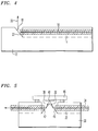
- an erodible material 2 is applied to the surface of a nonpolar substrate 1, such as silicon.
- a nonpolar substrate 1 such as silicon.
- Suitable erodible materials include, but are not limited to, photoresists and photo-definable polyimide.
- the erodible material 2 is characterized by a change in solubility upon exposure to appropriate radiation, typically ultraviolet light, although x-rays or electron beams may be used with certain materials. Exposure may increase or decrease solubility depending upon the nature of the erodible material.
- the erodible material 2 covering the intended taper region or regions 4 is then exposed to radiation.
- the radiation is applied so that it has an energy variation at the surface of the erodible material.
- the erodible material is then treated with a solvent that removes erodible material of higher solubility. This is referred to as "development.” After development, an angular taper 6 in the intended taper region 4 results as illustrated in FIG. 2.
- the films must first be removed at the intended taper sites by a method such as etching. Any means for etching through the films is acceptable. Examples include, but are not limited to, reactive ion etching, plasma ion etching, ion milling and wet chemical etching. After the films are removed, erodible material is applied.
- the linearly graded regions may be formed by a thin film of chromium or iron oxide of appropriately increasing or decreasing particle density.
- a thin film of inconel is used to create a photomask according to a process developed by Oxford Computer Inc., in Oxford, Connecticut. Film thickness is varied to achieve a linear variation in the energy incident upon the erodible material, resulting in the tapered profile 6 as shown in FIG. 2 and discussed above.
- a photomask comprising a slit of small width is positioned over the portion of the substrate coated with erodible material.
- the mask or substrate is held by a motorized micropositioner.
- the slit is scanned along the wafer, or vice versa, for the distance desired to form the exposed area.
- the rate at which the scanning occurs is varied to change the amount of energy incident upon any particular section of the desired area.
- the amount of erodible material remaining after exposure and subsequent development is directly dependent upon the amount of energy to which it was exposed.
- a taper or linear wedge 6 of erodible material will result as illustrated in FIG. 2.
- a fourth method for obtaining a tapered profile in the erodible material is known as E-beam lithography, which involves the use of a scanning electron beam.
- E-beam lithography involves the use of a scanning electron beam.
- a suitably programmed E-beam writer is scanned along the width of the intended growth region.
- a number of scanning passes are made across the width of the region, where, after each pass, the beam is indexed along the length of the intended growth region.
- each scan is performed at a slight lengthwise displacement from the previous scan. In this manner, the full area of the intended growth region is sequentially exposed.
- the energy of the beam is varied as required to alter the exposure depth to provide the desired taper.
- taper in the erodible material can be achieved by any of the aforementioned methods, other suitable means or methods for achieving such tapers may be used and are within the contemplated scope of this invention. It being recognized that other methods may readily occur to those skilled in the art in view of the teachings of the present invention.
- the wafer is then etched under conditions which etch both the erodible material and the substrate.
- the erodible layer remaining after development protects underlying layers from the etchant, i.e., the erodible layer is not etched.
- the erodible layer is etched as well as the substrate. This etching results in a tapered surface 8 on the substrate, as illustrated in FIG. 3.
- the erodible material acts as a sacrificial mask which provides a variable attenuation according to its taper in order to transfer the desired shape or angle into the underlying substrate. Reactive ion etching, plasma ion etching, ion milling, wet chemical etching or any other method or means suitable for etching both layers may be used.
- the relative etch rates of the erodible material and the bulk substrate can be altered.
- the relative etch rates can be changed by changing the oxygen content of the etchant gases.
- increasing the oxygen content increases the rate at which the substrate etches relative to the erodible material.
- a multiplicative effect is achieved, resulting in a greater angle in the substrate than in the erodible material.
- the tapered surface is suitably reflective.
- a coating or film of a reflective material may be applied to the tapered surface.
- Suitable reflective materials include, but are not limited to, metallic coatings or dielectric mirrors.
- a tapered reflective surface 22 optically engages optical signals 18 propagating along one or more waveguides 16 contained in a "vee" groove 14 in a substrate 12.
- the tapered reflective surface 22 is formed in the substrate 12 such that incoming optical signals 18 are deflected from a first optical path along waveguide 16 to a second optical path 20 upon optical engagement with surface 22.
- the second optical path 20, which is a function of the angle of tapered reflective surface 22, may then optically engage an optical component or a second reflective surface. In this manner, the optical signal may be directed to a different waveguide or various optical devices.
- the angle of the reflective surface is 45°. However, a reflective surface of any angle may be provided as required.
- the tapered reflective surface 22 may be formed as discussed above.
- first and second tapered reflective surface 40,42 are formed in a substrate 30, preferably as discussed above.
- Optical signals 36 propagating through one or more waveguides 34 located in vee groove 32, optically engage a first reflective surface 40.
- the optical signals 36 are directed to a modulation device 46 including an active semiconductor device 48.
- an active semiconductor device 48 Such a device has been reported by Boyd et al., "Multiple Quantum Well Reflection Modulator," APPL. PHYS. LETT. 50(17 at 1119-21 (1987).
- One suitable active semiconductor device for use as the active semiconductor device 48 is illustrated in FIG. 6.
- the device 48 is a multi-layer structure consisting of a periodic layer mirror 50, an electroabsorptive semiconductor 60, a transparent semiconductor contact 62 and, optionally, an anti-reflection coating 64.
- the periodic layer mirror consists of a number of periods 53,59, each of which is comprised of two layers 51, 52 or 57, 58 of transparent semiconductor material of differing refractive indices.
- the thickness of each layer typically one-quarter wavelength of the light in the layer, and number of periods are chosen to provide high reflectivity at a given operating wavelength via an optical interference effect.
- Two periods (four layers) are shown in FIG. 6 for clarity. However, a greater number of periods, typically twelve, are normally present.
- the mirror 50 is capped by an electroabsorptive semiconductor 60, i.e., a semiconductor in which light absorption at the operating wavelength is affected by an electric field.
- a transparent semiconductor contact 62 is formed on the electroabsorptive semiconductor 60.
- the mirror and contact layers are conductive so as to allow electrical bias to be applied to the electroabsorptive layer. Bias is delivered via electrodes 66 and 68 placed on these layers.
- the electroabsorptive layer is insulating so that a large electric field is produced across it upon application of bias.
- the absorptive capacity of the electroabsorptive material is a function of the applied bias, i.e., as bias is applied, light may be either absorbed or reflected dependant upon the design of the device.
- the reflectivity of the active semiconductor device is a function of the applied bias.
- the mirror and contact layers usually have differing electrical conductivity types, i.e., one is p-type and the other n-type, so as to form a diode.
- bias may be applied by reverse biasing the resulting diode which produces a field without current flow. This reduces the load of the device on the bias supply.
- the device may optionally include an anti-reflection coating 64, which is applied to the transparent semiconductor contact layer 62.
- Propagation of optical signals 38 to the second reflective surface 42 is thus dependent upon the state of the modulation device 46.
- the optical path from the first 40 to the second 42 reflective surface is enabled, allowing propagation of the signal.
- optical signals 36 will not propagate beyond the modulation device 46 since they are absorbed by the active semiconductor device 48.
- this arrangement may function as a switch.
- a light modulator may be formed using two angled reflective surfaces 72, 74 which are coated with an active semiconductor device 90.
- the angled surfaces 72 and 74 are formed in a substrate 70 such that the reflective surfaces face each other creating a vee-groove.
- the surfaces are preferably formed as taught by the present invention.
- An active semiconductor device 90 is formed on the angled surfaces 72 and 74.
- the structure of the active semiconductor device 90 is similar to that described above for device 48 of FIG. 6, consisting of a periodic layer mirror 80, an electroabsorptive semiconductor 82, a transparent semiconductor contact 84, electrodes 86 and 88, and an optional anti-reflection coating 89.
- the periodic layer mirror 80 is comprised of a number of layers of transparent semiconductor material 75, 76, 78, 79 as previously described. While four layers (two periods) are shown for clarity, additional layers are normally present.
- Optical signal 87 engages the active semiconductor device 90.
- the optical signal 87 makes four passes through electroabsorptive semiconductor 82, rather than two as in the second embodiment and in the prior art. The additional passes result in improved contrast.
- the angled surfaces result in a displacement of the reflected beam compared to the incident beam. This eliminates the need for the beamsplitters commonly employed in the prior art to achieve the same result, thus achieving a significant simplification of the optics. Compare Boyd et al., supra , at Fig. 1.
Landscapes
- Physics & Mathematics (AREA)
- General Physics & Mathematics (AREA)
- Optics & Photonics (AREA)
- Engineering & Computer Science (AREA)
- Microelectronics & Electronic Packaging (AREA)
- Mechanical Light Control Or Optical Switches (AREA)
- Optical Couplings Of Light Guides (AREA)
- Semiconductor Lasers (AREA)
- Optical Integrated Circuits (AREA)
Applications Claiming Priority (2)
| Application Number | Priority Date | Filing Date | Title |
|---|---|---|---|
| US146567 | 1980-05-05 | ||
| US14656793A | 1993-11-01 | 1993-11-01 |
Publications (2)
| Publication Number | Publication Date |
|---|---|
| EP0651266A2 true EP0651266A2 (de) | 1995-05-03 |
| EP0651266A3 EP0651266A3 (de) | 1997-12-10 |
Family
ID=22517986
Family Applications (1)
| Application Number | Title | Priority Date | Filing Date |
|---|---|---|---|
| EP94307652A Withdrawn EP0651266A3 (de) | 1993-11-01 | 1994-10-19 | Verfahren und Anordnung für Substratspiegel mit beliebigen Winkeln zum Gebrauch in optischen Hybridsystemen |
Country Status (4)
| Country | Link |
|---|---|
| US (1) | US5786925A (de) |
| EP (1) | EP0651266A3 (de) |
| JP (1) | JPH07176717A (de) |
| CA (1) | CA2130738A1 (de) |
Cited By (3)
| Publication number | Priority date | Publication date | Assignee | Title |
|---|---|---|---|---|
| EP1372005A3 (de) * | 2002-06-07 | 2004-11-17 | Fuji Photo Film Co., Ltd. | Integrierte optische Schaltung und Verfahren zu seiner Herstellung |
| WO2006102917A1 (en) * | 2005-03-31 | 2006-10-05 | Pirelli & C. S.P.A. | Method to fabricate a redirecting mirror in optical waveguide devices |
| US9052460B2 (en) | 2011-12-27 | 2015-06-09 | Neophotonics Corporation | Integrated circuit coupling system with waveguide circuitry and method of manufacture thereof |
Families Citing this family (41)
| Publication number | Priority date | Publication date | Assignee | Title |
|---|---|---|---|---|
| EP0804323B1 (de) * | 1995-01-18 | 1998-11-04 | Robert Bosch Gmbh | Anordnung zur umsetzung von optischen in elektrische signale und verfahren zur herstellung |
| TW365057B (en) * | 1997-12-31 | 1999-07-21 | Ind Tech Res Inst | Manufacturing method for micro-mirror on the silicon substrate |
| US6498870B1 (en) | 1998-04-20 | 2002-12-24 | Omm, Inc. | Micromachined optomechanical switches |
| DE19838519A1 (de) * | 1998-08-25 | 2000-03-02 | Bosch Gmbh Robert | Leiterplatte und Verfahren zur Herstellung |
| IT1308402B1 (it) * | 1999-03-03 | 2001-12-17 | Cselt Centro Studi Lab Telecom | Procedimento e dispositivo per accoppiare fibre ottiche e componentioptoelettronici. |
| TW460717B (en) * | 1999-03-30 | 2001-10-21 | Toppan Printing Co Ltd | Optical wiring layer, optoelectric wiring substrate mounted substrate, and methods for manufacturing the same |
| US6453083B1 (en) | 1999-05-28 | 2002-09-17 | Anis Husain | Micromachined optomechanical switching cell with parallel plate actuator and on-chip power monitoring |
| US6449406B1 (en) | 1999-05-28 | 2002-09-10 | Omm, Inc. | Micromachined optomechanical switching devices |
| US6445840B1 (en) | 1999-05-28 | 2002-09-03 | Omm, Inc. | Micromachined optical switching devices |
| US6445841B1 (en) | 1999-05-28 | 2002-09-03 | Omm, Inc. | Optomechanical matrix switches including collimator arrays |
| US6328484B1 (en) * | 2000-03-02 | 2001-12-11 | Agilent Technologies, Inc. | Fiber optic lens system for coupling fibers to surface mounted devices |
| US6434291B1 (en) | 2000-04-28 | 2002-08-13 | Confluent Photonics Corporations | MEMS-based optical bench |
| US6453087B2 (en) | 2000-04-28 | 2002-09-17 | Confluent Photonics Co. | Miniature monolithic optical add-drop multiplexer |
| US6496616B2 (en) | 2000-04-28 | 2002-12-17 | Confluent Photonics, Inc. | Miniature monolithic optical demultiplexer |
| US6810176B2 (en) | 2000-08-07 | 2004-10-26 | Rosemount Inc. | Integrated transparent substrate and diffractive optical element |
| US7003187B2 (en) | 2000-08-07 | 2006-02-21 | Rosemount Inc. | Optical switch with moveable holographic optical element |
| US6567574B1 (en) | 2000-10-06 | 2003-05-20 | Omm, Inc. | Modular three-dimensional optical switch |
| US6563997B1 (en) * | 2000-11-28 | 2003-05-13 | Lighteross, Inc. | Formation of a surface on an optical component |
| US20020158047A1 (en) * | 2001-04-27 | 2002-10-31 | Yiqiong Wang | Formation of an optical component having smooth sidewalls |
| US20020158046A1 (en) * | 2001-04-27 | 2002-10-31 | Chi Wu | Formation of an optical component |
| KR20030010035A (ko) * | 2001-07-25 | 2003-02-05 | 삼성전기주식회사 | 가변 광학 감쇠기 |
| JP2003240997A (ja) | 2002-02-21 | 2003-08-27 | Fujitsu Ltd | 空間反射型構造を有する光集積回路の製造方法 |
| US6775436B1 (en) | 2002-02-26 | 2004-08-10 | General Dynamics Advanced Technology Systems, Inc. | Optical fiber U-turn apparatus and method |
| CN1316271C (zh) * | 2002-03-01 | 2007-05-16 | 柔斯芒特公司 | 带有三维波导的光学开关 |
| US6885795B1 (en) | 2002-05-31 | 2005-04-26 | Kotusa, Inc. | Waveguide tap monitor |
| US6947622B2 (en) * | 2002-06-27 | 2005-09-20 | Kotura, Inc. | Wafer level testing of optical components |
| US7149376B2 (en) * | 2002-08-27 | 2006-12-12 | Ibiden Co., Ltd. | Embedded optical coupling in circuit boards |
| US6921490B1 (en) | 2002-09-06 | 2005-07-26 | Kotura, Inc. | Optical component having waveguides extending from a common region |
| US7308166B1 (en) | 2002-10-08 | 2007-12-11 | Kotura, Inc. | Coupling a light sensor array with an optical component |
| US7343058B2 (en) * | 2003-04-22 | 2008-03-11 | Intel Corporation | Efficient light coupler from off-chip to on-chip waveguides |
| JP2005062557A (ja) * | 2003-08-15 | 2005-03-10 | Canon Inc | 光素子装置、それを用いた二次元光導波路素子及び光電融合配線基板 |
| CN101176040A (zh) * | 2005-04-14 | 2008-05-07 | 哈佛大学 | 用于微制造的牺牲层中可调整的溶解度 |
| US7639912B2 (en) * | 2007-01-31 | 2009-12-29 | Hewlett-Packard Development Company, L.P. | Apparatus and method for subterranean distribution of optical signals |
| JP4962144B2 (ja) * | 2007-05-31 | 2012-06-27 | 日本電気株式会社 | 光モジュール |
| US7668420B2 (en) * | 2007-07-26 | 2010-02-23 | Hewlett-Packard Development Company, L.P. | Optical waveguide ring resonator with an intracavity active element |
| US8611707B2 (en) | 2009-01-09 | 2013-12-17 | Hewlett-Packard Development Company, L.P. | System and methods for routing optical signals |
| US9164231B2 (en) * | 2011-08-08 | 2015-10-20 | Oracle International Corporation | Ultra-compact photodetector on an optical waveguide |
| WO2013023245A1 (en) * | 2011-08-15 | 2013-02-21 | Globaltech Corporation Pty Ltd | Optical device for use with download equipment |
| EP3345030B1 (de) * | 2015-09-03 | 2019-07-24 | Telefonaktiebolaget LM Ericsson (publ) | System, verfahren und vorrichtung für optische rundsendungsübertragung in einer leiterplatte |
| US10234644B1 (en) * | 2017-10-20 | 2019-03-19 | Corning Optical Communications LLC | Optical-electrical printed circuit boards with integrated optical waveguide arrays and photonic assemblies using same |
| US20230025444A1 (en) * | 2021-07-22 | 2023-01-26 | Lawrence Livermore National Security, Llc | Systems and methods for silicon microstructures fabricated via greyscale drie with soi release |
Family Cites Families (17)
| Publication number | Priority date | Publication date | Assignee | Title |
|---|---|---|---|---|
| BE566967A (de) * | 1954-03-26 | |||
| US4136928A (en) * | 1977-05-06 | 1979-01-30 | Bell Telephone Laboratories, Incorporated | Optical integrated circuit including junction laser with oblique mirror |
| US4376160A (en) * | 1980-04-07 | 1983-03-08 | California Institute Of Technology | Method of making and structure for monolithic optical circuits |
| US4461535A (en) * | 1981-10-21 | 1984-07-24 | Bell Telephone Laboratories, Incorporated | Wavelength filters |
| JPS5925282A (ja) * | 1982-08-02 | 1984-02-09 | Fujitsu Ltd | 光伝送路付光半導体パツケ−ジ |
| US4564584A (en) * | 1983-12-30 | 1986-01-14 | Ibm Corporation | Photoresist lift-off process for fabricating semiconductor devices |
| US4751171A (en) * | 1984-07-03 | 1988-06-14 | Matsushita Electric Industrial Co., Ltd. | Pattern forming method |
| JPH0648546B2 (ja) * | 1984-07-14 | 1994-06-22 | 日本ビクター株式会社 | 情報記録担体の製造法 |
| US4732446A (en) * | 1985-10-02 | 1988-03-22 | Lamar Gipson | Electrical circuit and optical data buss |
| US4869780A (en) * | 1987-04-10 | 1989-09-26 | Trw Inc. | Ion milling method |
| JPS6450588A (en) * | 1987-08-21 | 1989-02-27 | Hikari Gijutsu Kenkyu Kaihatsu | Manufacture of optical path rise type semiconductor light-emitting element |
| JPH01282517A (ja) * | 1988-05-10 | 1989-11-14 | Furukawa Electric Co Ltd:The | 光変調器 |
| US5279924A (en) * | 1989-04-04 | 1994-01-18 | Sharp Kabushiki Kaisha | Manufacturing method of optical diffraction grating element with serrated gratings having uniformly etched grooves |
| US5170448A (en) * | 1992-01-06 | 1992-12-08 | Motorola, Inc. | Optical waveguide apparatus and method for partially collecting light |
| JPH05206025A (ja) * | 1992-01-27 | 1993-08-13 | Rohm Co Ltd | 微細加工方法 |
| US5310623A (en) * | 1992-11-27 | 1994-05-10 | Lockheed Missiles & Space Company, Inc. | Method for fabricating microlenses |
| EP0614101A3 (de) * | 1993-02-03 | 1994-10-19 | Canon Kk | Optischer Ablenker und Verfahren zu seiner Herstellung. |
-
1994
- 1994-08-23 CA CA002130738A patent/CA2130738A1/en not_active Abandoned
- 1994-10-19 EP EP94307652A patent/EP0651266A3/de not_active Withdrawn
- 1994-10-31 JP JP6288700A patent/JPH07176717A/ja active Pending
-
1996
- 1996-05-20 US US08/650,582 patent/US5786925A/en not_active Expired - Lifetime
Cited By (7)
| Publication number | Priority date | Publication date | Assignee | Title |
|---|---|---|---|---|
| EP1372005A3 (de) * | 2002-06-07 | 2004-11-17 | Fuji Photo Film Co., Ltd. | Integrierte optische Schaltung und Verfahren zu seiner Herstellung |
| US7197201B2 (en) | 2002-06-07 | 2007-03-27 | Fujifilm Corporation | Optical wiring substrate fabrication process and optical wiring substrate device |
| WO2006102917A1 (en) * | 2005-03-31 | 2006-10-05 | Pirelli & C. S.P.A. | Method to fabricate a redirecting mirror in optical waveguide devices |
| US7871760B2 (en) | 2005-03-31 | 2011-01-18 | Pgt Photonics S.P.A. | Method to fabricate a redirecting mirror in optical waveguide devices |
| US8236481B2 (en) | 2005-03-31 | 2012-08-07 | Google Inc. | Method to fabricate a redirecting mirror in optical waveguide devices |
| US9052460B2 (en) | 2011-12-27 | 2015-06-09 | Neophotonics Corporation | Integrated circuit coupling system with waveguide circuitry and method of manufacture thereof |
| US9329346B2 (en) | 2011-12-27 | 2016-05-03 | Neophotonics Corporation | Integrated circuit coupling system with waveguide circuitry and method of manufacture thereof |
Also Published As
| Publication number | Publication date |
|---|---|
| US5786925A (en) | 1998-07-28 |
| JPH07176717A (ja) | 1995-07-14 |
| EP0651266A3 (de) | 1997-12-10 |
| CA2130738A1 (en) | 1995-05-02 |
Similar Documents
| Publication | Publication Date | Title |
|---|---|---|
| US5786925A (en) | Method and composition for arbitrary angle mirrors in substrates for use in hybrid optical systems | |
| EP1866688B1 (de) | Verfahren zur herstellung eines umlenkspiegels in optischen wellenleiterbauelementen | |
| US5116461A (en) | Method for fabricating an angled diffraction grating | |
| US6351329B1 (en) | Optical attenuator | |
| US6913871B2 (en) | Fabricating sub-resolution structures in planar lightwave devices | |
| US6993225B2 (en) | Tapered structure for providing coupling between external optical device and planar optical waveguide and method of forming the same | |
| EP0110184B1 (de) | Herstellungsverfahren für integrierte Optik | |
| US20060098311A1 (en) | Micro-mirror and a method for fabricating the same | |
| US5894538A (en) | Method of forming integrated optical circuit planar waveguide turning mirrors | |
| EP0379358B1 (de) | Verfahren zur Herstellung eines Beugungsgitters für optische Elemente | |
| Strzelecka et al. | Fabrication of refractive microlenses in semiconductors by mask shape transfer in reactive ion etching | |
| US6170297B1 (en) | Jig for manufacturing long period grating filter and apparatus and method for manufacturing long period grating filter using the same | |
| WO1997040558A1 (en) | Vertical cavity lasers with monolithically integrated refractive microlenses | |
| US5443685A (en) | Composition and method for off-axis growth sites on nonpolar substrates | |
| Suhara et al. | Focusing grating coupler in AlGaAs optical waveguide | |
| JPS62296102A (ja) | 導波路グレ−テイング結合器 | |
| Matz et al. | Laser-induced dry etching of integrated InP microlenses. | |
| Dix et al. | Electron‐beam fabrication and focused ion beam inspection of submicron structured diffractive optical elements | |
| Swanton et al. | Use of e-beam written, reactive ion etched, phase masks for the generation of novel photorefractive fibre gratings | |
| EP0490320B1 (de) | Verfahren zur Herstellung eines Beugungsgitters | |
| US20050048409A1 (en) | Method of making an optical device in silicon | |
| Naumaan et al. | A geodesic optical waveguide lens fabricated by anisotropic etching | |
| JP2000180645A (ja) | 光導波路素子の光接続端面の形成方法 | |
| WO2004088715A2 (en) | Tapered structure for providing coupling between external optical device and planar optical waveguide and method of forming the same | |
| US6954002B2 (en) | System and method of enhancing alignment marks |
Legal Events
| Date | Code | Title | Description |
|---|---|---|---|
| PUAI | Public reference made under article 153(3) epc to a published international application that has entered the european phase |
Free format text: ORIGINAL CODE: 0009012 |
|
| AK | Designated contracting states |
Kind code of ref document: A2 Designated state(s): DE FR GB IT |
|
| PUAL | Search report despatched |
Free format text: ORIGINAL CODE: 0009013 |
|
| AK | Designated contracting states |
Kind code of ref document: A3 Designated state(s): DE FR GB IT |
|
| STAA | Information on the status of an ep patent application or granted ep patent |
Free format text: STATUS: THE APPLICATION IS DEEMED TO BE WITHDRAWN |
|
| 18D | Application deemed to be withdrawn |
Effective date: 19980612 |